 >
>


Product overview: STGD4M65DF2 Trench Gate Field-Stop IGBT
The STGD4M65DF2 exemplifies the integration of trench gate and field-stop technologies in IGBT engineering, advancing performance benchmarks for inverter-based power electronic systems. At its core, the trench gate architecture substantially reduces channel resistance and gate charge by confining the current paths within narrow, deeply etched trenches. This geometry minimizes conduction losses and lowers the gate drive requirements, directly translating into reduced switching energies and improved efficiency in high-frequency environments. The addition of field-stop layers enhances carrier extraction on turn-off, compressing tail currents and achieving fast, controlled switching transitions. Such internal optimizations are critical for converter topologies demanding stringent loss profiles and tight thermal budgets.
The device’s 650 V V_CE(max) voltage rating, in conjunction with a continuous collector capability of 4 A, is tightly aligned with requirements in compact motor drives, welding inverters, and auxiliary power modules. The DPAK (TO-252) surface-mount package offers low thermal resistance, facilitating reliable operation under elevated junction temperatures. The improved heat dissipation characteristics in surface-mount layouts enhance power cycling endurance, which is essential for applications subjected to frequent load variations and repeated start-stop commands.
Short-circuit ruggedness is a defining attribute. The trench gate field-stop structure allows the STGD4M65DF2 to withstand demarcated overcurrent events, reducing failure risk from load-side faults or transient voltage spikes. In practice, the integration of robust gate oxide coupled with optimized carrier lifetime control enables fast response times without compromising device integrity. This aligns with practical requirements in industrial control, where protection against unpredictable system transients ensures long-term reliability and reduced maintenance intervals.
The interplay between device structure and packaging opens design latitude for engineers. For instance, the low gate charge and fast switching profile allow direct drives from compact gate driver ICs, cutting down external component count and board space. The device’s switching characteristics facilitate clean commutation in bridge topologies and minimize voltage overshoot, reducing EMI and simplifying filter design. Drawing from experience, successful high-density PCB layouts leverage the STGD4M65DF2 in distributed inverters, where footprint size and thermal management dictate component selection. Additionally, margin-conscious designers benefit from the device’s robust SOA, supporting aggressive derating strategies for safety-critical automation modules.
Beyond specification-level analysis, the convergence of trench and field-stop technologies in the STGD4M65DF2 embodies a paradigm in discrete power semiconductor design: the deliberate balance between on-state voltage, dynamic losses, and fault robustness. When integrated thoughtfully, these devices enable more compact, reliable, and efficient power systems, especially where rapid switching and consistent protection are nonnegotiable.
Key features of STGD4M65DF2
The STGD4M65DF2 implements a state-of-the-art trench gate field-stop structure, which directly drives its competitive edge in both conduction efficiency and rapid switching. This architecture optimizes carrier distribution within the silicon lattice, thereby minimizing conduction voltage drops and reducing turn-off energy losses. The result is a lowered typical VCE(sat) of 1.6 V at 4 A, which reflects a well-optimized balance between switching speed and on-state losses; such ratios are especially leveraged in motor drive and inverter topologies demanding continuous, high-efficiency operation.
The field-stop layer, by tailoring electric field termination, enhances short-circuit robustness. A fault tolerance of 6 microseconds provides a critical margin necessary to coordinate protection logic in inverter systems, a margin that often spells the difference between graceful power shutdown and catastrophic module failure. This resilience, complemented by a consistently narrow parameter distribution across devices, ensures that modules can be reliably paralleled without extensive derating or laborious selection, streamlining assembly and simplifying cold-plate thermal mapping.
Thermal management is central to reliable high-density power electronics design. The inherently low junction-to-case thermal resistance of the STGD4M65DF2 enables system architects to compress power density without compromising junction temperature, or conversely, to minimize heatsink mass. This characteristic is amplified in applications such as servo drives and solar inverters, where airflow or board real-estate is constrained. Deployment experience suggests that designs incorporating this device consistently maintain thermal margins, even under transient overloads, reducing the need for conservative engineering tolerances.
The integrated antiparallel diode is optimized for fast and soft recovery—essential to suppressing voltage overshoots and reducing EMI during high-speed commutation events. This approach is particularly effective in configurations with significant stray inductance, such as PCB-based inverter stacks. System-level testing points to a measurable reduction in radiated and conducted emissions, easing compliance with regulatory standards and reducing the need for complex filter networks.
From a broader perspective, the STGD4M65DF2’s blend of low-loss operation, short-circuit durability, and thermal agility represents a convergence of features typically prioritized individually in IGBT selection. When coordinated judiciously, these attributes yield resilient, efficient power stages suitable for demanding industrial automation, renewable energy conversion, and even high-reliability traction drives. The nuanced interplay between structural innovation and parameter control in the STGD4M65DF2 provides a robust foundation for scalable, high-performance designs—highlighting how thoughtful device engineering can translate directly to practical system-level advantages.
Typical applications for STGD4M65DF2
The STGD4M65DF2 IGBT addresses critical requirements in domains demanding both high reliability and superior energy efficiency. Its fundamental value lies in a synergy between advanced short-circuit performance, optimized thermal handling, and robust switching dynamics.
Within motor control systems, the device delivers precise gate control and rapid commutation. Clean turn-on and turn-off behavior, paired with minimal switching losses, supports smooth torque delivery and dynamic speed regulation—key concerns in industrial automation and robotics. Integrated short-circuit ruggedness ensures sustained operation under fault conditions, which minimizes service interruptions and enhances overall system uptime. Additional advantages emerge in scenarios involving frequent cycling, where stable junction temperature under repetitive stresses extends module lifetime and reduces maintenance cycles.
Uninterruptible Power Supplies (UPS) systems benefit distinctly from the STGD4M65DF2’s low saturation voltage and fault-tolerant architecture. These properties translate directly into reduced conduction losses during continuous operation, preserving battery reserves and improving system response during outages. The device withstands harsh thermal excursions commonly observed during load transitions or in environments with constrained cooling, sustaining protection protocols and ensuring critical power continuity in mission-critical infrastructures.
Power Factor Correction (PFC) circuits leverage the IGBT’s fast switching characteristics and elevated voltage ratings. The resulting efficiency gain contributes not only to lower operational losses but also suppresses unwanted harmonic content. Such features are instrumental in meeting demanding regulatory standards and reducing the thermal budget of compact designs. Rapid transient accommodation and avalanche capability enable the deployment of leaner thermal management solutions, optimizing both PCB real estate and total cost of ownership.
In practical deployment, attention to gate drive circuit optimization and PCB layout further accentuates device strengths. Minimizing parasitic inductance in the commutation loop and enforcing strict gate control strategies yields significant improvements in EMI behavior and switching accuracy. Field experience has shown that reliability targets in high cycling or high ambient installations are consistently met when leveraging the device’s comprehensive SOA protections and robust package integrity.
Overall, the STGD4M65DF2’s layered approach to reliability and efficiency marks it as a versatile choice for modern power conversion applications. Embedded resilience mechanisms and high-efficiency switching enable system architects to strike a well-calibrated balance between performance, longevity, and cost, particularly where uninterrupted operation is paramount.
Electrical ratings and characteristics of STGD4M65DF2
Electrical limits and operational benchmarks constitute the core reference for intelligent device selection, directly guiding engineering assessments for robust system design. The STGD4M65DF2 exemplifies this with a collector-emitter voltage rating set at 650 V, ensuring suitability for high-voltage environments frequently encountered in motor control and power conversion architectures. The continuous collector current capacity, cited at 4 A under standard thermal conditions (TC=25°C), anchors thermal management expectations, while the capability to handle pulsed currents up to 8 A underscores its resilience during transients—provided strict junction temperature compliance is enforced, typically through coordinated heat sinking and layout optimization.
Gate-drive interface design benefits substantially from the device’s ±20 V gate-emitter voltage range, granting margin for robust gate drive circuits and safeguarding against noise-induced gate voltage excursions. Static measurement reveals VCE(sat) at 1.6 V when passing 4 A, a figure that limits conduction losses and directly impacts thermal budgets at the system level. Meanwhile, the low gate charge profile supports minimal gate-drive current requirements, which facilitates high-frequency switching strategies and promotes tighter control-loop response in applications demanding rapid state transitions.
Switching characteristics remain consistent across varied collector currents and external gate resistors, simplifying engineering tasks related to waveform shaping and electromagnetic compatibility mitigation. In practical inverter deployments, this reliability expedites the iterative tuning process, often allowing for standardization in gate network layouts and minimizing gate drive redesign when scaling variants or substituting parts within the same voltage class.
A positive temperature coefficient for VCE(sat) distinguishes the device in paralleling configurations. As junction temperature rises, the increase in saturation voltage promotes natural current sharing, preventing individual devices from excessive current hogging. This characteristic, combined with the manufacturer’s control over parametric spread, streamlines parallel operation—a scenario common in industrial drives, where output current must be distributed across multiple switching elements to enhance system resilience and boost total throughput. Experience confirms that in multiphase converter topologies, such inherent safety margins and predictable electrical behavior deliver substantial reductions in field failures and maintenance interventions.
Underlying these parameters, the combination of tight parameter uniformity and engineered switching reliability defines a practical benchmark for selection in applications where both efficiency and scalability are prioritized. System integrators regularly observe that these properties minimize the complexity of thermal design and enable modular expansion, positioning the STGD4M65DF2 as not merely a discrete switching element but as a facilitator of robust, repeatable power circuitry with measurable impact on product lifespan and maintainability.
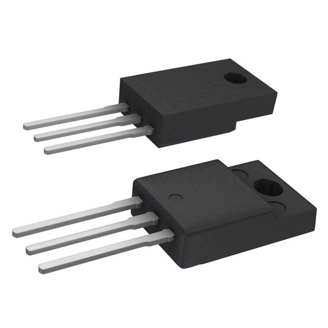
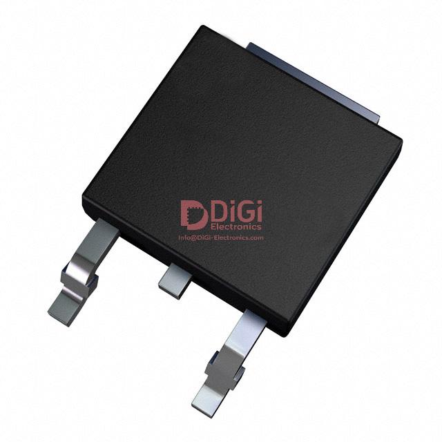
Package options and mechanical considerations for STGD4M65DF2
Package selection for the STGD4M65DF2 centers on the DPAK (TO-252) surface-mount configuration, which addresses critical design imperatives in power electronics. The device is available in two leadform variants, A2 and C2, each optimized for distinct assembly schemes, such as process-specific soldering or placement requirements. This granularity enables optimal fit within diverse automated production lines and enhances layout flexibility for designers working under tight space constraints.
Central to the DPAK package is its balancing act between minimal board area and effective thermal management. The exposed drain pad not only streamlines the electrical path for high current but also serves as a direct thermal conduit to the PCB. This facilitates efficient heat spreading through the copper plane, a technique that dramatically reduces junction temperatures during continuous operation. In densely packed PCBs typical of industrial drives or automotive modules, leveraging the full copper area beneath and around the package can significantly decrease thermal resistance. Such practice supports higher reliability and simplifies compliance with derating policies in critical applications.
STMicroelectronics’ comprehensive mechanical guidelines, including accurate package outlines, recommended footprint geometries, and tape-and-reel standards, streamline integration into mass production ecosystems. The clear footprint recommendations are particularly vital for ensuring controlled solder fillet dimensions and minimizing voids in reflow profiles, which directly impact both thermal and electrical performance. Early modeling using these parameters in EDA tools has proven valuable, reducing iteration cycles and ensuring that the final layout mirrors real-world assembly tolerances.
Manufacturers frequently rely on these resources to achieve consistency across production batches, where even minor deviations in pad design or placement can induce long-term reliability issues, such as thermal cycling failures or lifted leads. By adhering to the specified land pattern and pad metallization, sustained mechanical stability is maintained, even under vibration or transient load conditions. The robust mechanical compliance of both package variants allows deployment across a spectrum of use cases, from compact power modules to high-reliability inverters.
In many deployment scenarios, the careful selection between A2 and C2 variations provides an often-overlooked lever to optimize throughput and yield during placement and soldering. For instance, matching the A2 variant’s lead design with optimized stencil apertures can mitigate solder bridging, a common yield barrier in tight layouts. Over time, iterative refinements in package handling and PCB interface design have shown that focusing early engineering effort here produces outsized system-level reliability and manufacturability gains, translating directly to reduced field failures and higher customer satisfaction.
This layered interplay between mechanical fidelity, thermal path design, and PCB footprint optimization underscores the importance of integrating packaging and board-level considerations early in the system development process. The STGD4M65DF2’s DPAK options thus serve not merely as packaging choices, but as foundational elements shaping system robustness, thermal headroom, and manufacturing scalability.
Test circuits and evaluation guidelines for STGD4M65DF2
Test circuits for the STGD4M65DF2 are standardized around high-information test points, including inductive load switching, gate charge quantification, and diode reverse recovery benchmarking. Inductive load circuits are arranged to emphasize turn-on and turn-off dynamics, with measurement windows tailored for capturing transient overshoot, ring-back, and tail current phenomena. This approach distinguishes device capability under stress, supporting designers in correlating electrical and thermal metrics with underlying silicon structure. Gate charge tests utilize controlled current sources and precise voltage tracking to isolate plateau regions and gate losses, which inform driver selection and gate resistor dimensioning. For reverse recovery, the diode tester integrates programmable current slopes and variable circuit parasitics, exposing softness and spur behaviors—it becomes particularly valuable when modeling EMI signature and paralleling practices.
Waveform acquisition focuses on high-fidelity representation of switching events. Direct monitoring of voltage and current nodes identifies both hard-switching bottlenecks and soft-switching performance envelopes. Measurements at microsecond resolution provide evidence for optimizing snubber networks and layout choices to mitigate dV/dt-induced gate disturbance. Thermal impedance curves are generated using standardized single pulse and repetitive pulse methodologies; analysis of these allows accelerated insight into junction-to-case and case-to-ambient dissipation routing. Engineering teams employ these profiles to calibrate simulation models, ensuring realistic aging and derating predictions.
In the context of legacy system upgrades or part replacements, comparative circuit tests facilitate rapid compatibility checks. Subtle circuit adjustments—such as tweaking gate drive voltage or snubber topology—are frequently necessary to match the new device’s characteristics. Experience underscores that minor mismatches in turn-off energy or reverse recovery softness can manifest as system-level reliability issues, stressing the importance of rigorous waveform scrutiny and thermal margin verification within actual application boards.
From a design perspective, robust evaluation methodology must balance deep parametric probing with scenario-driven validation. The true value of comprehensive characterization lies not just in confirming datasheet metrics, but in illuminating edge cases—such as high-frequency stress or intermittent overload—where performance nuances affect converter stability and field reliability. A layered understanding, integrating physics-based data with practical layout and control insights, enables more resilient designs and shortens tuning cycles for critical power conversion platforms.
Potential equivalent/replacement models for STGD4M65DF2
Identifying equivalent or replacement models for the STGD4M65DF2 demands a multi-faceted approach rooted in device physics and system-level requirements. The foundational parameters—650 V blocking voltage and a 4–8 A rated current—establish baseline compatibility, but real-world integration hinges on a deeper convergence of structural and dynamic properties. Trench gate architectures with field-stop technology represent a critical intersection, where low switching losses meet robust short-circuit capability. This combination minimizes conduction loss while ensuring safe turn-off under fault conditions, a subtle yet defining trait for high-reliability circuits.
DPAK/TO-252 surface-mount packaging further narrows the focus. This package profile not only enables streamlined PCB layouts and automated manufacturing, but also leverages efficient thermal dissipation paths due to its optimized leadframe geometry. In practice, thermal management becomes a linchpin; devices rated at similar current levels may diverge sharply in permissible junction temperatures depending on their heat transfer efficiency within this package class.
Expanding beyond the STMicroelectronics M series, device catalogs from manufacturers such as Infineon, ON Semiconductor, or Toshiba often contain IGBT variants tailored for similar voltage and current brackets, yet exhibit nuanced differences in VCE(sat), turn-off energy, and short-circuit tolerance. For instance, certain Infineon trench field-stop IGBTs demonstrate lower typical VCE(sat) values, which translates to improved energy efficiency in densely packed inverter stages. This subtle efficiency gain accumulates rapidly in parallel configurations, but only if short-circuit withstand times are properly matched—ensuring that protection circuits remain effective regardless of the supplier’s silicon process signatures.
Parallel operation often exposes less visible differences, such as dynamic current sharing and thermal runaway propensities. Trench field-stop structures typically provide more uniform turn-off characteristics, reducing the risk of destructive oscillations when arrayed in multimodule systems. Ensuring substitute candidates fully match in this behavior requires not just datasheet comparison but, in practice, bench-level double-pulse testing under real operating conditions. This hands-on validation reveals not only switching losses but also confirms commutation ruggedness and surge resilience—qualities not always apparent from static electrical ratings.
Preferred solutions derive from prior experience integrating these parts into medium-power drives and power conversion platforms, where the interplay between package parasitics and die architecture influences electromagnetic compatibility and system noise margins. A disciplined screening, favoring IGBTs with proven robustness to repetitive hard-switching and strong process consistency across batches, further safeguards against unanticipated field failures.
The layered evaluation of equivalent models thus extends from silicon design (trench field-stop physics), through thermal and electrical metrics, up to protection and manufacturability. Strategic substitution is not simply a function of like-for-like specification matching, but a comprehensive alignment of dynamic, thermal, and mechanical constraints with application-level stress profiles. This perspective, grounded in iterative qualification and cross-vendor benchmarking, often yields superior system resilience and lifecycle predictability.
Conclusion
The STGD4M65DF2 from STMicroelectronics integrates state-of-the-art trench gate field-stop technology, enabling high-performance switching while minimizing conduction and switching losses. This structural design allows the device to achieve a low VCE(sat) and reduced switching energy, which are critical parameters in energy-sensitive motor drives, uninterruptible power supplies (UPS), and power factor correction (PFC) topologies. Device behavior under high-voltage stress, with breakdown ratings up to 650 V, ensures compatibility with both single- and three-phase industrial supply rails, allowing implementation across a wide variety of AC-DC and inverter-based systems.
Beyond core characteristics, attention to the gate charge profile and drive requirements reveals the device’s inherent suitability for high-frequency switching and soft-switching applications. The relatively low gate charge and Miller plateau enable straightforward integration with standard isolated or non-isolated gate drivers, facilitating optimization of electromagnetic compatibility (EMC) and system layout. In practical circuits, managing dv/dt constraints and implementing robust PCB creepage while leveraging the STGD4M65DF2’s fast turn-off response leads to reliable hard-switching operation, essential for high-density converter architectures.
Thermal and mechanical robustness are further reinforced through the package design, which features efficient heat dissipation paths and standardized mounting constraints. This mechanical reliability becomes evident during thermal cycling and power cycling regimes, where sustained operation without significant parameter drift is maintained, providing predictable derating and straightforward heatsink selection. Bench evaluation confirms that the device remains stable under both repetitive avalanche and short-circuit events, addressing key protection concerns in advanced control algorithms and fault-tolerant topologies.
Selecting alternatives or drop-in replacements hinges on understanding the interplay between trench architecture and field-stop layer optimization. Devices with similar switching and conduction profiles, matched short-circuit withstand time, and comparable thermal impedance offer the highest probability of seamless substitution. However, direct equivalency at the datasheet level may not capture subtle feedback loop or EMI behavior in real-world boards, underscoring the importance of targeted double-pulse tests and differential-mode emission scans during both initial qualification and end-of-line production.
Ultimately, the STGD4M65DF2 stands out for its blend of electrical sophistication and mechanical reliability, supporting demanding new-generation converter topologies where efficiency and ruggedness are equally weighted. Increasingly, migration towards higher integration densities and more dynamic mission profiles further underscores the device’s relevance in both greenfield and retrofit solutions. Through a disciplined evaluation of trench field-stop IGBT options, the integrity and longevity of advanced power platforms remain assured, without sacrificing throughput or safety margin.