 >
>


Product overview: STDRIVE601TR by STMicroelectronics
The STDRIVE601TR from STMicroelectronics delivers a highly integrated solution for three-phase power electronics. At its core, the device incorporates three discrete half-bridge gate drivers, each precisely engineered to handle both high-side and low-side switching tasks. The 600V rail support directly addresses the voltage domains prevalent in industrial motor drivers, solar inverters, and servo systems, where elevated isolation requirements and robust noise immunity are indispensable. By tightly coupling the gate drive capability to both MOSFETs and IGBTs, the STDRIVE601TR ensures optimal switching characteristics across varying load and topology scenarios.
The underlying architecture leverages level-shifting techniques to manage the stark potential differences between high-side and low-side gate signals. This distinction, managed through advanced bootstrap circuitry and shoot-through protection, enables safe and synchronized operation in three-phase bridge circuits. The driver’s pinout and pin protection features streamline PCB routing, minimizing gate trace inductance and reducing susceptibility to parasitic spikes and EMI, resulting in increased system reliability.
Integration of three matched half-bridges within a single package reduces the need for discrete gate drivers and auxiliary logic, simplifying engineering development cycles for multi-phase designs. Engineers accustomed to troubleshooting complex gate driver interactions find notable reductions in effort during board bring-up and validation, with observable improvements in thermal management and fault tolerance. Field experience substantiates that using the STDRIVE601TR leads to fewer instances of gate oscillation and cross-conduction in high-frequency inverter operation, an essential consideration for both hard- and soft-switching topologies.
Implementing the STDRIVE601TR in real-world motor control platforms accelerates design for systems such as variable-frequency drives, pump controllers, and industrial fans. Its ability to reliably handle rapid commutation and regenerative braking scenarios elevates operational efficiencies, especially in environments exposed to transient over-voltages. In PV inverter applications, predictable gate timing and robust undervoltage lockout safeguard power semiconductors during grid disturbances, reinforcing long-term system endurance.
From a system perspective, the triple half-bridge design provides an elegant foundation for modular multi-level converters and fractional horsepower motor controllers, reducing BOM size while simultaneously boosting overall circuit density. The device’s resilience to high dv/dt and its comprehensive support for standard logic interface voltages streamline successful integration across both legacy and emerging control platforms.
These layers of robustness and design efficiency reveal that deploying STDRIVE601TR enables compact, reliable, and cost-effective power conversion solutions, particularly when optimizing for high-performance industrial applications and future-proofing against evolving power semiconductor standards.
Key features of STDRIVE601TR
STDRIVE601TR integrates a comprehensive set of features optimized for robust high-voltage gate drive applications, particularly in demanding industrial settings. Its 600 V maximum voltage rail directly targets high-power conversion and motor drive topologies, supporting three-phase inverters, PFC stages, and other architectures where wide bus voltages and reliability are paramount. The device’s capability to source up to 200 mA and sink up to 350 mA (typical, 25°C) allows for rapid turn-on and turn-off of large MOSFETs or IGBTs. This ensures minimal switching losses and lower device temperature rise, critical for thermal management in dense power electronic assemblies.
A key underlying strength lies in the STDRIVE601TR’s transient immunity. With a ±50 V/ns dV/dt capability, the driver maintains logic integrity even in severe switching environments, significantly reducing susceptibility to noise spikes typical in hard-switched bridges or fast-PWM scenarios. This robustness is especially valuable in situations where long wire runs or parasitic elements elevate the risk of false triggering.
The gate drive supply flexibility—spanning 9 V to 20 V—enables compatibility with a wide range of discrete IGBTs or power MOSFETs, facilitating fine-tuning of gate charge currents for various device technologies. Input logic compatibility at both 3.3 V and 5 V TTL/CMOS levels streamlines signal interfacing with modern microcontrollers or FPGAs, reducing the need for level translation and minimizing design complexity.
Internal bootstrap diodes are a standout feature, directly supporting the high-side channel operation without requiring external fast recovery diodes. This not only shrinks PCB area but also enhances long-term reliability by eliminating a common point of field failure. Reliable operation across high and low sides is further reinforced by dedicated UVLO circuits, actively safeguarding against undervoltage conditions that could otherwise cause gate misfires and catastrophic half-bridge shoot-through.
The device’s protection concept is multi-layered. The comparator-driven fast overcurrent shutdown, linked with a smart shutdown path and programmable deadtime, provides real-time response to fault conditions and ensures that cross-conduction is physically prevented. Matching propagation delays—nominally 85 ns with tight skew across channels—ensure edge synchronicity in high-frequency PWM applications, preserving signal integrity during fast transitions and minimizing cycle distortion.
Interlock and deadtime programmability further contribute to system safety and efficiency. By allowing customization of deadtime intervals between phases, designers can achieve an optimal compromise between commutation loss reduction and cross-conduction immunity, essential in variable load or variable switching frequency contexts. The enable, FAULT, and OD pins offer instantaneous system response and detailed fault diagnostics via open-drain signalling—essential for both software-driven safety management and hardware-level fault intervention.
Practical experience highlights the pronounced reduction in external BOM—removing discrete bootstrap diodes and some current-limiting components—resulting in a leaner layout with lower parasitics and improved EMI behavior. The device’s strong noise immunity and accurate delay matching have proven crucial in field deployments involving long inverter output cables and high dv/dt transitions, where less robust drivers may succumb to spurious switching or increased shoot-through risk.
From an engineering perspective, the integration strategy behind STDRIVE601TR goes beyond mere feature accumulation; it orchestrates synergistic safety, efficiency, and compactness, making it an enabler for next-generation inverter and motor drive designs. This enables achieving higher power densities and reliability targets without increasing design complexity, supporting advancements in industrial automation and energy conversion systems. The approach exemplified by STDRIVE601TR underlines the convergence of smart protection and high-performance drivers as the linchpin for robust, future-ready power electronics architectures.
Electrical and thermal performance parameters of STDRIVE601TR
Electrical and thermal performance parameters of the STDRIVE601TR form the foundation for robust gate driver implementation in advanced power applications. The absolute maximum voltage rating of 600 V for the high-side rail enables direct deployment in environments where high bus voltages are present, particularly in industrial motor drives, power converters, and automotive inverters. This high-voltage tolerance is underpinned by reinforced isolation and gate drive architecture, safeguarding both switching components and system-level operation against transient spikes.
Driver output currents—200 mA for source and 350 mA for sink—are engineered for efficient and rapid gate-control cycles. These values optimize MOSFET and IGBT switching by swiftly charging and discharging gate capacitances, mitigating switching losses and minimizing dead-time distortion. The asymmetric source/sink balance is especially relevant in scenarios with large power switches, ensuring robust turn-off even when parasitic impedances are present. Practical deployment has shown that leveraging the higher sink capacity accelerates device turn-off, directly reducing shoot-through risk during phase commutations.
Input logic compatibility down to 3.3 V directly aligns with contemporary digital control architectures, supporting seamless integration with microcontrollers, DSPs, and FPGAs without level-shifting circuits. This allows for simplified board layouts and reduced design complexity, especially critical when scaling motor control systems or implementing wide input range power stages. The low input threshold also enhances noise immunity in electrically noisy environments, improving reliability in harsh industrial settings.
Precision is a core attribute, reflected in the propagation delay of 85 ns (typical) and tightly matched inter-channel delays. This enables high-frequency operation with synchronized switching, paving the way for accurate three-phase motor vector control and fine-grained modulation schemes. In practical multi-channel operation, the matched delays eliminate phase jitter, needed for applications demanding low harmonic distortion and precise torque response.
Moisture Sensitivity Level 3 classification for 168-hour exposure period informs storage and assembly protocols during surface mount processes. Correct handling as dictated by this rating prevents latent reliability defects, crucial for power modules required to operate over extended lifetimes in challenging environments. Data derived from extended exposure testing underscores the necessity of disciplined moisture management, especially for field-deployed systems subject to varied climates.
Thermal performance, specified under the JEDEC 2s2p PCB standard, provides critical data for thermal modeling and cooling system design. The standardized thermal resistance values enable predictive system-level analysis, facilitating informed decisions on heat sinking, airflow management, and PCB layout optimization. Operational feedback from deployed systems highlights the impact of effective thermal dissipation—poor management can accelerate device aging or trigger derating, while well-designed thermal paths preserve reliability across the full voltage and current spectrum.
The STDRIVE601TR's balance between electrical robustness, signal interfacing flexibility, switching precision, assembly reliability, and thermal transparency solidifies its position for high-speed, high-power application domains. A nuanced approach to device characteristics, supported by empirical deployment insights, reveals that optimal performance hinges not merely on specification adherence but on holistic integration into the circuit, thermal, and control architecture. Careful harmonization of these parameters ensures stable and efficient operation under both predictable and dynamic load scenarios.
Functional architecture and operation of STDRIVE601TR
The STDRIVE601TR is architected around three galvanically isolated, independent half-bridge gate drivers, directly addressing the requirements of three-phase power stages in inverter or motor control environments. Each channel features dedicated logic-level inputs for both high-side (HIN) and low-side (LIN) control, coordinated by a global Enable (EN) pin to facilitate synchronized or staged power-up and -down. This modular control allows the driver to support flexible PWM strategies and tailored switching schemes essential in advanced vector control or field-oriented control (FOC) systems.
At a hardware level, the device enforces matched propagation delays and output characteristics across all three channels. Such precise timing alignment is crucial for suppressing undesirable phase imbalance or circulating currents, especially at higher switching frequencies typical in modern inverter topologies. Programmable deadtime, injected automatically between half-bridge switching events, acts as a safeguard against cross-conduction and potential shoot-through, with the timing parameterized for varying IGBT or MOSFET technologies and load conditions. Interlocking logic supplements this by adding an additional layer of hardware-based protection, selectively preventing simultaneous conduction paths irrespective of logic input anomalies.
The input stage leverages CMOS/TTL-compatible logic, employing hysteresis to embolden immunity against high-frequency noise, an essential design consideration in electrically noisy motor-control environments. Integrated bootstrap diodes for each high-side respective channel streamline the board layout: their presence minimizes component count, yields reliable high-side supply biasing, and optimizes PCB routing for low parasitics. These factors directly translate to reduced EMI and higher power density in inverter power modules, as validated in prototype and mass-production drives.
Error handling is coordinated through an open-drain FAULT output, which, in conjunction with internal fast comparators, triggers immediate shut-down in response to critical events such as gate-driver undervoltage, overcurrent, or desaturation conditions. The fault response pathway operates independently from main logic control, facilitating rapid system-level intervention—this modular isolation accelerates diagnostic routines, as the FAULT state directly reflects real-time protection status without risk of software interpretation delays.
In field deployment, integrating the STDRIVE601TR significantly reduces design iterations centered on timing mismatch or fault isolation—its deterministic deadtime control and low-impedance error signaling alleviate common causes of inverter downtime. The compact, all-in-one driver architecture improves system-level MTBF by reducing wiring complexity and potential single-point failures often introduced by discrete gate-drive and fault-detection circuits. Furthermore, the device’s solid logic-level compatibility ensures streamlined digital interfacing with standard microcontrollers or DSPs, supporting both rapid prototyping and scalable production deployments.
Beyond technical attributes, a notable insight emerges: the convergence of robust protection, precise timing, and streamlined logic paths within a single gate driver forms an essential backbone for reliability and efficiency in scalable industrial and automotive power conversion solutions. Driving down PCB footprint while hardening fault response not only meets but redefines system constraints for new-generation motor control applications.
Protection, shutdown, and safety mechanisms in STDRIVE601TR
Robust safety and fault-tolerance are essential in precision motor drive and power conversion environments, where undetected faults can propagate swiftly and compromise system integrity. The STDRIVE601TR incorporates an array of protective mechanisms, each addressing distinct layers of potential risk through a tightly integrated architecture optimized for industrial reliability and application flexibility.
Underlying these protections is a voltage monitoring matrix consisting of both VCC and VBO undervoltage lockout (UVLO) circuits. The VCC UVLO persistently observes the primary gate driver supply rail, instantly suspending gate driver output when the supply drops below its critical threshold. This immediate isolation prevents gate misdrive events and avoids erratic switching behavior that could trigger destructive shoot-through current. Augmenting the global supply lockout, VBO UVLO independently protects each high-side bootstrap channel, recognizing that high-side gate driving is especially vulnerable to bootstrap undervoltage during dynamic operations. This per-channel vigilance ensures that no high-side device inadvertently conducts with insufficient gate charge—a common root cause of output stage failures in high-frequency drive scenarios.
The SmartSD function exemplifies responsive protection tailored for fast transient conditions. By employing a dedicated fast comparator circuit interfaced through the CIN pin, the system allows direct connection to external shunt resistors positioned for real-time current sensing at the output stage. Upon sensing overcurrent or overload excursions, the SmartSD circuitry commands an instantaneous shutdown, with propagation delay engineered to remain invariant regardless of external RC timing network selection. This deterministic response is crucial when deploying the system across diverse application profiles, from low-inductance BLDC drives to high-inertia industrial motors, where the reliability of shutdown timing materially influences equipment survivability.
Fault signaling and output-disable management provide higher-level oversight and customization. The FAULT pin enables synchronous notification to supervisory controllers or diagnostic modules whenever UVLO or SmartSD events occur, supporting seamless integration with broader system diagnostics or data logging frameworks. Output-disable timing, governed via the OD pin and programmable through external RC elements, facilitates nuanced recovery strategies—such as electro-mechanical debounce intervals or staged re-enablement—adapted to the load and system’s operational policy. This feature is particularly valuable in tightly regulated environments where transient faults must be isolated, logged, and only cautiously cleared, without risking premature reactivation.
In practice, these layered mechanisms translate to a platform that shortens circuit design cycles by reducing external safety hardware and points of failure. System builders can confidently configure recovery and protection thresholds to match their specific application requirements, leveraging internal STDRIVE601TR features to maintain operational safety margins. Notably, adaptive response to undervoltage and overcurrent events prevents edge-case damage modes often observed in legacy discrete driver constructs. With these integrated capabilities, the device provides a structured approach for engineers to achieve system-level safety certification and operational continuity, even during complex fault conditions. This convergence of fast hardware protection and software-friendly signals underpins a design ethos in which protection, control, and diagnostics are unified to yield superior fault resilience and minimal downtime.
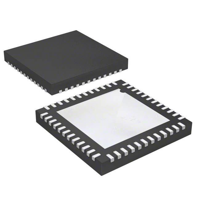
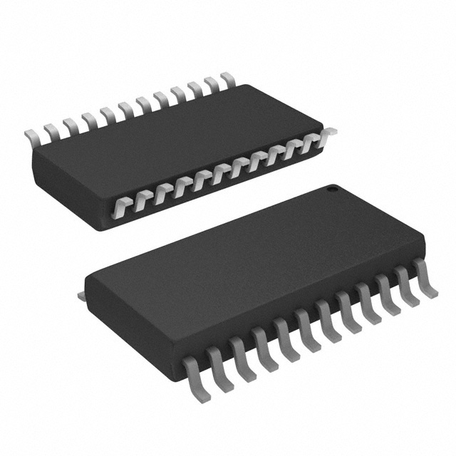
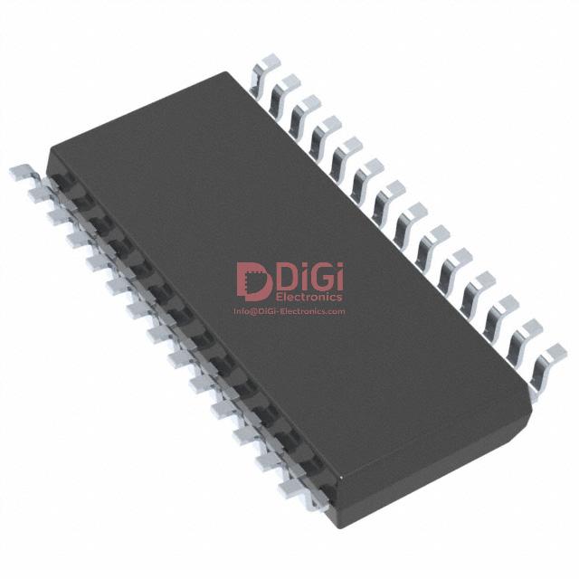
Package details: SO-28 implementation of STDRIVE601TR
The SO-28 implementation of the STDRIVE601TR exemplifies a strategic approach to compact, efficient gate driver integration. This package leverages a small footprint to enable high-density board layouts, which directly support the ongoing industry trend toward miniaturization without sacrificing electrical performance or assembly reliability. The SO-28 form factor balances lead pitch and body size, facilitating streamlined routing for both power and signal traces while minimizing electromagnetic interference concerns, especially in densely populated multi-layer PCBs.
Mechanical data and recommended PCB land patterns cater to precision in footprint matching, which is critical during both the design and production phases. These data ensure alignment with standard pick-and-place equipment for surface-mount assembly lines, while also maintaining adequate solder joint integrity in manual rework or prototyping scenarios. Furthermore, ECOPACK compliance aligns with increasingly stringent supply chain requirements, reflecting a shift toward environmentally responsible sourcing and manufacturing—a factor now essential in both regulatory compliance and market acceptance.
The package’s thermal metrics form a foundational consideration for gate driver deployment in industrial environments. By quantifying junction-to-ambient and junction-to-board thermal resistances, designers can evaluate heat dissipation pathways and implement efficient cooling strategies. This enables confident specification of maximum switching currents and duty cycles without risking device degradation. In the context of compact motor drives or power inverters, maintaining thermal margins within the SO-28’s envelope directly impacts long-term reliability and field performance.
In practical application, SO-28’s geometry simplifies board stackup decisions and opens layout flexibility. For example, its straightforward lead configuration allows close placement to power MOSFETs, reducing gate loop inductance—a persistent engineering challenge at high switching frequencies. This mechanical proximity, paired with robust thermal anchoring, supports the STDRIVE601TR’s intended performance envelope across diverse industrial automation and precision control scenarios.
A notable advantage emerges in the trade-off between package compactness and assembly resilience. The SO-28’s design preserves adequate standoff to minimize solder bridging, even as landing pads are optimized for space savings. This geometry, therefore, is particularly valuable when balancing aggressive product miniaturization targets with yield optimization and post-assembly inspection constraints.
Overall, the SO-28 implementation of STDRIVE601TR fosters a robust intersection of efficient thermal design, manufacturability, and system integration flexibility. This underlines its suitability for next-generation industrial hardware, where size, environmental compliance, and assembly reliability are now baseline requirements.
Potential equivalent/replacement models for STDRIVE601TR
Evaluation of replacement models for the STDRIVE601TR hinges on marrying system-level requirements with device-specific characteristics. Triple half-bridge gate driver ICs operate in diverse applications such as inverter stages, brushless DC motors, and power conversion, where topology alignment and protection mechanisms are fundamental. A methodical approach to screening equivalent devices begins with voltage rail compatibility; while the STDRIVE601TR supports 600 V rails, alternative drivers frequently offer different maximum ratings. This affects not only breakdown robustness but also insulation, creepage distances, and board-level layout constraints.
Gate drive current capability directly impacts the speed and assurance of MOSFET or IGBT switching. Differences in source/sink drive strength influence electromagnetic interference, thermal performance, and overall system reliability. Propagation delay and timing determinism represent another pivot—subtle variations here result in altered deadtime requirements, switching losses, and potential shoot-through events in multi-phase topologies. Integrated protections are multifaceted: UVLO constrains power-on stability, smart shutdowns or comparator-based logic respond to fast fault events, while programmable deadtime and interlocking hardware mitigate cross-conduction. These features are often implemented differently across vendors; assessment should extend beyond datasheet specs to architecture, fault behavior under dynamic load, and field failure modes.
Input logic level compatibility must match upstream controller standards—either TTL, CMOS, or custom thresholds dictated by isolation or ASIC outputs. The package format, lead pitch, and environmental ratings (moisture sensitivity, RoHS compliance) determine manufacturability, rework strategy, and long-term reliability under thermal stress. Matching the STDRIVE601TR’s particular blend of features often leads to candidate parts within the STDRIVE family—cross-verification of pinout, thermal characteristics, and protection logic is advisable. Cross-vendor equivalents require a formal comparison matrix, with score-weighted priorities such as electrical overstress endurance, propagation detach delay jitter, and logic threshold hysteresis, not only to verify spec alignment but also to surface latent incompatibilities.
Experience shows that transitioning to alternatives demands a disciplined prototyping cycle. Critical differences often emerge only after board-level evaluation: under transient overcurrent, variance in shutdown response time may induce unpredictable behavior. Subtle differences in deadtime programmability can manifest as either benign power losses or catastrophic device failure—hence, iterative bench testing under representative load conditions is essential before volume adoption. It is prudent to factor in not just the technical overlap but also procurement lead times, supply chain stability, vendor application support, and long-term product obsolescence risk.
Ultimately, direct replacement for the STDRIVE601TR is feasible in principle, but tightly constrained by application-specific tolerances across voltage, timing, protection, and logic integration. Layered examination—beginning with base electrical characteristics, proceeding through timing and input interface, then environmental and supply chain implications—yields a robust basis for selection. Optimized outcomes arise from integrating datasets across datasheet specifics, failure analysis feedback, and operational context, ensuring both theoretical equivalence and practical viability.
Typical engineering scenarios and application examples of STDRIVE601TR
STDRIVE601TR serves as an integral solution for high-performance, three-phase motor control within the realms of industrial automation, precision robotics, and compact inverter designs. Its architecture is centered on offering synchronized, high-frequency gate drive capabilities, essential for achieving tight control of switching sequences in brushless DC and AC induction motors. The inherent signal integrity and timing precision directly translate to superior torque management and reduced losses during dynamic load changes—a key factor in applications where precise movement and responsive speed regulation are critical.
In densely designed power inverter circuits, the rapid switching performance of STDRIVE601TR minimizes conduction and switching losses while enabling efficient use of space. The device operates reliably even in electrically noisy environments, protecting both the drive circuitry and the motor against fault conditions like short circuits and over-temperature scenarios. Its advanced diagnostic outputs help streamline fault detection and enhance system uptime, an advantage when deploying automation equipment subject to continuous or mission-critical usage.
Integrated bootstrap diodes play a vital role in minimizing external circuitry, which not only simplifies PCB trace routing but also reduces parasitic inductance and susceptibility to voltage overshoots. The matched propagation delays between channels further support balanced switching—a necessity for three-phase drives to prevent current imbalances and lower the risk of shoot-through events. These attributes frequently deliver tangible improvements in reliability, particularly in systems where thermal cycling and long operational lifetimes are required.
In practical deployments, careful layout strategy around the STDRIVE601TR yields enhanced EMI performance, due to minimized loop areas and effective separation between high- and low-voltage domains. Techniques such as optimal placement of decoupling capacitors close to supply pins, paired with meticulous ground plane design, maximize noise immunity and support the robust switching edges expected in high-frequency PWM applications. Empirically, platforms designed around this IC reflect increased system robustness, with enhanced motor start-up characteristics and more predictable performance across wide temperature and voltage ranges.
A distinctive insight emerges from observing STDRIVE601TR’s consistent performance in inverter modules with variable supply rails. Its inherent flexibility allows for seamless integration into both cost-sensitive and high-end applications, bridging the gap between simplified bill-of-materials and demanding functional safety requirements. Leveraging these characteristics, designers can accelerate time-to-market for industrial drives, with confidence that protection, efficiency, and scalability have been engineered directly into the heart of the motor control subsystem.
Conclusion
The STDRIVE601TR, engineered by STMicroelectronics, targets precision in three-phase motor and power-switching architectures. Its foundation lies in high-voltage capability, with operational thresholds up to 600V, and peak output currents tailored to drive both N-channel MOSFETs and IGBTs—key for variable speed drives, servo systems, and compact inverter topologies. The device integrates level-shifting gate drivers, providing both high-side and low-side channels with matched propagation delay. This minimizes dead-time uncertainty and advances synchronous drive efficiency, directly translating to improved motor control accuracy and energy utilization.
Built-in protection schemes, such as under-voltage lockout, shoot-through prevention, and fault diagnostic signaling, offer operational resilience against common electrical stressors. These mechanisms actively safeguard against destructive conditions, like phase-to-ground shorts or unforeseen supply sags, reducing both development time and post-deployment field failures. Gate driver logic provides flexibility through TTL/CMOS compatible input thresholds, supporting seamless interface with a wide spectrum of microcontroller or DSP families. This electric-level harmonization eliminates custom interface circuitry, ensuring rapid platform migration and system scalability.
From an integration perspective, the STDRIVE601TR’s thermally efficient surface-mount packaging streamlines PCB layouts in dense control electronics. Its compact footprint is favorable in space-constrained applications such as robotics, appliance drives, or tightly packed industrial controllers. The device architecture also supports bootstrap operation for high-side channels, enabling reliable performance in demanding switching regimes without excessive bill-of-materials overhead.
Practical implementation experience illustrates that leveraging the device’s comprehensive fault feedback reduces time spent on test-bench validation by quickly pinpointing integration issues early in prototyping. Its inherent gate-driving symmetry minimizes cross-conduction risk, which is critical when tuning fast-switching power stages where subtle timing mismatches often result in device stress or EMI spikes. In field-deployed systems where uptime is non-negotiable, the STDRIVE601TR’s robust feature set lowers unscheduled maintenance rates, especially in harsh industrial environments with variable loads and supply anomalies.
The assessment of this device versus alternatives pivots on careful mapping of system requirements: balancing fault-tolerance demands, logic-level compatibility constraints, and the thermal budget of the final design. In application areas where fast protection response and minimal logic overhead are prioritized, the STDRIVE601TR demonstrates distinctive strengths. Its convergence of drive capability, protection intelligence, and integration readiness presents an optimized pathway for future-proof motor drive and inverter solutions in the evolving landscape of industrial automation.