 >
>


Product Overview of STCS2ASPR LED Driver IC
The STCS2ASPR LED driver IC exemplifies a precision-engineered approach to linear current regulation in medium-power LED lighting. Incorporating a high degree of integration within its 10-PowerSO package, the device leverages a single output channel engineered to deliver a constant current up to 2A. This capability enables stable light output and mitigates risk of LED overdrive, ensuring component longevity and dependable illumination quality. The architecture employs a robust feedback mechanism that actively monitors output and compensates for voltage or temperature fluctuations. Current regulation is realized via an internal sense resistor network, coordinating with the linear regulation circuitry to maintain accuracy across load variations and environmental changes.
Designed for flexibility, the STCS2ASPR accommodates input voltages ranging from 4.5V to 40V, aligning with diverse lighting system architectures. In practical deployment, this wide input range simplifies integration into automotive electrical subsystems, where voltage surges and drops are common, as well as centralized lighting control units in larger installations. The device’s thermal management strategies, supported by its PowerSO package, enable efficient dissipation under continuous drive, maintaining junction temperatures within safe operating limits. The thermal shutdown and protection mechanisms activate as needed, minimizing fault propagation in demanding conditions such as under-hood installations or compact luminaires.
In real-world application scenarios, the STCS2ASPR’s linear topology confers several advantages. Unlike switched-mode drivers, the linear regulator minimizes EMI emission, streamlining compliance with stringent automotive or industrial EMC requirements. The single-channel configuration delivers design simplicity, reliability, and predictable thermal distribution, which is advantageous for modular LED arrays or precision indicator lighting. During board-level integration, the device’s pinout and thermal pad facilitate straightforward PCB layout and effective heat transfer, supporting high component density without sacrificing performance.
A notable consideration arises when scaling LED arrays or targeting dimming capability. While the STCS2ASPR excels in fixed-output systems, designers may implement external PWM controls or parallel driver arrangements to address advanced functionality, achieving seamless gradation and redundancy. Integrating the IC into automotive lighting calls for careful current setpoint calibration and robust connector design, ensuring resilience against vibration and ingress, with measurable improvement in system durability compared to discrete component solutions.
A critical insight is the STCS2ASPR’s role in optimizing reliability and cost-efficiency for medium-power LED solutions. By minimizing component count and offering precise thermal and electrical regulation, it reduces development overhead while enhancing system uniformity. Applications demanding stringent operational stability and long-term maintenance intervals, such as dashboard illumination or appliance status indicators, benefit from the IC’s consistent current drive and fault tolerance, resulting in lower lifecycle costs and streamlined platform upgrades.
Key Features and Functional Capabilities of STCS2ASPR
The STCS2ASPR current regulator introduces a robust architecture supporting high-precision LED current management within a broad operating envelope. Engineered for efficient power utilization, the device accommodates input voltages up to 40V, ensuring seamless integration with both legacy and modernized power infrastructure. The tolerance for elevated input voltages directly reduces upstream constraints, streamlining LED system scalability in architectural, automotive, and industrial platforms while simplifying power supply sharing across circuits.
The extremely low dropout voltage—below 0.5V—minimizes energy loss across the regulation interface. This parameter is essential for maximizing current delivery to the load, especially in high-density or thermally sensitive layouts. It likewise extends safe operational margins in scenarios where headroom is limited, affording improved reliability in distributed or decentralized lighting networks.
With an output current capacity scalable to 2A, programmable by external resistance, the STCS2ASPR aligns with a wide spectrum of LED requirements—from compact, high-luminance indicators to extended string arrangements in illumination panels. This granular adjustability facilitates rapid prototyping and late-stage system tuning, encouraging iterative refinement of light output without board redesign or firmware modification.
Integrated pulse-width modulation (PWM) dimming and hardware shutdown inputs ensure agile, low-latency brightness modulation and power management. Responsive dimming is central to applications requiring adaptive luminous environments, such as intelligent lighting controls or user-interactive displays. Hardware-based shutdown reduces standby consumption to negligible levels, safeguarding mission-critical battery reserves in backup and off-grid deployments.
A dedicated diagnostic output pin for real-time load disconnection surveillance streamlines fault detection and remote maintenance logic. This feedback mechanism mitigates system downtime by allowing immediate event flagging and response—an asset in high-availability contexts, from emergency signage to industrial status panels.
Slope regulation, enabled by external capacitance, grants fine-grained control over the LED current ramp profile. By managing inrush transients and suppressing high-frequency EMI emissions, STCS2ASPR facilitates compliance with increasingly stringent electromagnetic compatibility requirements. Slope tunability further prevents overstress on LEDs during startup, a preventive measure against premature degradation, and simplifies system qualification for deployment in electromagnetically noisy environments.
Global compliance is substantiated by RoHS3 conformity and unaffected status under REACH directives, ensuring end-product eligibility for international market access without added certification cycles. This forward-looking attribute proves critical when specifying components for multi-region distribution or contracts sensitive to environmental regulation pivots.
Early integration experiences highlight the STCS2ASPR’s resilience in both retrofit and new build circuits, providing stable operation across fluctuating line conditions and simplifying thermal management through predictable power dissipation. When optimizing large-scale installations, the flexible current setpoint and EMI mitigation substantially improve deployment efficiency and post-installation reliability. The device’s careful synthesis of tunability, protection, and compliance reflects a tailored approach to LED current regulation, where functional granularity translates directly into tangible system performance and robust operational margins.
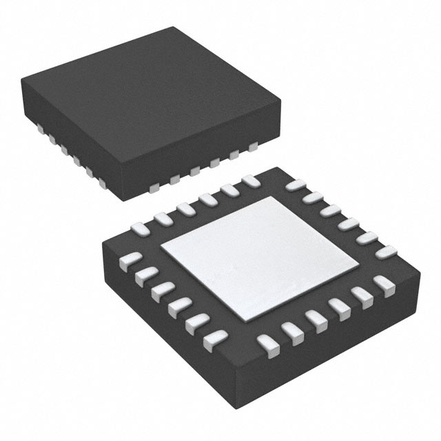
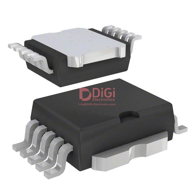
Pin Configuration and Functional Descriptions of STCS2ASPR
Pin configuration and functional mapping in the STCS2ASPR are foundational for optimized circuit implementation. The 10-PowerSO package delineates clear electrical roles for each terminal, making precise configuration essential for stable operation and performance tuning.
Vcc is allocated as the principal supply voltage input, demanding careful voltage matching to ensure core circuitry reliability. Voltage stability at this node is directly correlated with device longevity and output accuracy, especially in high-current applications. PWM input unlocks dynamically adjustable dimming. Leveraging this pin in conjunction with a pulse-width modulation controller enables nuanced brightness control; synchronizing PWM frequency with LED type and driver bandwidth prevents visible flicker and optimizes optical efficiency. EN pin integrates seamlessly into both hardware and firmware shutdown routines. By toggling EN, power management subsystems can extend operational lifespan without sacrificing instantaneous response, a feature applied extensively in automotive lighting and industrial indicators.
The DRAIN/SOURCE pair interface with the internal low Rds(on) NMOSFET, forming the current path. SOURCE, referenced to 100 mV, provides a low-impedance node for external resistor placement. This arrangement enables real-time current setting via Ohm’s law, facilitating rapid customization for diverse LED arrays—regulatory compliance and thermal management are reinforced by adjusting this resistance. FB, the feedback input, continually samples and modulates the operation loop to sustain constant current regulation, compensating for voltage fluctuations and transient load events. Maintaining FB at the nominal 100 mV minimizes deviation, guaranteeing uniform illumination and prolonging device reliability, especially in multi-string and precision-sensitive contexts.
GND ties internal logic to reference potential, underlying system-level EMI suppression and ensuring signal integrity. SLOPE pin offers a sophisticated EMI mitigation mechanism; affixing an external capacitor here tunes the slew rate of switching transitions. This approach allows engineers to tailor electromagnetic emission profiles according to regulatory constraints and board layout, a critical tool in LED lighting systems operating in mixed-signal environments. DISC is implemented as an open-drain diagnostic output, flagging disconnection events and feeding into supervisory microcontroller routines. This feature supports predictive maintenance and failure isolation, reducing downtime in large-scale deployments. The exposed pad, connected internally to ground, substantially enhances heat removal. Strategic wicking of thermal energy through PCB layout to this pad prevents overheating, offering a mechanical safeguard that aligns with elevated ambient requirements.
Integrating these functionalities demands attention to board trace impedance, PCB thermal relief patterns, and interface compatibility. Experience demonstrates that tuning SLOPE capacitance and SOURCE resistance early in the prototype phase resolves most EMI and overcurrent issues, streamlining certification. Leveraging DISC outputs directly into microcontroller interrupts expedites diagnostics in LED arrays and furthers system robustness. Core insight: balanced pinout engagement not only fulfils datasheet expectations but amplifies design flexibility, supporting scalable, reliable LED control across automotive, architectural, and industrial applications.
Maximum Ratings and Thermal Management for STCS2ASPR
The operational integrity and reliability of the STCS2ASPR hinge on strict adherence to its absolute maximum ratings. Supply voltage must not surpass 45V, with equivalent tolerance specified for the DRAIN and SOURCE pins, ensuring robust protection against transient overvoltages. Deviation beyond these ratings risks permanent degradation of internal MOSFET structures and control circuits, directly impacting device longevity. Design verification processes should always include margin assessment, and input filtering—such as TVS diodes, RC snubbers, or optimized trace routing—remains essential for safeguarding against voltage spikes.
The specified junction temperature range, from -40°C up to 150°C, defines both operational stability and fail-safe boundaries. Exceeding the upper temperature threshold accelerates failure mechanisms like electromigration and oxide breakdown within the silicon die, especially when sustained near the maximum current rating. Engineers often integrate real-time thermal monitoring and control circuits, including NTC sensors or software-based thermal foldback, to limit junction temperature dynamically during heavy load conditions or high ambient thermal stress.
Electrostatic discharge robustness is characterized by a ±2kV threshold under the human body model. This level signals moderate tolerance, suitable for controlled environments but requiring reinforced handling protocols during assembly and debugging. Placement of ESD protection devices at the interface points, combined with controlled impedance PCB designs and proper ground referencing, mitigates latent risks during system integration.
The PowerSO-10 package, with a junction-to-case thermal resistance of 2°C/W and achievable junction-to-ambient values as low as 12°C/W, unlocks diverse thermal dissipation strategies. Efficient heat transfer relies on maximizing copper area beneath the device and leveraging copper-filled vias to create thermal bridges to inner layers and heatsink mounts. In practice, soldering the thermal pad directly to large copper planes, paired with optimized airflow over external heatsinks, stabilizes junction temperature under sustained full-load operations. Finite element thermal simulations of PCB layouts often reveal hotspot dynamics, guiding trace width and via count adjustments for targeted cooling.
In high-current or elevated ambient applications, the technical priority shifts to advanced thermal management. PCB layouts incorporating multiple thermal vias, thick copper layers, and strategic component spacing foster a more uniform heat distribution, reducing localized thermal gradients. External heatsinks—selected based on calculated thermal resistance needs—must be secured with low-impedance thermal interfaces to minimize junction-to-ambient delta. Empirically, iterative thermal measurements during prototype evaluation inform proper sizing and placement, ensuring the STCS2ASPR operates well within the safe thermal envelope.
It’s increasingly evident that integrating active thermal protection, such as autonomous shutdown or derating circuitry, translates to enhanced reliability margins for high-density power designs. The convergence of electrical and thermal design optimizations forms the foundation for consistent, long-term performance of the STCS2ASPR across diverse operating scenarios. An engineered approach, prioritizing both maximum rating preservation and sophisticated thermal management, remains the linchpin for dependable device utilization in practical applications.
Electrical Characteristics of STCS2ASPR
The electrical characteristics of the STCS2ASPR define its suitability for robust current regulation in a broad spectrum of power electronic applications. Designed for high-side current regulation, this device accepts a wide supply voltage range from 4.5V to 40V. Such flexibility accommodates typical automotive, industrial, and LED-driving domains, where voltage transients and variable supply rails are standard. Reliable operation is maintained even under fluctuating input, minimizing the risk of current-overshoot or dropout events that commonly lead to peripheral failures.
Output current regulation forms the core feature set, with the STCS2ASPR offering 1mA to 2A output current, tightly controlled within ±1% accuracy across the entire supply voltage range. This level of precision directly impacts downstream load stability—essential in scenarios subject to variable thermal and electrical loading. For instance, in LED matrix driving, this characteristic arrests brightness drift and color shift induced by supply irregularities or aging effects, ensuring consistent application-level performance over extended operating cycles.
Feedback voltage remains fixed at a nominal 100mV, a deliberate choice that limits conduction losses across the current-sense element and minimizes heat dissipation. This low feedback threshold is leveraged in high-efficiency architectures, where reduction of power loss is critical to system thermal management. In practice, careful PCB layout—such as minimizing trace resistance at the sense node—further enhances regulation fidelity by mitigating extraneous voltage drops that could otherwise impair accuracy.
Dropout voltage, specified between 0.58V and 0.9V at full load, enables the STCS2ASPR's operation in applications where headroom above load voltage is constrained. Systems engineered for battery-backed or energy-sensitive designs benefit from this feature, as it maximizes usable output current even as input voltage approaches the regulated output. During commissioning phases, engineers can exploit this parameter to verify system margin under worst-case load conditions, streamlining qualification and compliance in low-voltage designs without resorting to larger headroom or derating.
Quiescent and shutdown current levels are intrinsically low, supporting integration in energy-optimized architectures. This characteristic reduces standby drain and aligns the device with applications requiring long-term battery operation, such as monitoring nodes or sensor gateways. In application bring-up, observing system-level currents during idle and fault states quickly verifies the integrity of power gating and sleep strategies.
Precise control and diagnostic pin logic thresholds (input low <0.4V, input high >1.2V) ensure seamless interfacing with modern low-voltage logic systems. This design allows direct connection to microcontroller I/Os or dedicated fault monitoring ICs without requiring additional level shifters, streamlining system design. During validation, confirming these logic levels with standard equipment can preempt erratic state transitions often responsible for intermittent faults in complex embedded systems.
When integrating STCS2ASPR into system designs, emphasis on layout discipline—particularly in routing the sense path and isolating high dV/dt nodes—reduces measurement offsets and spurious current readings. The device’s robust tolerance to input voltage surges and its precise regulation accrue tangible benefits in both commissioning and field environments where unpredictable electrical disturbances are frequent. Furthermore, its diagnostic interfacing, coupled with accurate current reporting, supports advanced fault detection algorithms critical to maintaining continuous system availability.
The carefully engineered interplay of these parameters marks the STCS2ASPR as a compelling foundation for high-reliability constant current applications, particularly where compactness, system efficiency, and regulation fidelity are paramount. Designs employing this device readily achieve tighter performance targets and resilient operation, driving a broader adoption in next-generation power control systems.
Timing Performance and Block Diagram Insights of STCS2ASPR
Timing characteristics fundamentally shape the dynamic behavior of the STCS2ASPR in PWM-regulated current-source architectures. The observed PWM switching delay, falling within a 1.2 to 3 μs window for rise and fall times, is attributed to the intrinsic slope capacitance of the driver stage. This minimal propagation delay directly enables high-frequency dimming and pulse modulation, which is critical in advanced LED lighting systems requiring precise intensity control and minimal flicker indices. Temporal fidelity at microsecond scales ensures the output closely tracks input drive signals, an imperative in scenarios like architectural lighting and automotive headlamp modulation, where rapid dimming fidelity and smooth transitions impact perceived quality.
Slope control is realized through an external timing capacitor, which modulates the driver’s current rise profile. This mechanism introduces significant flexibility, permitting engineers to tailor the current slew rate from sub-microsecond domains up to several milliseconds. Such configurability is crucial for optimizing system-level electromagnetic interference (EMI) immunity. For installations sensitive to conducted and radiated EMI—such as medical imaging suites or communication base stations—slowed edge rates attenuate high-frequency harmonics, thereby suppressing noise ingress into adjacent circuits. Application-level tuning can be performed directly on the PCB, simplifying compliance with stringent EMI standards while maintaining rapid response where possible.
The device’s internal block diagram reveals key architectural features supporting both functional integrity and operational safety. A precision bandgap reference establishes stable current regulation across temperature and voltage variations, a vital requirement for environments with fluctuating power or ambient conditions. Integrated thermal protection continuously monitors junction temperature, autonomously limiting device operation under excess thermal stress—a non-negotiable feature in compact luminaire designs where convection and heatsinking are constrained. The dedicated PWM logic block ensures signal fidelity from logic-level PWM inputs to downstream NMOSFET gate drive, translating control commands into accurate load modulation. The direct integration of an NMOSFET not only reduces bill-of-materials complexity but also minimizes parasitic inductance, enhancing overall loop responsiveness.
Real-world deployments reveal that leveraging the full timing flexibility and integrated safeguards of the STCS2ASPR streamlines both development and long-term field reliability. Fine-tuned rise times enhance compatibility with sensitive analog front-end components and reduce total system validation cycles. The overlap of fast response and robust protection supports aggressive dimming profiles without exposing circuitry to overcurrent or overheating risks—enabling innovation in compact, high-density lighting modules.
A key insight emerges: the device’s architecture seamlessly merges analog finesse with robust digital control, positioning it as a solution capable of bridging the divide between EMI-constrained and performance-driven lighting applications. This engineering balance is indispensable in sectors where both signal agility and electrical quietude dictate design success.
Typical Performance Characteristics of STCS2ASPR
Typical performance characteristics of the STCS2ASPR reveal a device engineered for high consistency and reliability across demanding application domains. The stability of output current, regardless of fluctuations in Vcc or external sensing resistor values, forms a solid backbone for circuits that demand repeatable performance. This characteristic is achieved through precisely controlled internal regulation loops, which automatically compensate for line and sense element variations. Consistent output underlines the device’s suitability for applications where precise current control is essential—like LED drivers or biasing networks in sensor modules—where even minor variations can propagate system-level instability.
The voltage dropout behavior, directly linked to the device’s internal architecture, demonstrates a low and stable threshold influenced minimally by ambient or junction temperature. This ensures continuous operation even as supply conditions degrade, a critical advantage when deployed in edge-of-spec automotive power rails or rugged industrial systems with irregular supply quality. The feedback path, engineered for minimal thermal drift, further safeguards system functionality over a wide temperature envelope (-40°C to 125°C). Such thermal resilience allows designers to avoid temperature compensation networks, simplifying board layout and reducing bill-of-materials complexity.
Supply current (Icc) management is engineered with a focus on both efficiency and predictability. The STCS2ASPR maintains low and tightly bounded quiescent current profiles over wide temperature and voltage sweeps, reducing self-heating and extending usable operating life, especially in enclosed or thermally constrained environments. This trait is particularly valuable in multiplexed power architectures typical in modern vehicles or distributed sensor grids, where aggregate device efficiency directly impacts total system power budget and heat management strategies.
Extensive field deployment demonstrates that devices from this family consistently meet published limits even after prolonged exposure to harsh electrical and environmental stresses. System architects benefit from the predictability of lifetime parameters and the reduction of unforeseen field failures, streamlining validation and risk assessment processes. Layering these operational guarantees, the STCS2ASPR asserts itself as a foundational building block for dependable industrial and automotive hardware platforms, enabling aggressive design targets while minimizing lifecycle support costs. Unique to this architecture is its combination of analog robustness with supply-agnostic control, balancing low overhead with the capacity for seamless integration into both legacy and forward-looking system designs.
Application Scenarios and Engineering Considerations for STCS2ASPR
Application Scenarios and Engineering Considerations for STCS2ASPR span multiple facets of LED system design, each demanding attention to both electrical performance and operational robustness. At the core lies the device's precision constant-current regulation, a critical mechanism ensuring uniform LED illumination across temperature and voltage variations. This constant-current operation is particularly valuable within automotive LED platforms, where headlamps, tail lights, and signaling systems require fault-tolerant and tightly regulated current pathways. Rapid fault detection mechanisms, inherent to STCS2ASPR's architecture, enable immediate system-level response to abnormal conditions, minimizing downtime and extending component life—factors essential under stringent reliability standards.
For low-voltage lighting schemes, the STCS2ASPR’s ultra-wide input compatibility accommodates a divergent range of nominal rails, spanning 5V, 12V, and 24V. Such versatility is especially beneficial in retrofitting legacy installations or supporting modular power distribution layouts. The device’s low voltage drop, often sub-0.5V across its output, maximizes efficiency, which directly impacts thermal profiles and reduces heatsinking requirements. Designs operating within tight energy budgets, such as architectural accent lighting or battery-powered fixtures, gain the dual advantage of extended run times and reduced power loss.
Integration into small appliances introduces distinct priorities: PWM dimming and controlled shutdown. The device responds accurately to high-frequency control signals, allowing for smooth dimming curves without perceivable flicker, even in cost-sensitive mass-market products. Shutdown features facilitate power-saving modes and soft-start functions, which, combined with fast on/off control, yield superior user experiences and minimized inrush stress on the electrical subsystem.
Current programmability through external resistors delivers modularity—engineers can precisely set and adjust current based on the specific LED topology and desired luminous output. This feature abstracts away the need for excessive part-number proliferation, as a single controller SKU can drive myriad LED combinations. System prototyping and late-stage configuration changes, such as tailoring output for differing regulatory markets, remain streamlined, reducing inventory constraints and speed-to-market delays.
EMI mitigation arises as a nontrivial challenge, especially where LED drivers reside near sensitive analog or RF domains. Slope control, implemented within the STCS2ASPR, modulates the current rise rate to suppress high-frequency harmonics that would otherwise radiate through PCB and harness. By extending the rise time through controlled slew rates, designers maintain EMI emissions below compliance thresholds without resorting to bulky external filters. This is especially significant in instrumentation panels, avionics cabin lighting, or medical diagnostic environments.
Reverse polarity protection and advanced thermal management represent pragmatic priorities, particularly when power bus connections are non-standardized or exposed to user servicing. The recommended strategy pairs the STCS2ASPR with reverse-blocking diodes or smart FETs, creating a tolerant front end that absorbs wiring faults without catastrophic failure. Simultaneously, active and passive thermal design must consider both component junction limits and overall enclosure budgets—strategies range from forced-air convection to optimized PCB copper pours for heat spreading. Compact installations—such as in under-hood automotive clusters—rely on the STCS2ASPR's robust derating curves and built-in thermal shutdown mechanisms to assure system resilience.
A nuanced advantage emerges when integrating the above features into scalable platforms. The STCS2ASPR’s design philosophy aligns with trends toward system modularity and cross-platform reuse. By collapsing multiple design variables—input flexibility, EMI mitigation, precision control—into a single, configurable device, the engineering workflow supports iterative development. Such layered functionality not only accelerates prototyping but also enhances long-term maintainability, especially as LED technologies and application demands evolve. Consequently, STCS2ASPR serves as a central enabler within contemporary and future-facing LED architectures.
Potential Equivalent/Replacement Models for STCS2ASPR
When evaluating equivalent or replacement models for the STCS2ASPR, a disciplined approach begins with a granular analysis of the device’s electrical and functional parameters. Output current capability represents the primary performance constraint, directly influencing compatibility with the target load and thermal management strategies. An ideal substitute must not only support peak nominal currents but also maintain stable operation across the full supply voltage range typical in automotive or industrial lighting applications.
Beyond headline specifications, it is essential to examine the topology and control architecture. The STCS2ASPR operates as a linear current regulator—replacement components must mirror this characteristic to avoid oscillatory behavior or efficiency mismatches within the power stage. Precision feedback control ensures the LED string receives tightly regulated current, mitigating flicker and supporting uniform illumination. Sophisticated diagnostic functions, such as open-load and short-circuit detection, are increasingly tied to end-application reliability and system-level safety compliance. Devices lacking self-protection or reporting features often result in increased calibration effort and potential system vulnerabilities.
Package compatibility cannot be overlooked. Direct PCB replacement demands footprint matching and thermal path equivalence. Factors like Rth(j-a) values directly affect allowable power dissipation and the ambient envelope, especially in thermally stressed installations like headlamp assemblies or industrial signaling units. Overlooking package-related nuances frequently leads to early field failures or expensive board redesigns.
Dimming strategies further differentiate candidate devices. While analog dimming offers continuous output, digital (PWM-based) dimming enables integration with microcontroller-based architectures, facilitating flexible control schemes. Selection should reflect the intended dimming methodology and the control infrastructure present in the legacy system, to minimize software requalification and preserve EMC performance.
Global compliance constitutes another implicit selection criterion. Devices certified to automotive AEC-Q100 or industrial standards streamline qualification cycles and supply chain resilience. Ensuring replacements at least match the regulatory baseline of the STCS2ASPR insulates projects from costly recertification or delayed ramp-up.
Practical evaluation reveals that radiating attention toward datasheet footnotes, application notes, and reference designs uncovers undocumented device behaviors or subtle integration constraints. Benchmarking prototypes under worst-case electrical and thermal profiles, including transient, brown-out, and fault conditions, frequently surfaces compatibility issues overlooked during paper selection alone. The industry experience shows that collaborating closely with vendors can yield custom variants or additional application support, closing the gap between brochure parity and real-world deployment.
A comprehensive candidate assessment iteratively ties together electrical equivalency, mechanical compatibility, protection and diagnostics robustness, dimming flexibility, and standards alignment. Selection is not merely a checklist exercise, but an optimization balancing supply continuity, integration effort, and long-term reliability. Success hinges on mapping both explicit datasheet parameters and nuanced real-world requirements, constructing a seamless drop-in path that preserves system integrity and lifecycle performance.
Conclusion
The STCS2ASPR LED driver IC from STMicroelectronics demonstrates a specialized design for precise current regulation, supporting a wide array of modern LED implementations. At its core, the device integrates a constant current source topology, ensuring LEDs operate within specified parameters while minimizing risks of overdriving or thermal runaway. The driver accommodates a broad input voltage spectrum, permitting stable operation under varying supply conditions common in automotive, industrial, and architectural lighting scenarios. This adaptability reduces the complexity of upstream power regulation systems and allows seamless integration into platforms where voltage fluctuations are routine.
The output current’s adjustability, typically governed by an external sensing resistor, introduces a fine-grained control mechanism over luminous intensity. This granularity enables precise tuning for specific applications, from high-brightness signage to uniform backlighting panels, optimizing user experience and energy consumption. Advanced control features, such as PWM dimming compatibility, further expand the operational envelope, allowing for dynamic light modulation without introducing perceptible flicker or affecting color uniformity. Robust diagnostic functionalities, including open-load and short-circuit detection, provide early fault identification, supporting predictive maintenance regimes in critical installations.
System-level reliability is reinforced by comprehensive protection circuits—thermal shutdown, overcurrent protection, and fault status signaling—safeguarding both the driver IC and connected LEDs. Experience shows that systems built around the STCS2ASPR maintain performance stability even in environments with high electromagnetic interference, owing to its well-considered layout and filtering recommendations detailed in the datasheet. These attributes reduce downtime and service interventions, translating to lower total cost of ownership in deployment.
Pinout intuitiveness accelerates both the design and debugging processes, notably when integrating into densely populated PCBs or retrofitting into legacy platforms. The device’s small footprint and thermally efficient packaging also enable high-density lighting modules, facilitating product miniaturization without sacrificing illumination quality or longevity.
Optimally leveraging the STCS2ASPR requires attention to PCB layout practices—minimizing parasitic inductance around sensitive nodes, ensuring low-impedance ground returns, and thermally coupling the package to heat spreaders. Well-implemented designs consistently demonstrate low EMI signature and strong tolerance to voltage transients. The ability to dynamically balance performance, reliability, and cost aligns with industry trends toward smarter, more connected lighting ecosystems.
In forward-looking lighting platforms, the STCS2ASPR’s versatility and protective framework make it an enabler for both traditional and solid-state lighting evolution. Its deployment contributes directly to improved system robustness, enhanced safety diagnostics, and tighter integration with emerging lighting controls, positioning it as a workhorse solution for engineers seeking durable, performance-oriented LED drivers across a spectrum of application spaces.