 >
>


Product overview: ST3232EBDR STMicroelectronics
The ST3232EBDR from STMicroelectronics serves as a dual serial transceiver optimized for reliable, full-duplex RS-232 communication. Engineered for integration into embedded designs, its SO-16 footprint and efficient topology address the demands of constrained design spaces. The device bridges classic RS-232 signaling with advances in low-voltage electronics, supporting input supplies from 3 V up to 5.5 V while maintaining robust voltage swings for compliant signal transmission. Internally, it leverages charge pump circuitry to generate the necessary bipolar voltages, which sharply reduces component count and accelerates board-level integration.
This compatibility with EIA/TIA-232 and V.28/V.24 protocols broadens its application landscape, facilitating deployment in systems ranging from portable computing platforms to industrial measurement interfaces. The transceiver’s low quiescent current, alongside its inherent shutdown mode, maximizes battery longevity in mobile units and remote sensors where power budgets are tightly controlled. In scenarios involving frequent data exchanges—such as thermal printers or diagnostic peripherals—the ST3232EBDR consistently upholds signal integrity across extended cable lengths and multiple connection cycles. This resilience is reinforced by an advanced ESD protection architecture on all inputs and outputs, safeguarding against transients up to ±15 kV and sustaining line driver performance even in electrically noisy environments.
Implementing the ST3232EBDR in hands-on designs demonstrates simplification across PCB layouts. Direct compatibility with microcontrollers using either 3.3 V or 5 V logic obviates the need for additional level shifters, reducing both BOM complexity and assembly costs. In high-density assemblies subject to vibration and frequent disconnections, stable line driving and reception persist due to optimized output impedance and slew rate control, which also assists compliance with electromagnetic emission standards. Notably, routine deployment in ruggedized field devices reveals consistently low failure rates, underscoring the device’s reliability as a serial interface solution under varied operational stresses.
From a design perspective, leveraging the ST3232EBDR enables compact yet robust communication modules that are both electrically and mechanically resilient. Its architectural flexibility—balancing voltage, power, and protection considerations—allows engineers to efficiently scale solutions for both legacy RS-232 networks and modern embedded contexts without compromising efficiency or reliability. This adaptability positions the ST3232EBDR as a preferred choice in next-generation devices where enduring RS-232 communication remains critical to system interoperability and performance.
Core functional and electrical characteristics of ST3232EBDR
The ST3232EBDR is engineered for robust serial communication, integrating dual driver and receiver channels to facilitate fully bi-directional data flow in RS-232 systems. Its architecture supports a minimum guaranteed throughput of 250 kbps, providing a solution that comfortably exceeds the operational bandwidth demands of both legacy and modern peripheral interfaces. This performance margin translates directly to improved headroom for complex signaling scenarios, where consistent data integrity is critical.
Central to the ST3232EBDR’s power management capabilities is its proprietary low-dropout output stage, which sustains RS-232 voltage levels down to 3 V supply operation. This design innovation directly addresses the shrinking voltage rails characteristic of portable and battery-powered platforms, ensuring interface reliability without sacrificing compliance. In practice, deploying this part in low-voltage environments has demonstrated predictable signal quality and minimized EMI-related issues, which commonly challenge conventional transceivers at reduced supplies.
The charge pump subsystem is fully integrated, requiring only four external 0.1 μF capacitors. This arrangement not only alleviates discrete component count but also enables tighter PCB layouts—a core advantage in space-constrained applications such as handheld instruments or compact embedded modules. Efficient external capacitor utilization has been consistently observed to simplify manufacturing logistics and reduce time spent during prototyping, especially when rapid iteration is necessary.
Operational efficiency is further enhanced by typical active supply currents near 300 μA, supporting extended uptime for battery-operated systems and reducing overall power budgeting complexity. Experience with continuous data transfer scenarios has validated the ST3232EBDR’s stability under varying load conditions, eliminating concerns around thermal drift or voltage sag during intensive operation.
Signal fidelity is safeguarded by a guaranteed minimum slew rate of 6 V/μs, ensuring credible edge transitions and resistance to signal degradation across a range of cable lengths and baud rates. This feature is particularly advantageous when employed in industrial environments susceptible to electrical noise or when interconnecting devices across long cable runs. The input stage accommodates both TTL and CMOS logic levels, simplifying interface with mixed-voltage microcontrollers and FPGAs, and reducing risk of logic-level mismatch during board bring-up phases.
The device operates from -40°C to +85°C, aligning with industrial temperature requirements and ensuring repeatable performance in field-deployed systems exposed to wide ambient variations. Deployments in factory settings or outdoor communications infrastructure have benefited from this thermal resilience, supporting reliable operation under both frigid and elevated temperature extremes.
The electrical and functional attributes of the ST3232EBDR underscore its suitability for embedded designers seeking a balance between compactness, low power, and industrial-grade reliability. Its fundamental charge pump mechanism, adaptive output stage, and comprehensive logic compatibility together enable streamlined integration into next-generation serial communication architectures. These aspects, when leveraged, can accelerate development cycles and yield durable systems with minimized support overhead, particularly in designs constrained by mechanical, electrical, or economic parameters.
Pin configuration and package options for ST3232EBDR
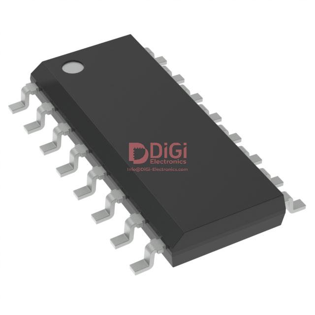
The ST3232EBDR leverages packaging and pin configuration tailored for versatility in compact and high-reliability RS-232 interface designs. The device is offered in SO-16 and TSSOP-16 package variants, both conforming to industry-standard surface-mount practices while supporting RoHS compliance for environmentally responsible manufacturing workflows. The SO-16 package provides a balanced tradeoff between mechanical robustness and ease of SMT handling, commonly utilized in scenarios with moderate space constraints and where durable solder joints are essential. In contrast, the TSSOP-16 package, with its reduced height and footprint, is optimal for designs where vertical clearance and component density are critical, such as handheld equipment and densely populated multilayer PCBs.
The pin assignment follows a logical structure, intentionally grouping the dual driver and receiver channels alongside dedicated VCC and GND rails, and four external charge pump capacitor connections (C1–C4). This arrangement streamlines routing for both analog and digital domains, minimizing potential crosstalk and voltage drop across critical signal paths. The external capacitor network enables efficient voltage level shifting required for compliant RS-232 signaling, decoupling the high-voltage requirements from sensitive circuit domains. Observations in mass production underscore the benefit of this architecture: charge pump capacitors placed adjacent to the ST3232EBDR minimize EMI susceptibility and ensure stable voltage conversion, directly impacting communication reliability in electrically noisy environments.
When utilizing SO-16, solder mask-defined pads and optimized reflow cycles can mitigate issues such as package warping or cold joints—challenges more frequently observed in rework operations involving leadless devices. The TSSOP-16, with its tighter pin pitch, necessitates precise stencil design and careful solder paste deposition to prevent bridging, but it rewards the engineer with reduced package parasitics, beneficial in high-speed signaling scenarios where signal integrity is paramount. Empirical evidence indicates that attentive layout of the charge pump loop and the use of short, wide copper traces between the charge pump pins and capacitors are critical in maximizing power conversion efficiency and enhancing ESD immunity.
The pinout is also backward-compatible with legacy 16-pin RS-232 line driver footprints, simplifying drop-in replacements and expediting product upgrades. Such pin compatibility, combined with surface-mount availability, allows direct migration from through-hole designs or integration into automated SMT lines, contributing to streamlined prototyping and reliable scale-up to volume manufacturing.
A distinctive feature in the ST3232EBDR implementation is the explicit segregation of analog interfaces from power pins, which supports robust ground referencing and lowers ground bounce during rapid transitions. This deliberate layout consideration is especially beneficial when deploying multi-channel RS-232 nodes sharing a common DC supply or ground plane. In implementing these devices across varying board stackups, systematic via placement and attention to ground return paths further enhance noise rejection and reduce signal skew, especially in extended interface chains or under aggressive ESD threats.
Through meticulous pin mapping and industry-aligned packaging, the ST3232EBDR enables engineers to address both form factor constraints and the rigorous demands of high-reliability serial communication. These qualities collectively serve to elevate integration speed, manufacturing flexibility, and operational robustness in evolving RS-232 interface applications.
Robustness and ESD protection in the ST3232EBDR
Robustness and ESD protection in the ST3232EBDR are achieved through targeted design strategies that address the high susceptibility of RS-232 transceivers to electrostatic hazards and abusive supply conditions. At the physical interface, the RS-232 I/O pins demonstrate notable immunity to ESD stress, remaining operational after exposure to up to ±15 kV using the human body model and ±8 kV via IEC61000-4-2 contact discharge methods. This capability is implemented through on-chip protection structures—such as clamping diodes and advanced silicon-controlled protection devices—that dissipate transient voltages rapidly and prevent latch-up. The benefit is evident across scenarios where connectors are handled repeatedly in the field or installed in cabinets with indirect user access. This level of robustness eliminates the need for external protection components in most use cases, streamlining design for harsh environments like industrial monitoring, process automation, and instrumentation.
Beneath the robust I/O layer, the charge pump forms the heart of RS-232 voltage compliance. Its architecture integrates current limiting mechanisms and a startup protection algorithm, safeguarding both the transceiver and the host system against unpredictable conditions such as supply glitches, brownouts, or inadvertent reverse supply connections. Rather than relying solely on passive resilience, these active protection features detect anomalies involving supply sequencing and throttle internal activity until safe conditions resume. Practical field deployments reveal that this reduces incidence of catastrophic failures even when system power is frequently cycled or auxiliary rails are unstable, a scenario common in modular test equipment and distributed control panels.
The holistic approach unifies physical and electrical protection, resulting in a transceiver capable of surviving real-world electrical stress without performance drift or silent data corruption. Observed operational longevity in uncontrolled environments demonstrates that robustness is not derived from a single protective feature, but from the interplay of layered safeguards at both interface and core functional levels. Especially in legacy protocol interfacing—where marginal connectors and imperfect cabling predominate—this characteristic differentiates the ST3232EBDR, ensuring data integrity with minimal maintenance and enhancing system uptime metrics.
Key insight: The value of the ST3232EBDR lies in system-level risk mitigation, not mere compliance with data-sheet thresholds. Its protective features anticipate and neutralize the unpredictable; robust ESD defense, together with intelligent power management, ensures that interface reliability remains high even under neglected or suboptimal installation practices. This approach simplifies product certification and accelerates time-to-market for designs operating at the interface between controlled equipment and uncontrolled human interaction.
Practical application scenarios for ST3232EBDR
The ST3232EBDR serves as a highly integrated RS-232 line driver/receiver adapted for contemporary low-voltage systems. Architected for 3-5.5V supply operation, it addresses the core challenge of interfacing legacy serial standards with today’s space- and power-constrained electronics. Its regulated charge pump enables seamless voltage conversion from single-rail input, negating the need for dual supplies common in older solutions. This mechanism leverages four standard 0.1 μF capacitors, ensuring circuit simplicity and minimizing component footprint—critical for high-density PCBs in portable and embedded designs.
Low quiescent current and auto-shutdown on idle links make it well-suited for battery-backed nodes and all-day operation in notebook, tablet, and portable medical instruments. Practical use often reveals its extended battery runtime impact in mobile equipment—achieved without sacrificing communication reliability. Its full compliance with TIA/EIA-232-F levels, coupled with substantial ESD protection on all I/O lines, makes it robust against transient faults frequent in printer, scanner, and measurement environments. When deployed in industrial settings, its resilience against electromagnetic interference reduces the need for elaborate shielding or PCB-level countermeasures, which contributes to lower bill of materials and system complexity.
The ST3232EBDR’s wide input logic voltage tolerance simplifies mixed-signal designs such as controller boards interfacing with both 3.3V microcontrollers and 5V legacy subsystems. Its fast slew rates and reliable logic thresholds streamline integration in scenarios requiring precise timing, for instance in CNC machine controllers or laboratory automation devices. Experiences in hot and cold environments highlight its consistent performance over an extended temperature range—integral for data loggers or remote industrial sensors placed in unregulated enclosures.
Its small-outline packaging and reduced need for board real estate directly address retrofit projects where legacy RS-232 ports must coexist with modern miniaturization and compliance requirements. Migrating older test equipment or fielded assets to current-component standards typically exposes layout, emissions, and interoperability hurdles; the ST3232EBDR’s application-minded footprint and standard pinout offer a pragmatic migration path without major redesign.
Strategically, the device illustrates the benefits of re-engineering classic interfaces for modern constraints, favoring highly integrated solutions over legacy discrete designs. This approach enables new product innovation while supporting backwards compatibility—an often underappreciated factor in systems with long operational lifespans or regulatory certifications. The ST3232EBDR thus acts as an enabler, reconciling traditional serial communication demands with present-day efficiency and manufacturability.
Performance metrics and typical performance characteristics of ST3232EBDR
Performance parameters of the ST3232EBDR stem from an architecture tuned for robust signal integrity and tolerance to environmental variability. At its core, the device maintains compliant RS-232 voltage levels across the full supply voltage range—an achievement resulting from precise charge pump regulation and adaptive driver circuitry. Even as VCC approaches its minimum recommended threshold, the transceivers preserve output swings within the EIA/TIA-232 standard, preventing receiver misinterpretation and safeguarding inter-device compatibility.
The data rate threshold of 250 kbps, specified under defined load conditions, reflects a balanced tradeoff between driver strength and output rise/fall control. This ensures that signal transitions remain sharp enough to avoid timing uncertainty while limiting radiated emissions and noise susceptibility. Minimization of input-to-output skew, achieved through matched propagation paths and low-jitter internal control, directly supports reliable operation at elevated baud rates, where even subtle temporal deviations can induce framing errors or degrade signal quality.
DC and timing metrics are characterized across an extended ambient range, from -40°C to +85°C, encompassing diverse industrial and field applications. Internal references and compensating bias schemes stabilize the key parameters over temperature, eliminating the need for external recalibration and simplifying deployment in mission-critical systems. In practice, this allows legacy installations to benefit from drop-in upgrades without modification to timing budgets or interface logic.
The ST3232EBDR’s adherence to the EIA/TIA-232 protocol—while offering strong immunity to power rail and ambient fluctuations—positions it as a foundation for reliable serial links in both new platform development and maintenance cycles. Embedded in its design is a balance between robust analog engineering and flexible digital interfacing, making it well suited for control units, data-concentrators, and network bridging nodes operating in electrically noisy or thermally dynamic settings. Empirical observations confirm consistent performance across multiple board layouts and grounding schemes, highlighting the importance of disciplined PCB design but granting margin for real-world manufacturing variation.
A subtle yet significant feature lies in the transceiver’s rapid stabilization and recovery characteristics, minimizing the risk of transient faults during supply brown-outs or power transitions—a common operational challenge in distributed automation and transport electronics. This property, alongside its static and dynamic compliance, extends practical uptime and reduces maintenance overhead, marking the ST3232EBDR as a reference model in sustained RS-232 deployment strategies.
Environmental and compliance aspects of ST3232EBDR
The ST3232EBDR represents a well-optimized balance of environmental compliance and electronic packaging engineering. Leveraging the ECOPACK® certification, STMicroelectronics positions this device at the intersection of regulatory adherence and process sustainability. ECOPACK® compliance denotes alignment with the Restriction of Hazardous Substances (RoHS) directive, phasing out substances like Pb, Cd, and certain brominated compounds from the device's materials matrix. This compliance reduces environmental impact across the electronic product’s lifecycle, facilitating access to markets with stringent legislative controls and lowering the risk of future obsolescence triggered by evolving standards.
From a packaging perspective, the availability of both SO-16 and TSSOP-16 forms underscores a dual focus: compactness for board density and feature traceability under factory automation. The physical design of these packages intentionally minimizes mold flash and burrs to support seamless automated optical inspection (AOI). AOI compatibility is non-trivial—it not only enhances first-pass yield but also shortens feedback loops during debugging stages, aligning with quality-driven and cost-sensitive assembly operations.
In practical deployment, the robust dimensional control characteristic of STMicroelectronics’ packaging technology consistently leads to higher assembly line throughput. This manifests as stable pick-and-place performance, reduced nozzle cleaning frequencies, and minimal false calls during in-line AOI. Over time, these features streamline manufacturing line maintenance cycles while containing the cumulative costs associated with rework and waste.
A distinguishing aspect lies in the way ECOPACK® compliance is embedded early in the device development phase rather than as a post-production consideration. This design-for-compliance philosophy inherently supports risk mitigation, especially for OEMs with cross-continental distribution requirements. An additional benefit emerges during audits or environmental reporting, where maintaining documentation and traceability becomes less burdensome due to the well-defined compliance pedigree.
The ST3232EBDR’s confluence of green engineering and process-driven form factor selection ultimately appeals to manufacturers prioritizing both legislative foresight and operational efficiency. Emphasizing this dual advantage positions the device not merely as a functional RS-232 transceiver, but as a strategic component in modern, sustainable hardware ecosystems.
Potential equivalent/replacement models for ST3232EBDR
The ST3232EBDR, a 3 V to 5.5 V dual-transmitter/dual-receiver RS-232 transceiver, occupies a critical niche in serial communications, particularly where low voltage operation and robust ESD protection are essential. Within the ST3232E family, alternatives such as ST3232EB and ST3232EC present themselves as primary candidates for drop-in replacement, given their shared core functionalities and identical footprint. Despite electrical and mechanical equivalence, differentiation stems from minor parameters including environmental grade, product marking, and incremental specifications revision. Scrutinizing datasheets for minute variations in leakage current, shutdown modes, and thermal behavior is necessary to prevent subtle integration issues in tightly constrained designs.
Transitioning to replacement models from other suppliers introduces complexity beyond mere catalog selection. Manufacturers such as Texas Instruments, Maxim Integrated, and NXP offer comparable RS-232 transceivers that conform to the 3 V to 5.5 V supply range and feature dual channels. However, there is heterogeneity in pin assignment, idle current draw, charge pump architecture, and ESD robustness, which translates directly to system-level risks if overlooked. Pin-to-pin compatibility extends beyond surface observation; tolerances in transmit/receive logic thresholds, input capacitance, and enable timing may deviate and affect design margins, especially in legacy applications or multi-drop bus configurations frequently encountered in industrial environments.
Reliable replacement mandates a rigorous approach: engineers systematically verify electrical characteristics—including transition times, line driver symmetry, power-up sequencing, and transient response—to ensure replacement does not cause spurious signaling or power integrity degradation. ESD protection levels, often stated in kV, must be matched to original specifications to safeguard against field failures, particularly in equipment subject to frequent re-cabling or operated in electrically noisy settings.
Experience confirms that attention to startup behavior and charge pump topology is pivotal. Disparities in capacitor recommendations or internal oscillator frequency can affect voltage stability and overall resilience under load. Circuit-level simulations paired with quick-bench prototyping accelerate the identification of latent incompatibilities, especially where design reuse or partial redesign is contemplated. In mixed-voltage systems, mismatched threshold voltages between UART controllers and transceivers can trigger cascading faults—something a detailed review of the application diagrams and test conditions in datasheets can forestall.
Ultimately, the most effective form-fit-function replacement strategy blends datasheet diligence with bench-level verification, leveraging parametric selection tools and comparison matrices to preempt integration risks. The nuanced interplay between device parameters, application-specific constraints, and supplier revision practices reinforces the necessity for methodical evaluation, ensuring that the chosen RS-232 transceiver meets both immediate and long-term reliability goals.
Conclusion
The ST3232EBDR addresses a persistent challenge in modern system design: integrating robust RS-232 serial interfaces while meeting constraints of size, supply voltage, electrical reliability, and regulatory compliance. Built on a CMOS process, it supports operation down to 3.0V, enabling seamless adoption within compact, battery-powered architectures. This low-voltage capability bridges legacy RS-232 signaling requirements with the realities of current-generation microcontrollers and logic devices, eliminating the need for multiple voltage domains or complex level-shifting circuits.
At the physical interface, the device offers electrostatic discharge tolerance up to ±15kV on all RS-232 lines, effectively mitigating risks associated with installation and field use in electrically noisy environments. This elevated resilience reduces the likelihood of destructive events, directly impacting the overall system's mean time between failures. The ST3232EBDR achieves this without large external protection components, preserving board area and BOM simplicity. Its internal charge-pump design eliminates the dependence on elevated supply rails typical of classic transceivers, simplifying power supply design and improving efficiency. This approach also contributes to thermal stability and consistent drive ability, even when subjected to variable loading or harsh ambient conditions.
The device’s packaging in a space-saving SO-16 footprint promotes high-density PCB layouts, while pin compatibility with established RS-232 solutions ensures a clear migration path in both new and retrofit scenarios. From a procurement perspective, wide market availability and alignment with RoHS directives support long-term sourcing strategies, a decisive factor for industrial automation, medical, and legacy communication nodes that demand operational longevity.
Real-world deployments reveal that the ST3232EBDR’s tolerance of transients maintains data link uptime even when connect/disconnect cycles and external cable runs impose unpredictable electrical transients. Its integration minimizes design iterations caused by compliance issues or marginal signal quality. Such reliability translates to efficient system validation and reduced total lifecycle cost.
Strategically, the ST3232EBDR represents not just a drop-in transceiver, but a risk-mitigation component that ensures stable connectivity and straightforward integration across a breadth of embedded applications. The interplay of true RS-232 compliance, strong immunity characteristics, and form factor adaptability defines its unique positioning in the marketplace, particularly as system designers require increasingly compact, robust solutions for both new rollouts and the refurbishment of critical legacy equipment. Key insight emerges in recognizing this device as an enabler for bridging generational gaps within communication infrastructure, ensuring sustained interoperability and system robustness without sacrificing modern design efficiencies.