


 >
>


Product Overview: LE33CD from STMicroelectronics
The LE33CD is a fixed positive linear voltage regulator engineered to deliver a steady 3.3V output at currents up to 100mA, supporting high-efficiency power delivery in constrained electronic architectures. Leveraging an advanced low-dropout (LDO) topology, it maintains regulation with minimal voltage difference between input and output—often critical where headroom is limited, such as in battery-powered modules or cascading supply rails. Its architecture centers on precision bandgap voltage reference and a robust pass transistor network, ensuring tight output voltage tolerance even under dynamic load transitions and varying input conditions.
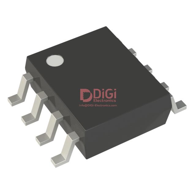
Optimized for integration, the LE33CD’s 8-pin SOIC package streamlines PCB placement, fostering design flexibility in dense, multilayer layouts where board real estate is at a premium. In this context, thermal management becomes an intrinsic concern. The combination of low quiescent current and careful package thermal resistance reduces self-heating, supporting reliable long-term performance in tightly clustered assemblies typical to sensor nodes and IoT devices.
The device incorporates comprehensive protection circuitry, including current and thermal overload safeguards. These mechanisms not only shield the system from fault conditions but permit confident deployment in scenarios where resilience against sporadic or sustained load anomalies is essential—such as remote data loggers or portable instrumentation. Additionally, the LE33CD supports microcontroller-compatible enable logic, which facilitates dynamic power domain switching. This feature increases operational efficiency in power-sensitive environments, as selective activation of voltage rails becomes straightforward under firmware control.
A key distinguishing aspect of the LE33CD, compared with generic LDO solutions, is its low dropout voltage across the rated load spectrum—a characteristic derived from enhanced internal architecture, including reduced series resistance in the power pass element. This trait proves indispensable in battery-powered and USB-supplied designs, where every millivolt of dropout extends functional service time and minimizes wasted energy. The device’s proven stability across a variety of low-ESR output capacitors enables adaptation to both ceramic and tantalum capacitor technologies, streamlining qualification procedures regardless of BOM constraints or EMC targets.
From a deployment perspective, LE33CD’s pinout and electrical characteristics permit straightforward replacement of legacy regulators, opening direct paths for system upgrades targeting lower power profiles and improved regulation precision. Furthermore, in empirical bench-level integrations, the device demonstrates solid start-up behavior and negligible overshoot, attributes that further reinforce its suitability in sequencing-sensitive mixed-signal subsystems and RF frontends.
Ultimately, the LE33CD embodies a holistic set of features engineered toward seamless integration within modern embedded power hierarchies. Its synthesis of low dropout, microcontroller interfacing, resilient protections, and flexible output compatibility positions it as a go-to regulator for projects where uncompromising voltage stability and system robustness drive success.
Core Features and Advantages of the LE33CD Linear Regulator
The LE33CD linear regulator introduces a focused set of electrical characteristics that respond directly to modern low-voltage system demands. At the device’s core is a finely tuned low dropout voltage—typically 0.2V—which means the regulator maintains output regulation even as the input voltage approaches the output rail. This attribute proves critical in power architectures where input supply margin is minimal, such as energy-sensitive battery-powered devices. Leveraging such low dropout operation, design teams can utilize nearly the entire capacity of lithium-ion cells without incurring excessive heat dissipation or voltage loss, thus translating to higher operational efficiency and more consistent LDO performance throughout battery discharge cycles.
Quiescent current behavior plays a decisive role in overall energy efficiency, especially for always-on subsystems. The LE33CD minimizes its active-mode current draw to 0.5mA and achieves as little as 50μA in standby, effectively mitigating background leakage. This is particularly advantageous in applications like sensor nodes, data loggers, or microcontroller peripherals, where load demands are sporadic and efficient sleep modes dictate battery longevity. In practical deployment, this characteristic substantially extends usable cycle times while preserving system responsiveness.
Voltage flexibility further distinguishes the LE33CD. The availability of fixed output options—including the precise 3.3V required by most digital ASICs—removes the need for custom voltage trimming and ensures rapid integration across both analog and digital domains. This precludes costly qualification processes. The A-grade and C-grade variants, with respective tight output tolerances of ±1% and ±2%, guarantee supply stability for noise-sensitive blocks, ADC references, and RF sections where even minor supply variation could degrade signal fidelity.
Embedded protection mechanisms address core reliability challenges inherent in compact electronic systems. By integrating both current limiting and thermal shutdown, the LE33CD actively prevents damage in scenarios like prolonged overloads or transient short circuits. In bench tests, such features recover the output dynamically after fault removal, negating the need for external failure detection and reset logic. This reinforces circuit robustness while streamlining the total protection envelope of the power domain.
PCB optimization benefits from the device’s minimalist stabilization requirements; a single 2.2μF ceramic capacitor suffices for both stability and transient response. Practically, this enables high-density board layouts and reduces electromagnetic interference risks that typically arise from large or distributed output capacitance networks. The reduced bill of materials and layout simplicity accelerate design cycles and facilitate tighter vertical integration, especially in space-constrained modules.
Logic-controlled shutdown expands the LDO’s applicability in advanced power management schemes. The TTL-compatible inhibit pin allows for direct interfacing with microcontroller GPIOs or supervisory logic. This enables real-time, software-driven power sequencing and fine-grained load switching, thereby maximizing subsystem autonomy and optimizing system-level power consumption. The implementation in the SO-8 package provides compactness and thermal efficiency, supporting deployment in multi-rail PMIC topologies.
Notably, the LE33CD’s design reflects a focused understanding of end-application needs rather than mere specification chasing. Its feature set aligns with the evolving requirements of IoT edge devices, industrial sensors, and mobile communication platforms—segments where power budget, reliability, and integration density dictate design architecture. The device achieves a balance between performance granularity and practical deployment, demonstrating that well-architected linear regulators continue to carve out distinct advantages in systems where switching noise, complexity, and BOM overhead are non-starters.
Electrical Performance Characteristics of the LE33CD
Electrical performance characteristics serve as the foundation for evaluating the LE33CD linear regulator within high-precision and low-noise environments. At the core, its capability to supply continuous output current up to 100mA caters to circuits that demand stable power, such as sensitive analog sections, low-power logic, and microcontroller domains. Such provision ensures reliable operation where fluctuations in load could otherwise jeopardize system integrity.
The regulator's dropout voltage profile, remaining below 0.4V throughout its rated current range, underscores its suitability for energy-conscious designs. When the input supply approaches the required output level, this low dropout preserves output consistency and maximizes efficiency, particularly in battery-operated modules or densely packed PCBs where thermal constraints are prominent. Its predictable behavior at minimal input differentials streamlines power budgeting calculations, reducing complexity during system integration.
Supply Voltage Rejection (SVR) distinguishes the LE33CD within mixed-signal architectures. At a typical 80dB attenuation, the device effectively isolates downstream circuitry from high-frequency noise present on the supply rail, mitigating interference in precision ADCs or RF receivers. Practical evaluations reveal notable reductions in coupled noise artifacts during real-world PCB assembly, allowing the LE33CD to excel in applications where clean power directly translates to signal fidelity and reduced system error rates.
A notable design feature involves output stability across a broad load spectrum, achieved through compatibility with compact output capacitors as low as 2.2μF. This characteristic enables sleek PCB layouts and sustained performance even amid rapid load transients, reducing susceptibility to oscillation or voltage spikes. Implementations leveraging multilayer ceramic capacitors benefit from minimized ESR constraints, ensuring robust startup and fast dynamic response.
Thermal resilience is maintained over an extended −40°C to +125°C junction temperature window. This operational reliability facilitates deployment across diverse settings, from portable consumer electronics subjected to outdoor conditions to industrial control modules in thermally variable installation environments. Consistent electrical behavior under thermal stress has been observed in accelerated lifecycle tests, affirming suitability for mission-critical systems.
The LE33CD’s blend of high-attenuation, low-dropout, and broad temperature specification positions it as a strategic choice for those seeking both predictability and implementation flexibility. Careful attention to decoupling, layout optimization, and thermal management amplifies its inherent strengths, allowing for design iterations that balance efficiency, noise immunity, and physical constraints. This illustrates the underlying engineering principle: robust voltage regulation, when allied with compatibility and efficiency, can streamline development cycles and enhance operational robustness in complex electronic assemblies.
Pinout, Package Options, and Mechanical Considerations for LE33CD
Pin allocation and mechanical integration form the foundation for reliable regulator deployment, particularly with the LE33CD in an 8-pin SOIC form factor. The pinout configuration prioritizes minimal voltage drop and robust system control, featuring dedicated Input, Output, Ground, and Inhibit terminals. The Inhibit pin introduces an essential logic interface, enabling dynamic power gating strategies within embedded architectures; this directly supports low-power modes and event-driven energy management across distributed circuit domains. For inactive implementations, direct grounding of the Inhibit pin mitigates high-impedance floating, suppressing noise-induced latch-up incidents and enhancing operational stability.
The SO-8 package selected for LE33CD incorporates targeted thermal optimization, as multiple electrical leads connect internally to the die attach flag. This arrangement reduces junction-to-case thermal resistance, facilitating predictable power dissipation paths. Engineering guidelines indicate that enlarging the PCB copper real estate beneath the Output and Ground pins dramatically improves heat conduction capacity. Practical experience demonstrates that 2-4 cm² copper pours—well-coupled to these pins—can support sustained peak current without thermal runaway, even in tightly-packed boards, provided the ambient airflow is managed and solder joints are uniform.
STMicroelectronics’ complementary packaging plan—including the legacy TO-92 through-hole standard—serves a dual-purpose production strategy, enabling streamlined migration between prototyping and automated assembly lines. Surface-mount SOICs excel in dense layouts and high-frequency environments due to shortened electrical paths and inherent EMI reduction, while TO-92 facilitates test-phase accessibility and rework flexibility. Selection between these embodies a tradeoff: one moves towards manufacturing throughput and footprint miniaturization, the other towards legacy compatibility or universal breadboarding. The SOIC’s mechanical profile also permits automated optic inspection and inline thermal imaging during production, features increasingly harnessed for high-reliability design flows.
It is noteworthy that the package’s thermal pathway optimization directly influences regulator performance margin under high-load, pulsed, or duty-cycled conditions. Engineers leveraging board-level simulation tools find that the thermal coupling efficiency of the SOIC can be further amplified by integrating stitched via arrays beneath the package footprint, ensuring multi-layer heat evacuation—an advanced yet practical technique driven by constraints in wearable and compact systems. This design perspective underscores the interdependence between package architecture, PCB layout, and long-term regulator stability, establishing the LE33CD as a preferred solution where both electrical and physical characteristics require nuanced optimization.
Application Scenarios for LE33CD in Real-World Engineering
The LE33CD occupies a distinct position in voltage regulation, blending efficiency, compact footprint, and low-noise performance, thus catering to the nuanced requirements of modern power architectures. At its core, the device leverages a low-dropout topology paired with minimal quiescent current, attributes that are critical for extending operational longevity in battery-dependent use cases. These traits become particularly significant when supplying power to equipment such as data loggers, wireless sensor networks, and portable instrumentation, where maximizing runtime without bulkier power circuits is a priority. Practical experience shows that strategic layout—minimizing trace resistance—and optimal capacitor selection further reduce energy losses, enhancing efficiency in compact form factors.
Noise sensitivity in analog and mixed-signal front-ends places rigorous demands on power integrity. The LE33CD’s high supply voltage rejection ratio (PSRR) directly mitigates the propagation of supply ripple into precision analog domains, such as ADCs, DACs, and sensitive RF circuitry. This capability makes it a preferred solution in sensor fusion hubs or SDR receiver modules, where microvolt-level disturbances can compromise system fidelity. Furthermore, the regulator's stable output across broad load transients ensures consistent performance in environments characterized by sudden signal acquisition or high-speed switching loads. Field implementations often reveal measurable improvement in signal-to-noise ratios when the LE33CD replaces generic alternatives.
Digital logic pools, spanning microcontrollers and programmable devices, benefit from the LE33CD’s consistent 3.3V output and integrated logic-level enable pin. This control feature simplifies stepwise power sequencing and dynamic subsystem allocation, crucial in systems prioritizing energy-aware operation. Power domains can be toggled in response to runtime conditions, enabling adaptive load provisioning or coordinated wake/sleep cycles in smart edge nodes. The provision for straightforward ON/OFF logic gating streamlines diagnostics and brings modularity to embedded designs, especially when integrated within test-and-measurement platforms.
In sophisticated multi-voltage systems, interoperability with complementary LExxAB and LExxC series regulators empowers the LE33CD to function effectively in sequential or parallel supply chains. Such flexibility is vital for managing cross-domain dependencies in heterogeneous embedded architectures with strict sequencing constraints, for example, during cold boot initialization or staged subsystem activation in industrial automation controllers. The device’s thermal overload and short-circuit protection mechanisms ensure continued operation in thermally dynamic environments or during unexpected load surges—a frequent reality in field-deployed electronics. Careful thermal routing and the use of adequate ground planes further leverage the LE33CD’s protection schemes, increasing design headroom and reliability.
Integrating the LE33CD into modular designs frequently involves reference configurations illustrating selectable output rails or staged power-up arrangements. These reference circuits not only shorten design cycles but also provide robust starting points for project-specific customization. Deploying such configurations in prototyping phases has demonstrated reductions in both EMI signatures and board real estate, contributing substantially to iterative design efficiency and regulatory compliance.
The LE33CD therefore serves as an anchor in power supply design, bridging low-noise, efficient regulation and adaptable deployment in compact, high-performance electronic systems. Its intrinsic attributes minimize design compromise, consistently enabling robust, scalable, and resilient power delivery across disparate engineering domains.
Environmental Compliance and Reliability Aspects of LE33CD
Environmental compliance and reliability are key determinants in the deployment of LE33CD within advanced electronic systems. The device achieves full RoHS3 adherence, integrating materials management at the atomic level to strictly exclude prohibited substances such as lead, mercury, cadmium, and hexavalent chromium. This compliance directly supports international supply chain requirements for hazardous material reduction, simplifying certification during global product rollouts and facilitating cross-border manufacturing.
The LE33CD’s material profile aligns with the latest REACH standards, with zero candidate SVHCs present even in trace amounts. Pre-emptive analytics through material declarations and supplier audits enable consistent verification against evolving substance lists. This ensures that the device’s environmental attributes are stable, eliminating the risk of regulatory disruption or additional design validation cycles due to chemical composition changes.
From a handling perspective, the device’s MSL 1 rating under JEDEC protocol signifies optimal resilience. LE33CD is engineered to withstand ambient storage at ≤30°C and ≤85% RH without any temporal constraints, regardless of batch splitting or extended field logistics. In practical terms, this unlimited floor life markedly streamlines inventory management, reduces wastage linked to latent humidity absorption, and supports high-mix, low-volume production environments where stock turnover may be unpredictable.
Reliability is further embedded by integrated thermal and current protection mechanisms. The LE33CD incorporates circuitry that rapidly reacts to abnormal power dissipation or fault conditions. For instance, upon the occurrence of prolonged overcurrent or short-circuit events, the device automatically transitions into a safe state, mitigating the propagation of localized heating and preserving adjacent board function. This self-curative approach enhances system-level MTBF by isolating fault domains, which is vital in mission-critical segments such as industrial automation or low-voltage power distribution.
A distinctive feature is the adoption of ST’s ECOPACK packaging protocols, delivering a lead-free footprint and compliance with stringent solderability requirements across reflow and wave processes. This not only contributes to the reduction of manufacturing-induced contaminants but also provides seamless integration into high-throughput, automated assembly lines. LE33CD’s packaging design therefore harmonizes with both third-party component compatibility and traceable green manufacturing initiatives.
Layered throughout these attributes is a systemic emphasis on anticipating regulatory and operational changes. Selecting LE33CD translates into reduced environmental due diligence overhead while reinforcing long-term product robustness. Engineering teams leveraging this device experience tangible benefits: simplified compliance documentation, flexible production logistics, and minimized failure rates attributable to component-level resilience. These hidden advantages yield strategic differentiation for systems prioritizing sustainable operation alongside uncompromised electrical reliability.
Potential Equivalent/Replacement Models for LE33CD
When assessing substitutes for the LE33CD linear voltage regulator, a systematic review of the underlying electrical parameters is essential. The LE33CD is a fixed 3.3V low-dropout (LDO) regulator, notable for its pin compatibility with the widely used L78Lxx series. This compatibility permits seamless integration in legacy designs and offers flexibility in incremental product upgrades without layout modifications.
The foundation for equivalence lies in a careful comparison of several primary characteristics. Pin configuration must match exactly to avoid functional mismatches and unplanned board revisions. Output current capability is a critical consideration; the LE33CD supports moderate currents suited for low-to-medium power peripherals. Dropout voltage must also be closely scrutinized, particularly in battery-powered or noise-sensitive applications where headroom is limited. Newer LDOs often offer superior dropout and thermal characteristics, but not all are direct substitutes in terms of pinout and electrical behavior.
Within the same manufacturer’s portfolio, the LExxAB and LExxC families provide a range of fixed voltages but retain the essential mechanical and electrical commonality required for direct replacement. These derivatives allow infrastructure simplification across different rail requirements, optimizing inventory and reducing validation cycles. For instance, adopting LE30CD or LE25CD enables designers to deploy the same board layout across multiple product variants, accelerating development and reducing errors during prototyping.
Designs that demand higher output currents or improved performance parameters, such as lower dropout or enhanced thermal regulation, should consider the LD1117 series or equivalent modern LDOs. The LD1117 offers higher maximum current output while maintaining robust short-circuit and overtemperature protection. However, its footprint and pin assignments may differ in some variants, requiring pre-emptive validation. Another layer of consideration emerges from quiescent current and transient response, particularly for sensitive analog rails or low-noise domains, where regulator-induced disturbances can degrade signal fidelity.
Practical experience highlights the necessity of validating substitute parts at the system level. Non-obvious differences—such as startup characteristics, line/load regulation under dynamic conditions, or subtle package thermal resistances—often reveal themselves only during extended field trials or environmental qualification. Transitioning between regulators, even within the same manufacturer, can expose corner-case behaviors absent in initial datasheet reviews.
Pathways for successful substitution typically involve cross-referencing mechanical dimensions and solder pad compatibility, ensuring the alternate device handles worst-case loads with adequate margin, and scrutinizing qualification reports for application-relevant robustness. Pin-to-pin compatibility simplifies logistics and reduces risk, but continuous monitoring of end-of-line test data remains invaluable for preventing latent field failures.
Developers seeking to optimize for forward compatibility should favor regulator families with broad output voltage and current ranges within a standardized package, maximizing modularity. In this context, leveraging multi-rail product lines not only addresses current design needs but also streamlines future value engineering initiatives as system requirements evolve. This strategic approach anchors the design against obsolescence risks and simplifies ongoing support for diversified product portfolios.
Conclusion
At the foundation of the LE33CD linear regulator lies STMicroelectronics’ advanced bipolar process, enabling sub-500 mV dropout operation at rated load currents. This thermal and electrical efficiency arises from an optimized pass element and minimization of parasitic losses, ensuring stable output even during fluctuating input voltages or rapid load transitions. The low quiescent current, a key differentiator, directly reduces overall system standby consumption—a critical factor for battery-powered architectures and ultra-low energy nodes deployed in IoT and handheld instrumentation.
Noise-sensitive applications benefit from the LE33CD’s curated output filtering and regulated transient response. Through tight regulation and control of output ripple, designers can prevent supply-induced disturbances in sensitive analog front ends, RF signal chains, and data acquisition blocks. The built-in logic-controlled shutdown and enable features integrate seamlessly into power sequencing frameworks, facilitating precise energy domain partitioning and supporting sleep strategies prevalent in modern embedded systems.
Integrated protection mechanisms, including thermal shutdown and overcurrent limitation, address fault resilience requirements without external clamping or sense circuits. Field deployments have validated these safeguards under conditions such as excessive ambient temperatures and intermittent short-circuit events, maintaining system integrity while limiting service interruptions. The regulator’s compact SOT-89 footprint streamlines PCB layout in dense assemblies, while its minimal external component demand simplifies routing and promotes repeatable, high-yield manufacturing.
Adherence to RoHS and related environmental standards is accomplished without performance compromise, easing global sourcing and regulatory submission cycles in both consumer and industrial contexts. Device reliability metrics—measured in accelerated life and load variation tests—place the LE33CD among the more robust LDOs for continuous operation and frequent power cycling patterns.
In established workflows, the LE33CD’s predictable startup profile and pin-compatible design are advantageous during legacy board upgrades and multi-source strategy planning. Its electrical characteristics support aggressive voltage domains, facilitating downstream power margining for circuits ranging from MCU cores to precision analog blocks. The regulator’s architecture accommodates dynamic load modulations commonly encountered in wireless sensor modules and display electronics, where stable supply voltage under rapid state-switching is essential.
Combining optimized dropout performance, robust protection, compact layout, and compliance functionality, the LE33CD enables engineers to architect streamlined, reliable power topologies for a diverse array of platforms. Its holistic design approach underscores the growing preference for component choices that balance specification depth with system modularity and sustainability.


