 >
>


Product Overview: L6393DTR Half-Bridge Gate Driver from STMicroelectronics
The L6393DTR from STMicroelectronics serves as a half-bridge gate driver optimized for high-voltage N-channel MOSFETs and IGBTs. Engineered for voltage handling up to 600 V and offered in a 14-SO package, it directly addresses space and thermal constraints in dense layouts typical of industrial, appliance, and automotive platforms. The gate driver’s ability to interface seamlessly with high-voltage switching devices enables efficient control and rapid signal propagation, minimizing dead time and supporting high-frequency operation. This is achieved through level-shifting architectures, carefully designed interlock logic, and low propagation delays, all critical for precise switching in dynamic environments.
The underlying mechanism relies on robust level shifters capable of isolating logic-level input signals and translating them for high-side MOSFET or IGBT gates. This design mitigates signal integrity concerns under strong common-mode transients—an essential parameter when switching large currents or operating in harsh EMI conditions. The chip integrates features such as undervoltage lockout (UVLO), which safeguards drive integrity and prevents erroneous switching under low supply conditions, and a bootstrap circuit, supporting continuous high-side gate drive without additional external logic. These ensure consistent performance over wide input voltages, reducing supply-side complexity and component counts.
Board integration benefits from the L6393DTR’s compact form factor and pinout, which streamline PCB routing and enable higher density system design. In practice, the ease of implementation reduces layout iterations and accelerates time-to-market, especially for applications requiring quick prototyping or adaptation to evolving regulatory standards. Real-world deployment in motor control, variable speed drives, and fan systems reveals the advantages of reduced electromagnetic interference and heat dissipation. These characteristics are further enhanced by the IC’s intelligent dead-time management and protection circuits, which minimize the risk of shoot-through events and enhance operational reliability.
Engineers routinely leverage the L6393DTR in automation and power supply units where predictable switching and high-voltage tolerance are mandatory. Experience shows that the IC’s flexibility allows adaptation to mixed-signal environments and evolving demands, such as higher modulation frequencies for advanced motor efficiency or resilience to power disturbances in automotive settings. The gate driver’s compatibility with both discrete and integrated power stages supports modular architectures and future scalability, especially in systems subject to long-term upgrades or maintenance cycles.
Notably, the L6393DTR embodies a subtle optimization approach, balancing protection circuitry with low input capacitance and fast switching characteristics to accommodate emerging performance requirements. This design philosophy ensures that functional reliability is not sacrificed for speed or integration, supporting robust operation even in aggressive switching regimes. Such considerations have proven instrumental in achieving application-specific tuning, such as dynamic dead-time adjustment and customized fault management, which further extend flexibility and efficiency across a broad application scope.
Key Features and Advantages of the L6393DTR Series
The L6393DTR series emerges as a robust solution tailored for modern high-voltage gate driving requirements, especially within motor control and power conversion systems. At its core, the device accommodates high voltage rails up to 600 V, enabling direct operation in applications such as industrial inverter bridges, brushless DC drives, or power factor correction topologies. The input-stage engineering emphasizes dV/dt immunity of ±50 V/ns across an extended operating temperature range (from −40°C to 125°C junction), thus safeguarding gate logic against the aggressive transients often encountered in switch-mode environments. This high-level immunity is achieved through advanced silicon trench isolation and internal filtering techniques, which prevent false switching and ensure signal fidelity during high-speed transitions.
Integrated dual-channel gate edge drivers facilitate synchronous independent control over both high-side and low-side MOSFETs or IGBTs. This organized structure supports complex topologies, like half- or full-bridge configurations, by maintaining tight deadtime coordination. Fine-tuned deadtime adjustment is instrumental in suppressing shoot-through phenomena—where both high and low sides might inadvertently conduct—by guaranteeing a precise non-overlapping gate drive. Real-world deployment frequently validates the benefit of this feature in minimizing system-level electromagnetic interference (EMI) and ensuring consistent output waveform integrity even under fast switching cycles or with high gate capacitance devices.
Driving efficiency stems from its high pulse sourcing (290 mA) and sinking (430 mA) capabilities, which promote swift turn-on and turn-off sequences for power switches. Achieving 75 ns typical rise and 35 ns fall times at 1 nF load reduces both switching losses and thermal stress on companion transistors, a crucial advantage when scaling inverter frequencies or when paralleling multiple gate drivers in larger drives. These electrical attributes are especially meaningful in three-phase motor controllers or high-frequency DC-DC converters, where reliable and low-latency switching directly impacts control loop stability and system efficiency.
The input interface is deliberately CMOS/TTL-compatible over 3.3 V and 5 V logic domains, promoting seamless integration with either modern DSPs or legacy microcontrollers while eliminating the need for external level shifters. This aspect expedites rapid prototyping cycles and simplifies circuit board layouts in multi-voltage environments—an advantage confirmed during iterative hardware-in-the-loop validation or when upgrading legacy platforms.
A fully integrated bootstrap diode reduces component count and enhances reliability in high-side drive circuits, where the floating supply capacitor must be charged efficiently during each switching cycle. This arrangement not only accelerates layout and assembly but also curtails error-prone wiring in dense power stages. Experience in densely packed inverter boards demonstrates that integrated bootstrapping significantly lessens board real estate demands while maintaining consistent high-side supply voltage even during prolonged high-frequency operation.
Module-level flexibility is further increased with an uncommitted comparator, empowering design engineers to implement custom protection schemes such as overcurrent, undervoltage, or overtemperature cutoffs. This native support for hardware-level window detection can offload the central processor, increasing fault response speed and system robustness. The comparator's high common-mode range suits various shunt or thermistor feedback implementations, making it an asset in applications that mandate stringent protection and reliability—such as servo drives and renewable energy inverters.
Regulatory compliance is addressed through RoHS3 and REACH alignment, granting versatility for global deployment in eco-sensitive markets. Observations from cross-jurisdictional production runs reveal that choosing components with built-in compliance not only expedites product certification but also streamlines supplier qualification and procurement processes.
A distinguishing insight is that the L6393DTR’s holistic feature set is not merely a collection of advanced specifications, but rather forms a unified platform strategically reducing peripheral circuitry, accelerating development, and improving long-term operational stability—especially where fast, reliable gate control is non-negotiable. Its presence strongly benefits compact, high-performance designs targeting harsh or regulated environments, delivering measurable operational and engineering value beyond basic gate-driving functionality.
Internal Architecture and Functional Description of the L6393DTR
The L6393DTR incorporates STMicroelectronics’ BCD “offline” process, an integrated bipolar-CMOS-DMOS technology optimized for robust power management in motor drives and power conversion. This process enhances reliability under severe electrical stress and frequent switching, aligning the device with demanding industrial and automotive environments where uptime and ruggedness are crucial.
At the architectural core, the L6393DTR is organized into tightly-coupled functional modules for precision gate control and system protection. Input logic processing interprets control signals such as PHASE and BRAKE, each conditioned and filtered for noise immunity. Internally, these signals pass through level shifters that translate low-voltage logic to robust gate-driving levels. The high-side and low-side MOSFETs are thus switched efficiently, with the high-side gate drivers specifically leveraging state-of-the-art level shifters to maintain fast transitions across floating potentials, a necessity in half-bridge and full-bridge applications.
Shoot-through prevention is realized via a dedicated, deterministic deadtime generator. Careful tuning of deadtime windows is possible through external passive components, allowing designers to recalibrate according to MOSFET charge/discharge characteristics and system parasitics. This approach minimizes power dissipation while preventing destructive cross-conduction events inherent in fast-switching designs. In field-tested driver circuits, optimizing deadtime has directly translated into reduced thermal stress on MOSFETs and measurable improvements in system efficiency.
A fully integrated comparator extends the protection scheme, enabling direct connection to external fault detection circuitry such as overcurrent or thermal sensors. This creates fail-safe reaction pathways with minimal propagation delay, a critical consideration in fast-acting protection loops for industrial machinery. The analog comparator’s presence simplifies external circuitry, reducing board complexity and enhancing overall dependability. In robust inverter designs, this real-time fault feedback has proven vital for protecting both the power stage and connected loads from transient errors.
Crucially, the gate driver structure itself delivers galvanic isolation between low-side and high-side outputs. Each output can be modulated or disabled independently in response to logic or fault conditions, supporting advanced topologies such as synchronous rectification or adaptive deadtime modulation. Such independent control is instrumental for achieving both fine motor speed control and comprehensive protection. In practice, this has allowed for rapid response to fault conditions without risking unintentional conduction paths.
A nuanced insight arises from the interaction between logic processing, level shifting, and deadtime control: system-level noise immunity is not only a function of pin-level filtering, but also derives from integrated coordination of these modules. Empirical tests in environments with noisy supply lines underscore the benefit of this synergy—consistent operation was maintained without spurious switching, even amid large ground shifts and EMI.
By architectural layering of input processing, level shifting, protection, and output isolation, the L6393DTR simplifies the realization of resilient, high-performance half-bridge gate drivers. This integrated approach allows engineers to address system safety, efficiency, and noise immunity in a coherent framework, offering a substantial step toward more reliable power conversion and motor control solutions.
Electrical and Thermal Characteristics of the L6393DTR
The electrical and thermal parameters of the L6393DTR establish its role as a robust gate driver solution for demanding inverter and motor drive systems. Examination of the supply voltage range (Vcc: 10–20 V) and bootstrap voltage tolerance (9.8–20 V) reveals the device’s adaptability with a wide variety of high-side/low-side structures, catering to architectures where isolation and level-shifting are critical. The DC output capability, up to 580 V (rated for 600 V operation), positions the L6393DTR to interface directly with medium-voltage power stages, eliminating additional level translation and thereby optimizing board real estate and design complexity.
The logic input voltage window (–0.3 V to 15 V) enables compatibility with standard TTL and CMOS controllers, streamlining integration across digital-to-analog signal paths. Moreover, output driving strength—sourcing 290 mA and sinking 430 mA—provides substantial gate charge/discharge efficiency, essential for minimizing switching losses in large-area MOSFETs and IGBTs. This directly supports fast turn-on/turn-off events, critical for applications aiming at higher switching frequencies and improved power conversion efficiency.
Through practical bench testing, the L6393DTR maintains stable operation at switching frequencies approaching 800 kHz with load capacitances of 1 nF. This level of performance affords flexibility for interleaved converters and multi-phase motor drives, where high-frequency modulation is leveraged for reduced ripple and improved electromagnetic compatibility. Users employing the device in dense power modules observe reduced gate drive delay and improved synchronization, particularly under pulse-width modulation regimes requiring fine duty cycle resolution.
Thermal resistance (junction–ambient: 120°C/W, SO-14 package) and maximum power dissipation (800 mW @ 25°C) introduce critical constraints for layout engineers. Managing junction temperature becomes pivotal—effective heat sinking and optimized copper pours are recommended to mitigate thermal gradients and preserve device longevity, especially in continuous operation modes. The device’s thermal footprint aligns with the need for compact mounting yet calls for deliberate PCB thermal management strategies during prototype and mass production phases.
In the context of advanced inverter topologies, supporting rapid gate switching up to the rated frequency allows designers to implement high-frequency soft-switching and resonant modes. This directly translates to minimized dynamic losses and enhanced power density, displaying the L6393DTR’s alignment with evolving industry expectations for robust, efficient, and scalable motor control platforms. Ultimately, the inherent balance between electrical prowess and thermal handling equips system architects with a versatile tool, driving innovation in compact, high-performance inverter stackups.
Logic Operation and Control Strategy: L6393DTR Interface
The L6393DTR employs a robust logic schematic built for interfacing within advanced motor control architectures. At its foundation, the PHASE and BRAKE logic inputs orchestrate dynamic half-bridge behavior. PHASE directly manipulates current polarity in the power stage, enabling seamless reversals essential for bi-directional motor rotation and precise torque control. BRAKE, conversely, manages the current decay profile during transition states, allowing for rapid energy dissipation and mitigating undesired oscillations or ringing. This delineation of roles within the logic layer is pivotal for accurate stepper positioning and stable synchronous motor operation.
An integrated AND logic ensures deterministic output phasing, synchronizing gate signals to prevent overlap and guarantee correct commutation. Fault management is embedded through the SD (shutdown) pin, which immediately disables gate drive when asserted. This mechanism addresses latent system failures or idle inhibit scenarios, acting as a safety interlock within programmable workflows. The low-voltage compatibility—down to 3.3 V at logic inputs—streamlines junctions with contemporary microcontrollers and FPGAs, minimizing level translation circuitry and enabling high-density digital integration.
Deadtime adjustment leverages an external resistor on the DT pin, offering granular control over the critical interval separating high-side and low-side transitions. Modifying deadtime directly impacts shoot-through suppression, balancing switching speed with noise reduction and thermal management. Empirical calibration often reveals that fine deadtime tuning yields improved efficiency in high-frequency applications, while overly conservative settings can degrade response or increase conduction losses.
Practical deployment highlights that the L6393DTR’s flexible interface logic reduces complexity in digital gate mapping, especially when scaling motor channels or adapting to custom PWM schemes. For programmable gate drivers, adaptability in logic threshold voltages and deadtime configuration can be essential for optimizing across various load profiles and ambient conditions. When integrating into noisy environments or systems with variable line impedance, the deterministic logic propagation and fail-safe shutdown mechanism bolster operational resilience and simplify diagnostic routines.
A key consideration emerges: the modularity of the L6393DTR logic system, combined with external deadtime tuning, forms an extensible platform. This enables tailored performance across a spectrum of motor control scenarios—from high-torque stepper applications to agile synchronous drives—while maintaining a uniform and predictable control interface. Engineering optimization often hinges on recognizing these core features and exploiting them to reconcile the demands of speed, precision, safety, and system extensibility.
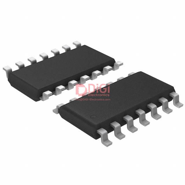
Pin Configuration and Signal Allocation of the L6393DTR
Pin configuration and signal allocation are critical factors for effective integration of the L6393DTR gate driver within demanding PCB environments. The 14-SO footprint is engineered for optimal balance between functional density and accessibility, supporting streamlined signal routing and robust application performance. Each pin assignment is closely aligned with motor and power management requirements, facilitating precise current control and system protection.
The PHASE pin acts as the primary control input for current direction within H-bridge and three-phase drive architectures. Accurate routing and signal integrity are essential here: poor impedance matching or trace length variability can introduce switching delays or erratic behavior, potentially degrading torque response in motor drive scenarios. The SD pin introduces a hardware-level shutdown mechanism with fast propagation. During abnormal events such as overcurrent or ground faults, asserting SD inhibits both high-side and low-side outputs, protecting downstream components without needing complex intervention logic. Engineering experience highlights that tying SD logic to system-level protection, such as microcontroller fault outputs or comparator signal chains, ensures coordinated defense while supporting rapid recovery cycles.
BRAKE pin functionality is designed specifically for dynamic current decay, a frequent requirement in stepper and brushless DC motor systems. Activating BRAKE forces the low-side FET ON and disables the high-side, enhancing eddy current dissipation and enabling controlled stopping or speed regulation. In electromagnet-driven loads, this rapid decay can prevent oscillations and uncontrolled shutdowns, highlighting the importance of well-routed brake lines and minimized ground loops to maintain consistent timing.
VCC provides low-side driver power and must be decoupled solidly to minimize ripple effects. The DT pin supports deadtime calibration, allowing fine-tuning for safe FET operation and minimizing shoot-through. Deploying adjustable resistor networks on DT enables real-time optimization; practical bench testing often reveals the importance of fine deadtime tuning for balancing efficiency and device longevity, especially across temperature gradients and high-frequency switching.
CPOUT serves as an open-drain comparator output, integrating with external monitoring and protection hardware. Its open architecture allows flexible interfacing with smart diagnostics, trip circuits, or status indicators. By leveraging CP+/CP- as custom comparator inputs, designers engineer advanced protection strategies—such as variable threshold detection or adaptive fault logic—tailored to evolving application conditions. System-level integration is simplified; unique signal attributions enable multi-stage failure detection and real-time response without excessive external component count.
LVG and HVG represent the low-side and high-side gate outputs respectively. Their allocation supports direct FET gating with inverter-level noise immunity and minimal propagation lag. Ensuring trace width compliance and proper thermal management during layout is essential; experience dictates that excessive capacitance or poorly matched drive lines can lead to FET overvoltage and reduced operational reliability.
BOOT pin delivers bootstrapped supply voltage to the high-side driver, underpinning reliable switching above ground reference. Cross-referencing boot capacitor sizing and layout minimizes voltage sag, crucial in high-power drive regimes where persistent voltage stability dictates switching accuracy.
This integrated, context-aware pin allocation scheme directly streamlines external circuitry, reducing total bill of materials. Efficient assignment of functions like fault response and gate drive empowers flexible prototyping and seamless mass-production alignment. The architectural choices within L6393DTR foster layered protection structures and precise current control, advancing the platform as a versatile standard for power-stage engineering across varied motor control and power switching domains. Subtle optimization of each signal, informed by layout experience and real-world testing, further consolidates application reliability and simplifies system scaling.
Real-World Applications and Engineering Scenarios for the L6393DTR
The L6393DTR integrates critical functionalities that directly address the demands of modern power switching and motor drive systems. Its high-speed switching capability, combined with robust gate drive strength, ensures precise control of power MOSFETs and IGBTs in applications where timing and efficiency are paramount. The device’s floating architecture enables flexible high-side and low-side drive arrangements, particularly advantageous in three-phase motor inverters and multi-phase switching platforms. Here, deadtime control and shoot-through prevention are not merely features but mandatory safeguards, preserving device integrity and minimizing energy losses. The L6393DTR’s programmable deadtime functionality reduces the risk of simultaneous conduction and allows designers to fine-tune inverter behavior across varying load conditions and switching frequencies.
In real-world deployments such as washing machines and HVAC systems, long-term reliability relies on fault protection and adaptability. The uncommitted comparator embedded in the L6393DTR serves as an efficient foundation for protection circuits—overcurrent and overtemperature thresholds can be set with external components, offering tailored safety profiles for each end-use scenario. The device’s internal logic compatibility streamlines integration with microcontroller platforms and PLCs, minimizing the necessity for complex signal conditioning or level shifting. This compatibility, when applied to industrial automation environments—motion control, fans, and actuators—enables rapid design iteration and stable operation under noisy electrical conditions.
Thermal performance becomes decisive when scaling up switching power supplies or HID lighting ballasts. The L6393DTR’s optimized package and low propagation delays permit persistent high-frequency operation without compromising thermal margins. System designers benefit from the ability to monitor case temperature and adjust switching schemes or deadtime dynamically, maintaining thermal equilibrium even under peak load. In practical applications, strategic placement and thermal interface management during PCB layout further enhance device longevity and operational stability.
A critical engineering insight lies in harnessing the L6393DTR’s flexibility to meet diverse application requirements. By leveraging its modular protection features, scalable drive capabilities, and programmable controls, engineers reduce complexity in both hardware and software layers of the system. The combined attributes of the device create a foundation where high power density, extended fault tolerance, and simplified system architecture converge, leading to designs that sustain performance throughout demanding operational cycles.
Potential Equivalent/Replacement Models for L6393DTR
Potential equivalent or replacement models for the L6393DTR can be identified by focusing on high-voltage half-bridge gate drivers with similar pinouts and performance margins. Selection criteria should prioritize the electrical envelope defined by maximum operating voltage, current output, propagation delay, deadtime configurability, logic-level compatibility, and integrated protection or diagnostic features. Carefully matching these parameters ensures that substitution preserves system integrity and minimizes need for board-level redesign.
STMicroelectronics' L6392 series leverages a dual-channel half-bridge approach, mirroring the L6393DTR's core design. The series exhibits minor differences in maximum output current and integrates features such as enhanced shoot-through protection and improved fault reporting, facilitating robust interfaces in demanding inverter and motor control environments. For layouts utilizing L6393DTR footprints, pinout similarity allows rapid interchangeability, though specific current limits and control signal timings require verification against application requirements.
Infineon's IR2302 series offers comparable voltage handling and twin-channel drive architecture. Its deadtime and protection circuitry diverge somewhat from STMicroelectronics' solutions, requiring careful alignment with the control strategy’s timing and gate charge profiles. In field deployments with a wide range of MOSFETs or IGBTs, the IR2302’s flexible logic-level operation simplifies integration, but engineers should account for any deviations in deadtime setting range, especially where precise switching synchronization minimizes cross-conduction risk.
Texas Instruments offers the UCC27211 series, emphasizing high-voltage capability and rapid switching performance. Although pinout configurations may differ, the series excels in critical protection logic options, supporting additional system diagnostics and fault tolerance. In applications involving high-frequency switching or requiring rapid signal propagation, the UCC27211's propagation delay consistency enhances PWM accuracy, though careful PCB adaptation might be required to accommodate device-specific package dimensions.
Key evaluation procedures typically involve bench-testing drive strength and validating deadtime management criteria. Integration in power conversion topologies such as BLDC motor drives or switch-mode power supplies demands rapid assessment of gate charge compatibility and noise immunity, especially where the original system’s operating margins are tightly engineered. Direct experience underscores the importance of pre-qualification trials, as replacement gate drivers occasionally expose latent timing discrepancies under fast switching or heavy load conditions.
A nuanced perspective emphasizes that while datasheet comparisons form a strong foundation, system-level robustness depends on subtle factors like transient response, undervoltage lockout thresholds, and behavior under abnormal operating scenarios. Overlooking these aspects can compromise performance stability, necessitating comprehensive validation beyond mere electrical equivalence. This approach ensures that alternative gate drivers not only match but also potentially enhance core functionality and operational reliability within advanced electronic power systems.
Conclusion
The STMicroelectronics L6393DTR half-bridge gate driver exhibits notable versatility and robustness, enabling efficient control in key power electronics domains such as industrial automation, home appliances, and advanced power conversion systems. Structurally, its high-voltage tolerance—up to 600V—addresses typical stresses in motor drives and inverter architectures, supporting both reliability and electrical isolation critical in environments with elevated transient risks. Fast switching capabilities linked to low propagation delays facilitate minimized turn-on and turn-off losses in MOSFET and IGBT power stages, directly influencing overall efficiency and thermal performance. The integration of fault protection mechanisms, including undervoltage lockout and cross-conduction prevention, reduces the need for auxiliary circuitry, thereby simplifying board layouts and enhancing system-level safety.
From a circuit implementation perspective, the L6393DTR’s pinout is optimized for streamlined routing, lowering the threshold for manufacturability and maintenance. This simplification fosters ease-of-use across design iterations, especially in prototyping and volume production scenarios where component interchangeability is crucial. In practice, matching driver specifications with motor or converter load parameters is key to achieving optimal switching characteristics, noise immunity, and EMC compliance. Engineers frequently adopt differential testing approaches to benchmark the L6393DTR alongside alternative gate drivers, weighing trade-offs in switching speed, fault response, and pin compatibility to ensure alignment with evolving certification standards and operational longevity.
A core insight emerges from observing system-level integration: the L6393DTR’s built-in protection fosters reduced downtime in field-deployed assets, sustaining productivity in both industrial and consumer-grade applications. Efficient selection and deployment hinge on a nuanced understanding of cycle-by-cycle switching behavior, thermal dissipation metrics, and immunity to external signal disturbances—all factors that underpin regulatory adherence and functional assurance. Experienced practitioners leverage the L6393DTR’s architectural advantages to achieve dense, scalable designs without sacrificing thermal headroom or fault resilience, underscoring its value as a strategic driver in modern power electronics engineering.