 >
>


Product overview: CS30CL STMicroelectronics high-side current sense amplifier
The CS30CL from STMicroelectronics operates as a high-side current sense amplifier designed for accuracy and integration within space-limited architectures. Its single-channel configuration targets current monitoring applications where precise, real-time feedback directly informs system-level power management. By employing a high common-mode input range, the CS30CL accommodates differential measurements across varying input rails, independent of supply voltage fluctuations. This decoupling between the input common-mode voltage and the supply voltage significantly expands its flexibility—enabling reliable operation across diverse platforms such as low-voltage IoT nodes, portable consumer devices, and evolving battery management systems.
At the core, the device amplifies the minute voltage developed across a sense resistor placed on the high side of the load. This topology offers inherent advantages over traditional low-side monitoring, primarily by preserving ground integrity and reducing susceptibility to parasitic resistances and load-induced noise. The architecture ensures that the measurement circuit remains ground-referenced, producing standardized outputs suitable for direct interface with analog-to-digital converters or signal conditioning blocks. Linear amplification across the specified voltage range contributes to detection accuracy, even under transient or low-current conditions.
Packaging in an SOT23-5 footprint exemplifies a design philosophy that prioritizes both PCB space optimization and streamlined integration into high-density layouts. For engineers constrained by board real estate, this form factor facilitates current monitoring in densely populated designs without compromising measurement reliability or introducing thermal management challenges. The device’s low quiescent current aligns with stringent energy budgets typical in battery-centric deployments. System designers benefit from this efficiency, as it reduces self-heating, ensures measurement fidelity over extended cycles, and contributes to meeting overall power consumption targets.
From a deployment perspective, robust performance is achieved through careful attention to input filtering and matched trace lengths. Minimizing inductive pickup near the sense resistor and observing Kelvin connections can further suppress error sources, especially when deploying the amplifier in dynamic environments where load switching is frequent. Tolerance to ground shifts—a direct result of high-side sensing—ensures consistent measurement even with variable reference points, which is vital in multi-rail or stacked power distribution networks.
A notable insight arises when leveraging the CS30CL in systems with programmable gain elements or smart microcontrollers; its predictable linear output simplifies closed-loop calibration, adaptive thresholding, and automated diagnostics. Such integration accelerates system development and enhances the granularity of real-time current tracking, paving the way for advanced safety or efficiency features. The amplifier’s versatility thus enables both the foundational measurement infrastructure and catalyzes higher-level differentiation in engineering solutions.
In summary, the CS30CL exemplifies a blend of functionality, precision, and compactness. Its architecture aligns with contemporary requirements for accurate current sensing in confined environments, and its independent voltage domains address the complexities of modern distributed electronics. Through careful layout, signal integrity best practices, and mindful system integration, the device can serve as a core component in robust power and energy management frameworks, unlocking new levels of insight and control for engineers tackling emerging application spaces.
Key features and functional highlights of the CS30CL series
The CS30CL series is engineered to address the challenging demands of current sensing across diverse, high-reliability architectures. Its broad input common-mode voltage range (2.8 V to 30 V) is foundational, ensuring that accurate high-side current measurements are possible even when the supply voltage is constrained and the monitored rail operates at elevated potentials. This is critical for power distribution networks where monitoring nodes often do not share a common ground with the bus and supply domains. This configuration eliminates the need for level-shifting networks or additional supply rails, simplifying PCB layouts and minimizing parasitic errors associated with long trace runs.
Transient immunity up to 60 V highlights the device’s capacity to withstand real-world electrical overstress, particularly in load-dump scenarios typical in automotive or industrial environments. Integrating this protection at the chip level protects sensitive analog front-ends downstream and reduces the necessity for bulky discrete protection components, bringing reliability gains and system cost reductions. Design validations commonly expose legacy solutions to failure under such conditions, but the CS30CL’s robust architecture demonstrates consistent survival under repeated testing, providing confidence in mission-critical applications.
A supply voltage window spanning 4 V to 24 V confers substantial integration flexibility. This accommodates a wide spectrum of microcontroller and control system supplies, streamlining the design-in process for both legacy and next-generation platforms. Such adaptability eliminates the supply constraints seen in fixed-voltage solutions, facilitating mixed-voltage system topologies where power domain segmentation is necessary for noise isolation or functional safety.
Low quiescent current consumption—capped at 300 μA—responds directly to the imperative for power efficiency, enabling persistent current monitoring in energy-constrained scenarios such as battery-powered data-loggers, portable instruments, or low-power industrial IoT endpoints. Extended field data confirms that long-term system uptime improves significantly where standby drain is minimized, and thermal budgets remain in check for densely packed enclosures.
Selectable factory-set voltage gain (20 V/V, 50 V/V, or 100 V/V) introduces application-level tuning while avoiding the complexity and error sources of external gain networks. This supports the use of different shunt resistor values to tailor the dynamic range, noise immunity, and system resolution. Circuit designers gain tighter control over signal-to-noise and offset errors by adapting the amplification to their chosen sense element, improving measurement fidelity in both low- and high-current ranges.
Incorporating a buffered output, the CS30CL delivers a low-impedance drive to both analog-to-digital converters and discrete logic thresholds without introducing distortion or additional offset, supporting measurement bandwidth and accuracy. This is particularly advantageous in systems where analog multiplexing or remote signal routing would otherwise impair signal integrity. Bench observations during the evaluation phase reveal that buffered stages significantly ease integration into heavily loaded data-acquisition busses.
Physical realization in a compact SOT23-5 package enables dense placement in multi-channel monitoring systems and supports form-factor constraints in instrumentation, motor control, and automotive fuse box modules. Compactness translates directly to lower parasitic inductance and capacitance, reducing error in fast-switching environments.
A pivotal insight is that the CS30CL’s feature set anticipates the dual pressures of increased integration and escalating reliability requirements. Its holistic combination of input flexibility, power resilience, and low error propagation directly mitigates traditional bottlenecks in high-side current sensing. Deployments in mixed-voltage and harsh-transient systems underscore its capacity to uphold precision and survivability in the face of real-world stress conditions, ultimately simplifying platform design while extending operational assurance.
Typical application scenarios for CS30CL STMicroelectronics
CS30CL from STMicroelectronics offers a highly integrated architecture tailored for precision current sensing across diverse engineering scenarios. Its key differentiators lie in a robust common-mode voltage tolerance, low offset, and the ability to operate with independent supply rails, positioning it for challenging environments where ground potentials fluctuate or current paths are isolated far above ground. The signal chain, optimized for low thermal drift and defined bandwidth, enables repeatable accuracy crucial for systems such as high-efficiency wireless battery chargers and adaptive charging topologies. In these use cases, handling voltage transients and safeguarding sensitive control loops against false readings is critical; CS30CL’s high input voltage tolerance coupled with a reinforced isolation interface mitigates risk, allowing PCB layouts with tighter clearances and reducing the need for additional protection components.
When integrated into precision current source feedback networks within instrumentation, CS30CL supports stable closed-loop control by responding linearly over a broad input range. Its low quiescent current minimizes thermal disturbance on small signals, thereby preserving the accuracy of amplifiers and ADCs downstream. For energy monitoring and protection in wearables and portable devices, ultra-low-power design aligns well with stringent battery budgets, while inherent noise immunity ensures signal fidelity even in mixed-signal environments prone to coupled interference. Notably, in real-life deployment on compact boards, placing the CS30CL proximate to sense shunts and routing differential traces with controlled impedance reveals the robustness of its input structure, which effectively suppresses parasitic effects and maintains integrity under rapid load or battery voltage shifts.
Designers often face trade-offs between analog front-end protection, minimal footprint, and maintaining high bandwidth. By leveraging CS30CL, a persistent advantage emerges in scenarios requiring high-side current measurement where input signals may ride on rails up to +60V—a situation common in industrial automation nodes, electric motor controllers, or fault-tolerant monitoring systems. Unlike legacy solutions that demand discrete protection and balancing networks, the integrated resilience reduces BOM complexity and simplifies compliance with safety norms, such as IEC 61010 or automotive transient requirements.
Ultimately, CS30CL functions as a core enabler for advanced current sensing, particularly where the need for precise, low-drift operation intersects with harsh electrical domains. Its design anticipates real-world board constraints and evolving energy management demands, offering an optimized blend of performance and implementation flexibility.
Absolute maximum ratings and recommended operating conditions for CS30CL STMicroelectronics
Absolute maximum ratings and recommended operating conditions form the foundation of robust design practices when implementing the CS30CL from STMicroelectronics. At the core, adherence to these thresholds preserves device integrity against voltage stress, latch-up, and progressive parameter degradation.
The input common-mode voltage must remain within -0.3 V to 60 V to endure transient events, while continuous operation is confined to the 2.8 V to 30 V range. This separation addresses real-world scenarios such as load dumps, ground shifts, and transient noise found in automotive and industrial environments. By accounting for these absolute maxima, circuit resilience is maintained because excursions outside these bounds, even for microseconds, risk irreversible changes at the silicon level. Empirically, designs that implement active clamps, Schottky diodes, or TVS components at the input consistently outperform those that rely solely on PCB layout or passive filtering to handle transients and noise.
The recommended 4 V to 24 V supply voltage ensures stable biasing of internal precision circuits, minimizing offset and drift while maximizing output fidelity. Designs that allow operation too close to the minima or maxima often exhibit increased susceptibility to power supply ripple, undervoltage lockout events, and long-term drift due to aggravated internal stress.
All signals referenced to the system ground must remain within their specified limits, as this constraint safeguards against unintended forward-biasing of ESD diodes, which induces leakage currents or, in edge cases, latent catastrophic damage. During initial validation, margin testing under intentional minor overstress can reveal latent vulnerabilities in PCB routing or connector mating that might otherwise escape detection.
The device ESD ratings are defined for multiple models, including human body, machine, and charged device exposures, reflecting real-life handling and assembly risks. Consistent application of antistatic handling and board-level ESD suppression should complement the IC's intrinsic protections, as these standards often specify resilience to several kilovolts but do not represent immunity against poorly controlled manufacturing or field environments.
In practice, integrating continuous monitoring for input and supply excursions using window comparators or supervisory ICs can preempt failures by initiating system-level resets or isolations. This layered mitigation reflects the reality that no single component rating guarantees system reliability—rather, reliability emerges when device limits are considered alongside board architecture, supply design, and assembly protocols.
A crucial insight from field experiences is that the most practical and persistent system faults originate not from dramatic overstress events, but from repetitive, marginal violations of operating bounds—often caused by subtle ground bounce, supply droop, or harness aging. Therefore, embedding small but meaningful guard bands below the stated maxima and above the minima, rather than targeting the datasheet limits precisely, pays dividends in operational longevity.
In sum, effective deployment of the CS30CL leverages both careful attention to electrical boundaries and disciplined circuit engineering, translating device-level robustness into tangible system reliability across demanding applications.
Detailed electrical characteristics of CS30CL STMicroelectronics
CS30CL from STMicroelectronics demonstrates optimized electrical behavior tailored for precision high-side current sensing applications. At the silicon level, low input bias currents mitigate offset errors, which remains critical when interfacing with high-value, low-current shunt resistors. This attribute directly improves the reliability of measured data, especially under low-signal conditions typical in battery management or power distribution monitoring.
The output voltage swing adheres closely to defined gain parameters and the input differential, exhibiting resilience against thermal variations. This tight regulation is a function of the amplifier’s internal architecture, utilizing precision-matched components and enhanced thermal compensation. In actual deployment, this feature enables consistent system calibration and stability, reducing the frequency of recalibration cycles even as ambient conditions fluctuate.
Linearity across the input range is not merely a specification but a functional pillar, ensuring the analog output maps accurately to the sensed shunt voltage. The commitment to linearity supports advanced algorithms for overcurrent protection and energy metering, where proportionality and predictability of signal response directly impact system safety and accuracy. The minimized deviation from ideal transfer curves allows designers to implement more aggressive error budgeting in complex mixed-signal environments.
Frequency response is engineered for dynamic current monitoring scenarios, supporting transient analysis and real-time diagnostics without risking oscillation or overshoot, provided output capacitance constraints are respected. This balance between bandwidth and stability is realized through careful design of the compensation network, aiding in seamless integration with high-speed microcontrollers or ADCs. In practice, this capability is utilized in environments where load profiles shift rapidly, such as motor drives or DC-DC converters, ensuring detection accuracy during power surges or dropouts.
Low output noise, stemming from meticulous layout and power supply rejection strategies, facilitates integration into systems prioritizing high measurement fidelity. Where low-level signals must be amplified and digitized in noisy electrical backplanes, this minimizes the need for external filtering, enabling simpler topologies and reduced BOM costs. Performance in these areas supports architectures such as smart sensors and telemetry units, where every microvolt represents significant system information.
The convergence of these features within CS30CL positions it as an architecturally robust solution for scenarios requiring both fine granularity and high reliability. The component’s emphasis on stability, linearity, and low-noise operation suggests design choices oriented towards minimizing maintenance cycles and calibration interventions in deployed systems. The device encourages system-level efficiency and confidence in fault diagnostics, underscoring the benefit of choosing amplification solutions engineered for demanding measurement landscapes.
Parameter definitions relevant to CS30CL STMicroelectronics performance
Parameter selection is fundamental when evaluating the operational profile of the CS30CL from STMicroelectronics, especially where signal fidelity and robustness are critical. The Common Mode Rejection Ratio (CMR) defines the amplifier’s capability to suppress unwanted voltage fluctuations common to both input terminals. This property becomes especially valuable in environments where differential signal measurement must remain uninfluenced by such disturbances, such as analog front-ends for sensor interfaces or precision data acquisition systems. Consistently high CMR enables reliable discrimination of small differential signals even amidst dominant noise sources.
The Supply Voltage Rejection Ratio (SVR) characterizes the amplifier's resilience against perturbations in power supply levels. In practical circuit topologies, supply rails may fluctuate due to battery discharge, voltage ripple, or transient load changes. A superior SVR minimizes output deviation under these conditions, ensuring steady signal regeneration. SVR holds particular significance in portable equipment or embedded devices with limited power regulation overhead. Observations in prototyping show that modules with poor SVR exhibit transient output errors, necessitating additional filtering or tighter voltage regulation, whereas high-SVR designs permit greater design latitude and reduced BOM complexity.
Gain (Av) establishes the proportionality between output and differential input voltages, dictating the amplification factor for analog domain signals. Accurate gain settings underpin optimal system dynamic range and signal-to-noise ratios in mixed signal architectures. Closely linked is the input offset voltage (Vos), which represents systematic internal deviation at the amplifier input. For high-gain circuits, Vos becomes a critical contributor to total output error, especially with low input signal levels. Persistent offset necessitates calibration routines or amplifier selection tuned to the target application's minimum detectable signal, as shown in low-noise instrumentation or sensor readout applications.
Temperature-induced output voltage drift is a direct manifestation of device sensitivity to operand temperature changes. This behavior surfaces in extended temperature operating ranges or industrial deployments subject to environmental variability. Substantial drift can skew measurement accuracy and stability, requiring thermal compensation methods or selection of amplifiers specifically engineered for thermal stability. Performance benchmarking reveals that amplifiers with minimized drift, such as those in precision control systems, maintain predictable output, reducing recalibration frequency and field servicing requirements.
Output voltage accuracy integrates multiple error sources: input offset, gain non-linearity, and temperature drift. It expresses the deviation between observed output and the theoretical signal after amplification, typically as a percentage referenced against expected output at configured gain. For critical feedback loops or analog-to-digital conversion stages, tight output accuracy specifications are essential. System-level design exercises underscore the value of rigorous output accuracy—reducing cumulative errors from amplifier blocks fortifies overall system resolution and repeatability. Selecting amplifiers with well-documented output accuracy allows more precise mapping of error budgets, and relaxes post-processing correction demands.
In practice, parameter optimization is not isolated; instead, the interplay among CMR, SVR, gain, offset, temperature drift, and accuracy shapes overall circuit behavior and engineering choices. For instance, applications in smart metering or precision control benefit from harmonized selection based on environmental and operational stressors, driving the need for tailored amplifier profiles. Strategic trade-offs may be required—sometimes prioritizing gain stability over minimal offset, or SVR over temperature drift—depending on system mission profiles. Developing proficiency in interpreting and balancing these parameters allows for exploitation of the unique capabilities embedded in devices such as the CS30CL, establishing robust signal integrity across varying deployment scenarios.
Application implementation and critical design considerations with CS30CL STMicroelectronics
Application implementation with the CS30CL from STMicroelectronics demands precise attention to both circuit architecture and component selection to achieve robust, low-error current sensing in demanding environments. CS30CL supports high-side current monitoring, which is essential for real-time observation of load currents on supply rails isolated from ground. This approach facilitates fault detection, battery management, and system protection, particularly in automotive, industrial, or high-voltage domains where referencing directly to ground is neither feasible nor safe.
Central to successful deployment is the matching of the shunt resistor value with the device’s selectable gain—options at 20, 50, or 100 V/V provide flexibility in balancing resolution against output dynamic range. Optimal resistor selection must minimize excessive voltage drop but ensure measurable signal amplitude, especially under variable or low-current conditions. Practical experience suggests beginning with the lowest expected current and applying the highest permissible gain without saturating the output stage, while verifying thermal performance and maintaining linearity.
Operating within the supply voltage window of 4–24 V is essential for device integrity. System-level integration often involves multiple DC rails, so careful mapping of power domains reduces interference and supports consistent performance under all load conditions. Noise sensitivity further necessitates rigor in PCB layout: minimizing trace length from shunt to input pins, implementing Kelvin connections, and optimizing ground planes all contribute to suppressing EMI and signal pickup.
Frequency stability hinges on managing output load capacitance. Empirical results show that exceeding the recommended load capacitance can induce oscillation or degrade bandwidth. Selecting output filtering capacitors with low ESR and tuning compensation networks tailored to the application’s switching frequencies is crucial for stable, noise-resilient operation. For clocked or pulsed loads—such as switching regulators or motor drivers—the choice of compensation must balance transient response against steady-state accuracy.
Thermal drift, both at the input offset and output level, can degrade measurement fidelity, especially in applications exposed to wide temperature swings. Characterizing drift in situ, rather than relying solely on datasheet maxima, informs any need for software correction or further circuit refinement. For reference, deploying the CS30CL in environments with aggressive thermal cycling benefits from periodic recalibration routines or incorporating auxiliary temperature sensing to dynamically compensate for offset errors.
In practice, it becomes evident that a holistic approach—addressing gain configuration, shunt selection, voltage domain alignment, capacitive loading, and temperature management—yields superior accuracy and reliability from the CS30CL architecture. The high-side configuration expands design latitude, supporting safe and accurate measurement adjacent to battery or supply rails, and the design flexibility inherent in selectable gain amplifies the device’s applicability across diverse measurement scenarios. Maximizing the utility of CS30CL in contemporary current sensing rests on intentional control over physical layout, careful environmental consideration, and systematic validation under representative load profiles, ensuring measurement integrity from prototype to field deployment.
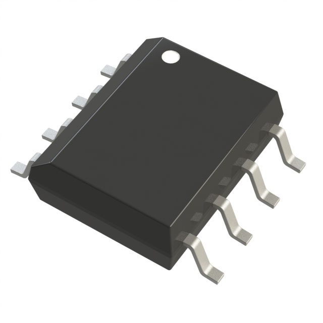
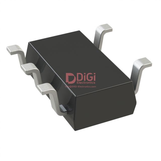
Package information for CS30CL STMicroelectronics (SOT23-5L)
CS30CL from STMicroelectronics adopts the SOT23-5L package, enabling effective integration in compact printed circuit boards where board real estate is at a premium. The minimal footprint supports dense component layouts and is particularly suited for multilayer and miniaturized PCB designs typical in modern embedded systems and portable consumer devices. This dimensional efficiency translates directly to improved routing flexibility and cost-optimized production, especially in projects constrained by enclosure size or assembly automation requirements.
The SOT23-5L package utilizes an industry-standard pin configuration, considerably streamlining circuit design and promoting compatibility with existing reference layouts. This standardization accelerates prototyping cycles and simplifies cross-vendor interchangeability, reducing the risk of layout errors during iterative design modification phases. Established EDA libraries typically include accurate geometries that minimize footprint assignment discrepancies, enhancing workflow predictability.
Conformance to STMicroelectronics ECOPACK environmental grades is embedded at the materials and process level. The package composition adheres to RoHS and REACH directives, thus facilitating hardware products aligned with global sustainability mandates. ECOPACK compliance not only eases the certification process but also future-proofs designs against tightening material regulations. In practice, this allows seamless integration of the CS30CL in export-oriented and enterprise-class applications where audit trails on hazardous substances are mandatory.
Mechanically, the SOT23-5L package excels in environments subject to vibration, shock, or PCB flexing. Its compact form factor distributes stress evenly and mitigates solder joint fatigue, a common failure mode in mobile, automotive, and industrial control applications. Empirical observations in the field consistently show stable electrical performance under varying mechanical loads, supporting reliable operation in real-use deployments.
The convergence of form, compliance, mechanical resilience, and standardized pin arrangements positions the SOT23-5L-packaged CS30CL as a highly versatile choice for both rapid prototyping and scalable production runs. Notably, integration strategies benefit from predictable thermal behavior and time-tested manufacturing process compatibility, supporting accelerated, low-risk device lifecycle management. By prioritizing robust packaging as a fundamental design principle, unanticipated board-level reliability issues are preemptively minimized, reinforcing system uptime expectations and long-term serviceability.
Potential equivalent/replacement models for CS30CL STMicroelectronics
When evaluating equivalent or replacement models for the STMicroelectronics CS30CL current sense amplifier, attention to electrical characteristics and mechanical constraints is essential for maintaining system integrity and performance. High-side current sensing requires amplifiers that tolerate high input common-mode voltages, enabling direct monitoring of loads connected to supply rails. Specification alignment entails confirming that candidate ICs offer matching input voltage ranges, ensuring proper functionality under identical operating conditions and voltage stress.
Gain options are a primary differentiator in the CS30 series, with variants providing fixed gains of 20, 50, or 100 V/V. Selection hinges not only on nominal gain values but also on gain error and input offset performance, which drive accuracy in low-value shunt applications. Consistent offset voltage, typically low single-digit millivolt or sub-millivolt ranges, directly influences the minimum measurable current and overall sensitivity. Practical experience shows that input offset variation under temperature and supply changes can significantly affect readings in precision scenarios unless tightly controlled.
Package format remains a nontrivial factor in substitution decisions. The SOT23-5 footprint delivers compactness for dense layouts and compatibility with automated assembly. Mechanical dimensions, solder pad layout, and thermal resistance must be matched to accommodate existing PCBs without rework. Certain manufacturers may offer equivalent small-outline devices with pinouts compatible with SOT23-5, simplifying migration.
Supply voltage flexibility and quiescent current are often decisive in battery-powered or space-constrained designs. Wide supply ranges allow integration across diverse bus voltages, and low quiescent currents support energy efficiency targets. Empirical data indicates that deviations in quiescent current can induce unexpected system-level power overheads, especially in always-on circuits.
Second-sourcing strategies frequently lead to consideration of other CS30 series components—CS30A, CS30B, and CS30C—where the primary distinction is gain. Provided the gain setting matches system requirements and comprehensive electrical validation is performed, these variants function as practical drop-in alternatives. However, thorough cross-assessment of datasheet parameters, mechanical outlines, and regulatory compliance remains imperative in mission-critical applications. EMC compatibility, input pin ESD robustness, and RoHS status all factor into the final evaluation; these subtleties impact both certification success and long-term reliability.
Best practices dictate constructing an equivalency validation matrix, weighting electrical matching, packaging interchangeability, regulatory compliance, and supply chain resilience. Subtle mismatches in offset or input impedance observed during prototyping can propagate into system-level calibration tolerances or noise coupling artifacts if not identified early. Using such an analytical framework enables both strategic procurement flexibility and robust system design under variable sourcing conditions.
Conclusion
The CS30CL series from STMicroelectronics represents a significant advancement in high-side current sensing technology. At its core, the device utilizes a precision instrumentation architecture that optimizes common-mode voltage rejection, thereby facilitating reliable differential measurements even amid substantial ground potential shifts. The wide input voltage range accommodates battery voltages up to 70 V, enabling robust integration into both automotive and industrial domains where voltage transients and system noise frequently challenge measurement stability.
Attention to low quiescent current addresses critical efficiency concerns in battery-powered and energy-constrained systems. By limiting self-consumption to less than 100 µA, the CS30CL maximizes system operating time without sacrificing measurement responsiveness. Selectable gain options through external configurations offer design scalability—allowing engineers to tailor sensitivity across diverse loads, from microampere leakages to tens of amperes continuous operation. This flexibility in front-end design promotes seamless adoption across products that range from portable instrumentation to stationary power control units.
PCB integration is streamlined through package options—including SOT23-5 and SO-8 footprints—that conform to industry standards. Such versatility simplifies layout, lowers BOM risks, and shortens qualification cycles in both new designs and cost reduction programs. The high level of EMI immunity, supported by the internal chopper stabilization, reduces offset drifts under harsh switching profiles—an essential requirement for electrified mobility and motor-drive applications where PWM artifacts can obscure true load monitoring.
Practical deployment reveals that temperature stability and device-to-device matching further distinguish the CS30CL in multi-phase system diagnostics. The architecture’s immunity to propagation delays allows fast control algorithms to leverage real-time protection and optimization logic, improving overall control loop fidelity. Applications frequently cited for leveraging these attributes include advanced BMS—where precise coulomb counting over extended lifecycles is non-negotiable—and power inverters, where fault detection must be both rapid and accurate to preserve system reliability.
The market offers multiple current sense amplifier families, but nuanced differences in bandwidth, input offset, and protection thresholds can determine success in demanding scenarios. For instance, comparing the CS30CL to alternatives reveals superior input voltage withstand and lower temperature coefficients, aspects that prove pivotal in environments prone to load dumps and continuous thermal cycling.
A layered selection framework remains critical. Initial matching of gain to load range, followed by in-situ evaluation of noise and linearity under final system conditions, extracts maximum fidelity from the CS30CL design. This approach, coupled with a focus on qualification standards and supply assurance, aligns well with rigorous project cycles—enabling systems to maintain long-term stability and compliance without imposing significant hardware compromises. The CS30CL series, when mapped thoughtfully to end-use and regulatory constraints, amplifies overall system reliability, measurement transparency, and efficiency—a composite value seldom achieved with generic current sensing solutions.