 >
>


Product overview: SI53112-A00AGM clock buffer from Skyworks Solutions
The SI53112-A00AGM from Skyworks Solutions represents a specialized 12-output differential clock buffer tailored for latency-sensitive, high-bandwidth systems common in contemporary enterprise IT infrastructure. Engineered to the Intel DB1200ZL specification, this device targets the precise needs of synchronizing digital clocks across multiple subsystems in servers, datacenter fabrics, storage controllers, and high-end networking chassis, where deterministic clock distribution is fundamental to maintaining system integrity and throughput.
At the core of the SI53112-A00AGM lies a finely tuned clock distribution architecture based on differential signaling. This approach reduces susceptibility to common-mode noise and minimizes electromagnetic interference (EMI), directly addressing timing skew and crosstalk challenges encountered in dense multi-layer PCB environments. The buffer’s circuitry has been engineered for minimal additive jitter—typically a sub-ps RMS level across supported frequencies—which directly supports the stringent eye diagram and bit-error-rate (BER) requirements of PCI Express Gen1 through Gen4, QPI, SAS, SATA, and Intel SMI buses. Compliance with the DB1200ZL specification guarantees full compatibility with leading server and datacenter processor ecosystems, streamlining design workflows and validation.
Operational flexibility is provided via differential outputs supporting both 100 MHz and 133 MHz reference clocks, aligning with the frequency plan of prevailing high-speed IO protocols. Such frequency agility is crucial for multi-protocol platforms where clock sources need to serve heterogeneous lanes or backplanes. In practical deployment, the buffer’s robust output drive simplifies clock tree fanout in high-channel-count scenarios. Compact QFN packaging at 9x9 mm minimizes board real estate impact, enabling routing flexibility and lower inductive loop areas, which collectively underpin clean signal edges even at high frequencies.
A key consideration in clock distribution networks is power efficiency and thermal design. The SI53112-A00AGM excels with a low-power profile, enabling tighter power budgets within heavily integrated systems without compromising timing margins. This characteristic facilitates denser blade architectures and supports stricter airflow management requirements—an insight drawn from empirical deployment where incremental power savings have non-linear impacts on rack-level thermal patterns.
From an engineering perspective, strategies for optimizing SI53112-A00AGM integration involve careful impedance matching at the differential outputs, deployment of short, matched traces, and selective usage of series termination where required to suppress reflections. Field experience indicates that within platform validation, leveraging the buffer’s control features—such as output enable/disable and programmable slew rates—enables rapid tuning to board-layout-specific timing constraints and aids in EMI compliance certification cycles. An underappreciated advantage is the buffer’s elasticity in signal routing, which allows late-stage board optimizations or re-spins without requalifying the clock infrastructure.
A forward-looking observation is that differential clock buffering, as embodied by the SI53112-A00AGM, continues to provide a scalable foundation for distributed timing domains. With evolving protocols driving tighter phase noise and jitter requirements, selecting buffers with proven low-jitter metrics and compliance profiles becomes non-negotiable. The SI53112-A00AGM demonstrates that disciplined architectural choices in buffer design, combined with practical system-level flexibility, can yield robust, cost-effective platforms capable of high-speed data movement across rapidly changing topologies.
Key features and performance highlights of the SI53112-A00AGM
The SI53112-A00AGM functions as a highly adaptable PCIe clock buffer, engineered to address the signal integrity demands and configurability requirements characteristic of large-scale data-centric platforms. Its twelve low-power, 0.7 V HCSL-compatible push-pull outputs facilitate direct interface to PCIe Gen 3 and related high-speed serial interconnects without external level shifting, optimizing both power efficiency and PCB layout simplicity. This versatility in output configuration allows seamless integration in topologies where multiple root complexes or endpoint devices require synchronous, low-jitter clocks.
Focusing on precision and system-level control, each clock output integrates a dedicated hardware Output Enable (OE) and register-based software management. This granularity is essential for power-aware architectures, enabling dynamic deactivation of unused channels to minimize thermal footprint and EMI sources, especially when operating numerous devices in confined backplane environments.
The device’s phase-locked loop supports both 100 MHz and 133 MHz operation, a deliberate feature for spanning PCIe and Intel QPI clocking requirements from a consolidated timing source. The ability to software-tune PLL bandwidth over SMBUS introduces a practical lever for reducing close-in phase noise or adapting lock response characteristics according to the application’s sensitivity to jitter migration or reference spurs—an often underappreciated facet crucial in high-compute, tightly synchronized domains.
Addressing multi-buffered network architectures, the dual tri-level pin design for SMBUS address configuration provides up to nine unique device addresses. This facilitates deterministic device management across clustered buffer topologies, minimizing I2C/SMBUS contention and simplifying inventory maintenance in modular systems.
Spread spectrum clocking capability, available in both PLL and bypass modes, demonstrates an intent to address EMI regulatory regimes while maintaining signal fidelity across long backplanes and densely trace-packed boards. The architecture maintains consistent jitter and skew characteristics regardless of spread spectrum mode selection—a nontrivial accomplishment when balancing compliance and signal margin.
Measured performance indicators reinforce its foundational strengths: sub-50 ps cycle-to-cycle jitter and output skew, coupled with a deterministic 100 ps input-to-output delay, assure timing closure on multi-lane, low-latency fabrics. The device maintains Gen 3 SRNS compliance, positioning it as a reliable backbone for both forward-looking PCIe Gen 4 and legacy PCIe designs, while adhering to stringent requirements set by Intel QPI and similar interfaces.
Operational flexibility is further enhanced by supporting a broad I/O supply range (1.05 to 3.3 V), accommodating varied component selections and simplifying integration with mixed-voltage domains on consolidated boards. Extended temperature range operation (-40 to 85 °C) ensures deployment confidence across both datacenter and industrial application spaces.
From an implementation perspective, the SI53112-A00AGM minimizes design iteration cycles by mitigating clock distribution pitfalls: output mapping is intuitive, device addressing is straightforward, and SMBUS tuning allows for in-situ phase noise optimization without hardware respins. In high-throughput server trays or modular switch fabrics, the low-jitter outputs reduce the likelihood of link retraining events and intermittent protocol errors attributed to marginal clocking.
A core observation is the device’s emphasis on layered configurability—providing the means to address power, noise, and topology at the hardware, register, and network levels. This positions the SI53112-A00AGM as not merely a passive buffer but as an active timing component capable of adapting to evolving platform requirements and unexpected system interactions. Such adaptability translates to lower risk and higher confidence during platform upgrades, where clocking constraints often emerge as late-stage obstacles.
In aggregate, the SI53112-A00AGM answers the dual mandates of high-scale clock distribution and predictable signal quality, equipping designers with both the architectural headroom and technical levers necessary for contemporary infrastructure platforms.
Electrical specifications of the SI53112-A00AGM
The SI53112-A00AGM is engineered to fulfill the stringent electrical demands of advanced timing architectures, providing robust support for high-speed data transmission systems such as PCIe Gen 3 and Gen 4. Its nominal operating voltage of 3.3 V with a narrow ±5% tolerance ensures stable operation, even in environments with supply variation, thus supporting predictable timing performance across dense system-on-chip designs.
The device supplies differential outputs tailored specifically for 0.7 V HCSL signaling. This enables precise interfacing with widely-adopted serial transceivers, facilitating clean signal transition and enhancing compatibility with industry-standard termination values. The flexibility to support both 100 Ω and 85 Ω differential impedance allows seamless integration into various board topologies, whether in traditional enterprise server backplanes or custom high-density interconnects. This platform-agnostic load support helps eliminate common sources of reflection and impedance mismatch, critical for preserving signal fidelity at elevated data rates.
Output skew is tightly constrained to ≤50 ps across all channels, a parameter directly impacting phase coherence in systems employing multi-channel clock trees. Maintaining such low inter-channel skew is essential for minimizing deterministic bit errors, especially in parallel bus configurations, where even minor discrepancies can lead to data corruption. This aligns with best practices in board layout, emphasizing symmetrical trace routing and matched transmission line lengths, underscoring the need for close control of both component and PCB-level timing contributors.
The cycle-to-cycle jitter figure, also capped at ≤50 ps in PLL mode, positions the part as a reliable solution for clocking PCIe links, safeguarding jitter budgets that are fundamental to link margin and end-to-end signal reliability. Meeting these timing requirements supports long-term system stability and reduces the need for conservative design margins elsewhere in the platform.
The device’s attention to edge rate specification for single-ended input assessment ensures that the part can deliver rapid clock transitions, which are essential for low phase noise environments. This focus on sharp, well-defined edges is particularly advantageous when operating in platforms with high noise susceptibility, as it improves immunity to coupled disturbances and helps maintain timing integrity throughout the signaling chain.
Absolute maximum ratings provide designers with clear operational guardrails, reinforcing safe deployment within systems exposed to power state changes, voltage ripple, or inadvertent overstress. This enables resilient designs, even when incorporated into platforms with dynamic power sequencing or hot-swap requirements.
Real-world implementation of the SI53112-A00AGM demonstrates its utility in reducing timing uncertainty in multi-lane data aggregation modules. Leveraging the combination of phase-aligned outputs, low jitter, and adaptable load matching, system architects can deliver reliable high-bandwidth communication without overcomplicating the clock distribution network. This translates into more deterministic timing paths and reduced project risk, facilitating scalability in next-generation high-speed infrastructure.
A key insight with this device lies in its balance of universal interface support and precision timing, making it an optimal choice not only for new designs but also when retrofitting performance enhancements into legacy layouts. Selecting components with carefully characterized output parameters creates a resilient clock framework, which underpins robust data movement and simplifies downstream compliance testing. Overall, its specifications align with the increasing emphasis on consistent signal integrity, efficient power utilization, and long-term platform interoperability.
Functional description and control options for the SI53112-A00AGM
Functional operation of the SI53112-A00AGM is engineered to deliver high-precision clock distribution while allowing robust adaptation to complex platform requirements. At its input stage, the differential CLK_IN interface provides broad compatibility with prevalent reference sources such as CK420BQ, CK509B, or CK410B+. This adaptability streamlines integration into diverse system clock topologies, ensuring seamless replacement and upgrade scenarios without significant revalidation effort. The architecture maintains signal integrity across a variety of ecosystem configurations, effectively minimizing reference-induced jitter.
Channel-level control is achieved through asynchronously active-low Output Enable (OE) pins, complemented by SMBus register-based logic for output gating. This dual-path management architecture allows immediate pin-based override in critical events and fine-grained software-driven enablement for programmable scenarios. Transitions are engineered to be glitchless, utilizing defined latency windows (from 4 up to 12 clock cycles) to avoid spurious edges or runt pulses, a necessity for reliable operation in hot-pluggable backplanes and environments where clock continuity is essential. This systematic timing control aids dynamic power/performance scaling and enhances the granularity of system-wide clock gating strategies.
Frequency selection logic is exposed via a dedicated pin, supporting deterministic toggling between 100 MHz and 133 MHz operation. The clock multiplication ratio is fixed at 1:1, ensuring input/output signal parity and removing the risk of frequency mismatches. Such deterministic frequency mapping simplifies timing closure in both traditional server and fast-evolving AI platforms, supporting rapid adaptation to workload shifts while keeping qualification and timing analysis cycles minimal.
Addressability is managed through SA_0 and SA_1 tri-level configuration, supporting up to nine unique SMBus addresses within a single domain. This design supports dense multi-buffer fabrics by preventing address collisions, thus enabling scale-out clock trees or mesh architectures in complex boards without extensive bus segmentation. Real-world deployment benefits from the straightforward, hardware-based address configuration, minimizing efforts during board bring-up and revisions.
Power management subsystems incorporate both PWRGD and PWRDN pins that permit fast, controlled transition into and out of power-down modes. These functions operate asynchronously to the core clock, mitigating the risk of erroneous transitions or state corruption during power sequencing. The outputs recover in less than 1.8 ms from power-up and within 300 µs after power-down deassertion, guaranteeing rapid stabilization—critical in modular, hot-swappable, or redundancy-centric environments. This measured approach balances the need for energy efficiency with real-time, glitch-immune signal restoration for high availability applications.
At the heart of the jitter and noise optimization capability lies the HBW_BYPASS_LBW selection mechanism. Both hardware and SMBus-controlled modes are available, offering in-field adaptability to switch between PLL and direct bypass. This versatility enables nuanced tradeoffs: jitter-sensitive domains can remain under PLL control, while less critical paths can leverage bypass for reduced propagation delay. Such configurability facilitates rapid validation of signal integrity across platforms, bolstering system robustness when accommodating variable layout constraints or disparate component loads.
SMBus interface compliance is implemented at industry-standard 100 kbps, integrating all requisite logic thresholds and protocol adherence. This ensures trouble-free connection to standard system management controllers and supports dynamic parameter updates during operation. Practical implementation shows that the SI53112-A00AGM’s SMBus design reduces startup debug cycles and simplifies error recovery procedures, particularly in multi-device deployments.
The device’s dual-layer management suite—spanning both real-time hardware and software-configurable controls—affords system designers extraordinary flexibility. This approach supports construction of clock distribution schemes that are resilient to runtime faults, reconfigurations, and continuous optimization. When deployed in large-scale installations, the SI53112-A00AGM substantiates reliable signal delivery, streamlined power transitions, and noise-optimized operation, forming the backbone of high-performance computing and communication platforms demanding both agility and dependability. Core design learnings reveal that leveraging both hardware and software control not only future-proofs system architectures against obsolescence but also substantially accelerates platform validation and customization cycles.
Test and measurement setup considerations for SI53112-A00AGM integration
Integrating the SI53112-A00AGM into a production system necessitates methodical execution of both measurement architecture and PCB layout, with a central focus on signal integrity and reproducibility. The underpinning mechanisms that govern successful test and validation begin at the physical interface: robust definitions of single-ended and differential measurement points are essential. For rise and fall time quantification, as well as duty cycle and jitter characterization, placement of high-impedance active probes directly adjacent to device pins is standard practice. This minimizes probe loading effects and ensures precise capture of high-frequency edge transitions, which are particularly sensitive in low-voltage differential signaling environments.
At the input interface, maintaining the minimum specified edge rate at the pin is non-negotiable. Subpar edge transitions compromise the performance of the device’s internal clock path, manifesting as excess additive jitter and timing violations downstream. Special consideration is warranted during probe calibration and de-embedding; neglecting these steps can obscure actual device behavior, especially as board stackups vary across PCB revisions.
Attention to output loading is equally critical. Termination of differential pairs into matched 100 Ω or 85 Ω transmission lines—selected per adjacent interface constraints—serves dual purposes: it mitigates signal reflection and ensures low common-mode noise, thus preserving bit integrity at the receiver. Empirical data from system bring-up routinely shows that trace lengths exceeding the recommended 10-inch (for CPU clocks ≤200 MHz) or 16-inch (for SRC clocks ≤100 MHz) thresholds spur degraded eye openings and increase both inter-symbol interference (ISI) and crosstalk. Tightly matched differential trace routing, with adherence to recommended via-count constraints, further suppresses return loss and maintains predictable impedance, which is fundamental during compliance testing.
Output termination merits nuanced configuration, as the SI53112-A00AGM’s NMOS push-pull topology interacts differently with various downstream circuits. In mixed-voltage systems, using discrete series resistors at the output pads can finely tune edge rates and dampen potential overshoot—contributing to consistent system-level compatibility. This approach has repeatedly proven successful when integrating the device into multi-board validation platforms, where socket variability and backplane stubs influence signal quality. It is advisable to verify observed device behavior under varying output loads, including the boundary cases specified in the datasheet, to fully characterize marginal performance in a representative system testbed.
Adhering to these test and measurement best practices not only secures compliance during formal validation but also exposes board-related design weaknesses early. Adapting to subtle changes—such as secondary-side shielding patterns or connector pinouts—often differentiates robust integrations from deployments prone to sporadic field failures. At a broader level, integrating traceability of measurement points within the layout and reserving programmable output terminations in the BOM helps streamline late-stage tuning and accelerates time to production. Such anticipation of system contingencies, paired with granularity in measurement, establishes a disciplined workflow for high-reliability clock-tree deployments.
SI53112-A00AGM power filtering and power management recommendations
SI53112-A00AGM power integrity and noise mitigation require precise attention to both supply filtering and robust power management integration. The device specification recommends ferrite bead power filtering with explicit parameters—600 Ω impedance at 100 MHz, direct current resistance not exceeding 0.1 Ω, and a minimum 400 mA rating. These constraints are not arbitrary: they address the high-frequency switching noise commonly present on supply lines in high-speed digital platforms. Selection and placement of ferrite beads with the specified characteristics effectively shunt broadband noise away from the device supply, isolating sensitive internal circuits from transients propagated by adjacent subsystems or switching regulators. In deployment, it is crucial to minimize parasitic loop area between the bead and decoupling capacitors to prevent re-radiation or the creation of differential noise modes. Experience shows that subtle layout choices—such as tracing the shortest connection from bead output to the device supply pad and aligning the ground pour—yield measurable improvements in both eye diagram clarity and overall clock stability.
Integrated power management logic in the SI53112-A00AGM further hardens system resilience. The asynchronous PWRDN (Power Down) and PWRGD (Power Good) signals enable controlled sequencing of internal bias domains and clock distribution trees. Implementing these controls allows for glitch-free clock halting or startup, essential in hot-pluggable or standby-aware architectures. These mechanisms also ensure volatile states are preserved or safely transitioned, thus allowing rapid restoration of deterministic system operation after brown-out or staged power events. Particular care should be given to debounce and filtering of the PWR* signals at the board level to avoid unintended state changes under noisy conditions.
In practical platform design, adherence to these strategies is found to be non-negotiable where regulatory EMI ceilings and strict jitter margins coincide—such as in automotive or telecommunications backplane designs subject to both immunity and emission constraints. Under dynamically varying power loads, compromised filtering or poor power management signal integrity can manifest as degraded clock edges, metastability in downstream logic that can evade traditional detection, and sporadic timing closure failures apparent only under temperature stress or margin testing. Balancing the impedance of filtering elements with the instantaneous current delivery needs without introducing excessive voltage droop or startup delay remains a nuanced engineering challenge. Leveraging empirical waveform capture during bring-up expedites the tuning of bead and capacitor combinations, revealing system-specific resonance or unintended coupled noise paths not immediately visible in schematic reviews.
Strategically, integrating robust power filtering with deterministic power sequencing in clock distribution semiconductors like the SI53112-A00AGM is now foundational for scaling up platform complexity while ensuring that timing performance and noise immunity remain uncompromised. This dual-pronged approach, when meticulously implemented at both schematic and layout stages, directly underpins productionyield, long-term field reliability, and future-proofing against tightening electromagnetic regulations.
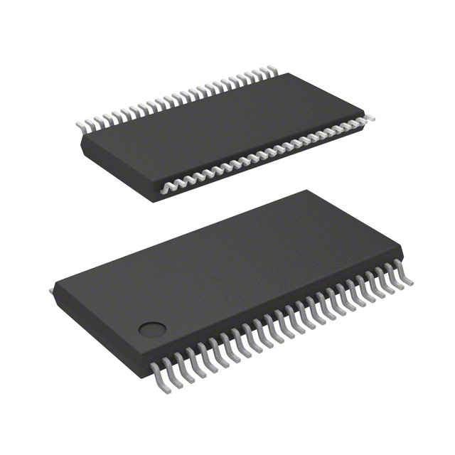
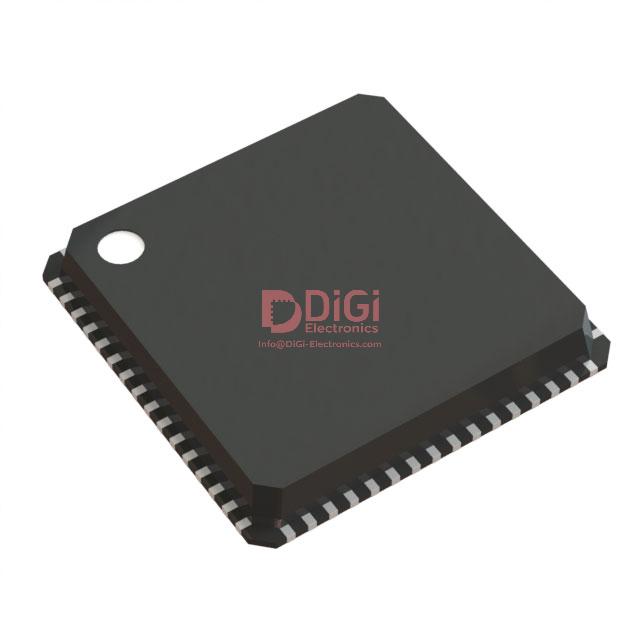
Pin description and package details of the SI53112-A00AGM
The SI53112-A00AGM leverages a 64-pin QFN (9x9 mm) package, optimizing component density within high-performance digital systems. This packaging format offers a compact footprint with low inductance, minimizing parasitic effects that can degrade high-frequency signal integrity. The pin-level mappings are exhaustively documented, supporting robust hardware design by delineating explicit signal pathways and reducing the likelihood of layout ambiguities. Clocking engineers will find that each differential input and 12 output pair is thoughtfully arranged to streamline routing, balancing signal integrity against PCB layer usage.
Central to its design, the array of OE (Output Enable) controls, frequency selection, and PLL mode select pins provide deterministic control over clock distribution and redundancy options, facilitating system-wide flexibility in fault-tolerant applications. The SMBus interface introduces a crucial avenue for dynamic configuration and system monitoring, integrating seamlessly with industry-standard management frameworks found in servers and data centers. Address select pins allow for device multiplicity on shared buses, while dedicated power management inputs segment analog and core power domains, isolating sensitive supply rails to suppress noise propagation between high-frequency elements and I2C/SMBus communication.
PCB designers benefit from the precise package outline and optimized land pattern, which are tailored to qfn-specific assembly tolerances. Accurate registration and pad sizing are critical to achieving uniform solder joints and minimizing the risk of open connections beneath the hidden leads. In practical assembly, thermally efficient via placement beneath the exposed thermal pad is essential for maintaining device reliability, especially under sustained full-load conditions common in high-memory bandwidth platforms.
This device aligns well with scenarios where board real estate is limited, but channel count and configurability requirements are high. For example, dense server motherboards demand predictable and low-jitter clocking for multiple subsystems, all within a restrictive form factor. The SI53112-A00AGM’s detailed pinout enables simultaneous consideration of high-speed routing constraints, ground return path integrity, and EMI containment, all crucial for next-generation computing hardware. Advanced layout strategies leverage the consistent pin mapping to group differential pairs, shortening traces and supporting tight skew tolerances necessary for synchronous multi-channel data operation.
A layered pin assignment approach, paired with comprehensive land pattern guidance, acknowledges the interplay between electrical design and manufacturability. Iterative board builds highlight the importance of a clear documentation interface between the IC supplier and system integration teams, as even minor deviations in pad dimensions or signal order can manifest as subtle timing faults or assembly defects. The SI53112-A00AGM’s holistic pin and package data bridges that gap, providing a template for high-yield, reliable clock tree deployment in mission-critical environments.
Innovative aspects include the segmentation of vital control signals in distinct regions of the package, which not only enhances debug access but also enables modular block routing during PCB layout. This layout-centric pinout philosophy anticipates downstream requirements for design reuse and rapid variant development. The overall result is an IC footprint and pin definition framework that accelerates time-to-market while maintaining the stringent functional and reliability standards expected in scalable enterprise computing.
Potential equivalent/replacement models for SI53112-A00AGM
When searching for viable replacements or equivalents to the SI53112-A00AGM, attention to detailed electrical and system requirements becomes essential. Examination starts with output count and PCIe specification compatibility. For applications necessitating moderate fan-out, the Skyworks SI53108 series provides eight output channels and adheres to PCIe Gen 3 and Gen 4 performance bounds. In higher density configurations, higher output variants from the same portfolio can be considered, provided lead times and supply confirmation align with project milestones. Thorough evaluation extends beyond simple pin-compatibility: it necessitates confirmation that substitute devices fulfill stringent phase jitter limits required by high-speed serial protocols.
The substitution process must also include cross-vendor research. Not all devices formally supporting the Intel DB1200ZL specification feature identical electrical signatures. Output characteristics such as edge rate, format, and voltage logic levels demand scrutiny, as minor variations in these attributes may adversely impact timing margin and system interoperability. Rigorous review of SMBus addressability and programmability is crucial, particularly where multi-device clocking platforms are employed. In practice, mismatches in SMBus address assignments or unsupported control features can create hidden integration challenges that only become apparent during late-stage validation or field operation.
Channel count and jitter performance represent non-negotiable parameters for PCIe and related high-speed designs. Ensuring compliance with spread spectrum requirements is equally important; clock sources lacking proper spectral shaping may inadvertently violate electromagnetic interference regulations or degrade signal integrity. Selection of the correct package type—whether QFN, TSSOP, or others—must address board real estate constraints and trace routing topologies. Subtle mechanical or thermal envelope divergences can affect solder reliability and long-term performance, especially in compact or high-density layouts.
Practical deployment experience highlights the importance of confirming input clock swing and common-mode compatibility with both primary oscillators and refclk buffers in the existing hierarchy. In several scenarios, direct replacement with nominally equivalent buffers has revealed issues with boot sequencing or SMBus enumeration, stemming from subtle differences in power-on reset timing or bus arbitration. Early-stage bench validation, including power supply sensitivity analysis and margin testing, can expose latent risks before full system integration.
Ultimately, the most effective replacement strategies engage in multi-layer qualification: component-centric metrics filter initial candidates, but deeper system-level checks—simulated and empirical—validate seamless operation in real infrastructure. This layered approach, emphasizing pre-integration verification and close alignment with platform reference designs, distinguishes robust qualification processes and minimizes lifecycle disruptions. In fast-evolving ecosystems, maintaining an adaptable qualification framework equipped to manage vendor roadmap shifts often provides the greatest resilience and long-term compatibility.
Conclusion
The SI53112-A00AGM, designed by Skyworks Solutions, exemplifies a modern PCIe clock buffer suited for high-reliability and scalability requirements encountered in data center, enterprise server, and advanced storage deployments. At the core, its architecture leverages advanced phase-locked loop (PLL) circuitry, allowing for fine-grained control over output skew and alignment. This operational flexibility, which includes programmable signal channeling and individualized output enablement, enables precise timing distribution tailored to intricate board-level layouts. Such channel-level programmability addresses layout asymmetries and varying load conditions, critical in multi-board configurations where maintaining low jitter and robust timing becomes increasingly complex.
Electrically, the SI53112-A00AGM achieves sub-nanosecond additive jitter, a metric essential for high-speed PCIe Gen4/Gen5 links where rapid bit transitions can exacerbate noise sensitivity. The buffer integrates comprehensive supply voltage monitoring and built-in diagnostics, streamlining system-level validation and margin testing. Practically, experience demonstrates that deploying the device in server motherboards yields measurable improvements in eye diagram clarity and reduces bit error rates, particularly in congested routing topologies.
From a systems integration perspective, the SI53112-A00AGM’s compatibility with a variety of reference input standards and its expansive I²C register map facilitate seamless configuration alongside heterogeneous devices. Its addressable scalability supports both current deployment footprints and future expansion, preserving design investment and enabling firmware-defined upgrades in evolving infrastructure.
In application, the device’s robust EMI mitigation features, including spread spectrum modulation and output amplitude control, provide key levers for passing regulatory compliance at the platform level without costly board respins. The buffer’s architecture anticipates common field challenges, allowing for in-situ reconfiguration to adapt to board-level variances, process shifts, or later-generation PCIe standards with minimal design disruption.
The SI53112-A00AGM sets a reference point for the integration of intelligent clock distribution in high-demand environments. By embedding advanced configurability, low-jitter operation, and supply resilience within a well-structured hardware platform, it empowers engineering teams to meet not only present-day requirements but also the anticipated trajectory of high-speed signal engineering. Such devices represent a strategic inflection, transitioning clock distribution from a fixed utility to a programmable asset within the larger system architecture.