>
>


Product Overview: Sharp PC925L0NIP0F Series
The Sharp PC925L0NIP0F represents a disciplined approach to the optical isolation of gate driving signals in demanding power conversion environments. At its core, the PC925L0NIP0F employs optocoupler technology to ensure galvanic isolation, utilizing a high-efficiency LED-photodetector pair to transmit gate drive commands while maintaining a reinforced safety barrier. This device sustains a rated isolation voltage of 5,000 Vrms, safeguarding control logic from high-voltage transients and ground potential differences that frequently occur in inverter topologies and industrial drives. Such robust isolation ensures both compliance with international safety standards and persistent reliability in electrically noisy environments.
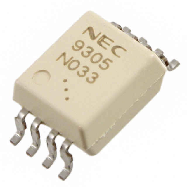
The device’s 8-pin, gullwing surface-mount package facilitates straightforward integration into high-density PCBs, particularly in applications where board real estate is at a premium. The construction includes an optimized signal transfer path with minimized internal propagation delay, aligning with the need for tight timing control in high-frequency switching scenarios. With a peak output current of 2.5A, the PC925L0NIP0F effectively drives large gate charge IGBT and MOSFET components, supporting fast switching edges and minimizing on-state losses. For multi-phase inverters or systems demanding parallel gate drives, the device demonstrates consistent performance batch-to-batch, reducing the need for extensive post-fabrication tuning.
Electromagnetic immunity is engineered through internal shielding and circuit design choices that reject common mode noise, an essential requirement when the device is exposed to dV/dt events from high-side switches or parasitic coupling within complex power modules. The input’s CMOS/TTL compatibility streamlines connection to modern microcontrollers or DSPs without level-shifting circuitry, ensuring unambiguous triggering even under fast transient load steps. Implementers have observed that the PC925L0NIP0F’s noise margin and common mode transient immunity are typically sufficient to eliminate false triggering even in transformerless or ground-referenced architectures.
From a practical standpoint, deployment in multilevel inverter bridges and precision motor drives has revealed the value of consistent isolation parameters over the operating temperature range; thermal drift is marginal, enabling predictable delay matching and reducing system-level compensation overhead. The gullwing package’s mechanical resilience also improves manufacturability, with automated pick-and-place yielding consistently high joint integrity after reflow. System architects benefit from the device’s straightforward thermal modeling due to its low power dissipation and well-characterized switching losses.
One unique observation regarding obsolescence of the PC925L0NIP0F is the subsequent migration path to digital-isolated or capacitive-coupled drivers. While such newer devices extend bandwidth and further miniaturize isolation, the legacy PC925L0NIP0F offers a balanced trade-off between noise immunity, simplicity, and proven reliability—a consideration that remains pivotal in retrofit or long-service-life applications where qualification risks and system redesign costs must be tightly controlled. This underlines the importance of platform stability in cost-sensitive or safety-critical domains.
Key Features and Technology of the Sharp PC925L0NIP0F
The Sharp PC925L0NIP0F is purpose-built for fast-switching power electronics, with a feature set engineered to address the demanding isolation and control requirements intrinsic to gate driver and power conversion circuits. At its core, this device utilizes an integrated OPIC (Optical IC) architecture, wherein a light-detecting photodiode is monolithically combined with analog and digital signal-processing circuitry. This configuration enables intrinsic galvanic isolation, realized through optical coupling. By eliminating direct electrical pathways, the OPIC solution provides robust immunity against ground potential differences and high common-mode noise, a critical aspect for reliable operation in high-voltage systems.
The device’s 5,000 Vrms isolation rating between input and output directly supports safe operation in industrial inverters, motor drives, and solar string inverters, where isolation barriers must withstand transients far above rated line voltages. The minimum ±15 kV/μs common-mode transient immunity endows the PC925L0NIP0F with resilience against high dV/dt events, such as those generated by fast IGBT or SiC MOSFET switching edges. This characteristic is especially valuable where poor CMTI could otherwise result in erroneous gate drive, system malfunction, or excessive EMI propagation.
A supply voltage range of 15V to 30V ensures flexibility during design-in phases, supporting conventional ±15V as well as modern 20V and 24V drive schemes. The output stage's typical continuous current capability of 2.0A (source and sink) with a 2.5A peak margin is tailored for charging and discharging the capacitive gates of modern power MOSFETs or IGBTs, ensuring clean and decisive turn-on and turn-off transitions even with large devices. Fast output rise and fall times, each typically 100 ns, facilitate high-frequency switching with minimal delay and enhance overall system efficiency by reducing total switching losses.
By minimizing pulse width distortion, the device maintains tight timing accuracy between control and load—a prerequisite for achieving symmetric dead-time control in half-bridge and full-bridge converter topologies. This allows for higher fidelity in pulse-width modulation (PWM) schemes, directly translating into reduced distortion and improved power stage efficiency. Real-world implementation highlights the importance of such temporal precision: even small variations in signal timing, if left unaddressed, can lead to increased heat dissipation and lower system reliability.
Mechanically, the double-molded package structure reinforces the device’s electrical isolation through robust creepage and clearance distances, vital for enduring high-voltage surges and mechanical stress during PCB manufacturing and deployment. Compliance with RoHS directives and a lead-free finish ensures compatibility with contemporary environmental standards and the demands of automated assembly processes, minimizing reflow soldering anomalies and promoting uniform quality across production batches.
A distinctive aspect of the PC925L0NIP0F is its blend of legacy reliability with future-ready electrical performance. Unlike conventional optocouplers, which often face bandwidth and aging-related degradation, the integrated signal-processing approach of OPIC technology facilitates higher speed and prolonged signal integrity with reduced drift over operational life. This makes the component advantageous for both upgrade initiatives in legacy systems and the development of advanced, high-density power platforms. In practice, field deployments confirm that selecting a gate driver with superior CMTI and switching characteristics yields tangible benefits in reducing noise propagation and ensuring deterministic control, particularly in electrically harsh industrial environments.
Within the broader perspective of system reliability and efficiency, such feature integration reinforces the trend toward highly integrated, optically isolated driver solutions as a mainstay for next-generation power conversion architectures.
Internal Structure and Functional Block Diagram of the Sharp PC925L0NIP0F
The internal architecture of the Sharp PC925L0NIP0F is engineered for optimal isolation and signal fidelity within gate drive applications. At the core, the infrared emitting diode initiates optical signal transmission, forming the primary interface for galvanic isolation. The diode’s emission is precisely aligned to activate the OPIC output IC, which leverages isolation barriers and custom amplifier chains to convert weak optical input into high-fidelity, logic-level outputs. This layered approach permits gate drive signals to traverse high-voltage boundaries without risk of electrical coupling, ensuring robust operation even amidst transient disturbances.
The OPIC block integrates multi-stage amplifiers with direct-drive logic, tailored for the fast switching requirements of power MOSFETs and IGBTs. These stages employ high slew-rate devices and transient rejection circuits, reducing propagation delay and suppressing spurious output states. This internal configuration maintains strict temporal correlation between input LED activation and output logic transitions, supporting consistent turn-on and turn-off waveforms in pulse-width modulated power electronics.
An 8-pin SMT gullwing package encapsulates the device, optimizing pad layout for low-inductance connections and thermal dissipation. The input pins accommodate the LED’s current drive profile, with carefully controlled impedance paths minimizing input voltage overshoots. Output assignments include isolated supply, ground, and logic signals, facilitating straightforward routing in multilayer PCBs. This arrangement directly contributes to reduced cross-talk and enhanced immunity against radiated emissions—a necessity for inverter gate drivers deployed in demanding electromagnetic environments.
Integrating optical detection and digital output stages onto a single IC yields considerable engineering benefits. Signal integrity is preserved across the isolation barrier, with noise rejection upholding operational reliability. Practical deployment highlights the device’s capability to withstand common-mode voltage swings without false triggering, an attribute observed in high-power inverter designs subject to substantial switching transients. The combination of optical isolation and fast amplifier logic enables precise control of power switches, while also streamlining design iterations by reducing external component counts.
A notable insight arises from the balance of internal delay and noise suppression: the PC925L0NIP0F achieves high-speed switching performance without sacrificing drive consistency. This dual optimization is fundamental for maintaining efficiency and safety in inverter circuits operating at elevated frequencies. By embedding amplification and signal conditioning within the OPIC, the device positions itself as a plug-and-play solution for engineers seeking reliability, isolation, and operational margin in modern power conversion layouts.
Electrical Characteristics and Performance of the Sharp PC925L0NIP0F
The Sharp PC925L0NIP0F integrates a high-speed optically isolated gate driver within a compact SO-8 package, focusing on efficient signal transmission while maintaining stringent isolation and reliability standards. At its core, the PC925L0NIP0F utilizes an advanced opto-coupler structure, which ensures galvanic isolation between input and output circuits, safeguarding sensitive control logic from high-voltage transients. The isolation resistance greater than 5×10¹⁰ Ω at 500V DC provides robust protection against breakdown and crosstalk, critical for industrial drives and inverter applications.
A notable attribute lies in its precisely calibrated input and output parameters. The low typical input forward voltage of 1.2V at 20mA facilitates energy-efficient triggering from logic-level sources, while a tight input current threshold (IFLH max 10mA) enhances noise immunity and guards against inadvertent turn-ons even under adverse operating conditions. These characteristics ensure high predictability in switching, especially where input signal integrity is paramount, such as in programmable logic controllers and isolated microcontroller interfaces.
The wide supply voltage window (15V to 30V) enables compatibility with a range of power supply rails, supporting straightforward integration into both legacy and modern control systems. Output swing is significant, with the high-level output reaching a typical 22V and the low side remaining below 0.5V, enabling direct gate drive for high-side and low-side MOSFETs or IGBTs in switching topologies. This direct drive is further enhanced by the substantial output drive capability—2.0A average and up to 2.5A peak—allowing the device to rapidly charge and discharge gate capacitances, minimizing turn-on and turn-off delays in fast-switching power stages.
Propagation delay is another key strength. With a maximum of 2.0μs and typical performance well below this figure, the PC925L0NIP0F supports high-frequency PWM operation with minimal phase distortion and low skew between input and output edges. This attribute becomes particularly beneficial in precision motor control and high-efficiency power conversion, where consistent timing directly impacts system performance and EMI reduction efforts.
Thermal and leakage specifications contribute significantly to the device’s deployment in high-density layouts. The 550mW power dissipation ceiling, coupled with a maximum leakage below 500 nA, ensures stable operation under continuous switching without thermal run-away or signal integrity degradation—an essential consideration in tightly-packed power management boards or in applications where heat sinking options are constrained.
In practical deployment, reliable opto-isolated drivers like the PC925L0NIP0F demonstrate exceptional resilience against high common-mode transients, a recurring issue in motor drives and inverter bridges. Their low-distortion output permits feedback and protection circuits to maintain safe and efficient system behavior at high slew rates, while the tight input thresholds avoid false triggers in noisy environments.
The device’s lean switching characteristics, robust isolation barrier, and high output drive combine to streamline EMI compliance and reduce total BOM cost by eliminating the need for supplemental buffer or level-shifter components. This integrated approach not only simplifies PCB routing and increases the longevity of downstream devices but also enables the realization of compact, high-reliability power delivery subsystems.
A core insight is that devices engineered with such a balance of speed, isolation, and noise immunity offer a strategic advantage in applications where safety, timing precision, and energy efficiency intersect. By refining each specification parameter, the PC925L0NIP0F sets a reference point for next-generation optically-isolated driver solutions in demanding automotive, industrial, and renewable energy domains.
Mechanical Dimensions and Mounting Options for the Sharp PC925L0NIP0F
Mechanical dimensions and mounting options for the Sharp PC925L0NIP0F are optimized to address constraints commonly found in densely packed multi-layer PCB assemblies. The 8-pin surface-mount package, employing gullwing leads, affords precise placement and stable solder joint integrity during high-speed automated reflow processes. With a body footprint of 9.66 × 7.62 mm, the device achieves a balance between miniaturization and accessibility for inspection, minimizing shadowing effects for AOI (Automated Optical Inspection) systems. The height parameter, restricted to 3.5 mm, permits integration into low-profile enclosures and facilitates efficient airflow paths, reducing thermal accumulation in stacked board architectures.
Lead pitch at 2.54 mm conforms to standardized mounting grids, supporting straightforward trace routing and minimizing the risk of solder bridging during mass production. Experience shows that this spacing simplifies rework scenarios, as leads are accessible for fine-pitch soldering tools without excessive thermal stress. The SnCu plating, compliant with RoHS and other environmental directives, ensures solderability under lead-free conditions and resists whisker formation during extended field operation.
The mechanical envelope is not merely a passive constraint; it actively enables high-density designs in switch-mode power supplies, signal isolation interfaces, and industrial control modules. The package geometry, combined with robust gullwing lead structure, mitigates mechanical fatigue under vibrational loads and repeated thermal cycling, especially in equipment subjected to harsh deployment environments. Utilization of the PC925L0NIP0F in automated assembly lines reveals consistent coplanarity and solder joint reliability, even at reflow peak temperatures of 270°C for 10 seconds—a profile compatible with contemporary lead-free process windows. Integration is streamlined: component placement algorithms exploit the symmetrical lead layout to maximize PCB space utilization, while the package's planar stability supports precise paste deposition and minimal tombstoning risk.
A core viewpoint emerges from practical deployment: the dimensional choices of the PC925L0NIP0F are not solely dictated by electrical performance but are deeply interwoven with manufacturing yield and mechanical resilience. By anchoring design criteria in both electrical and assembly realities, the package serves broad application spaces—from consumer AV power modules to industrial signal isolation clusters—without demanding custom mounting adaptations or complex board redesigns. This synergy between mechanical engineering and surface-mount technology exemplifies a holistic approach to component specification, ensuring long-term reliability and production efficiency.
Safety, Agency Approvals, and Compliance: Sharp PC925L0NIP0F
The PC925L0NIP0F exemplifies high standards in optoelectronic isolation, with certification rigorously aligned to global regulatory frameworks. UL1577 certification provisions double isolation, critical in applications demanding robust protection against electrical shock or intersystem voltage transients. The documentation under File No. E64380, inherited from the PC924L Series, underpins traceability and ensures seamless integration into systems requiring third-party safety approvals.
DIN EN60747-5-2 compliance, as the VDE 0884 successor (File No. 40008898), strengthens acceptance in the European market, particularly for equipment slated for industrial automation, medical devices, and railway signaling. This standard evaluates the integrity of internal insulation and guarantees safe functional isolation, bolstering system reliability in scenarios where malfunction could trigger hazardous events.
The encapsulation achieves UL94V-0 flammability rating, elevating its suitability for layered safety architectures. Materials meeting this threshold halt flame propagation during overcurrent faults, enabling designs to fulfill stringent fire protection mandates—an essential requirement in high-density control panels or mission-critical embedded platforms.
Moisture Sensitivity Level 1 designation delivers operational resilience throughout the logistics chain. Devices with unlimited shelf life under ≤30°C/85%RH withstand lengthy storage and aggressive reflow soldering regimes without material degradation, ensuring consistent optoelectronic performance and eliminating risks associated with latent failures post-assembly.
RoHS compliance is integral in environmentally regulated markets, facilitating exports across jurisdictions with restrictive lead and hazardous material thresholds. This compliance supports manufacturers in maintaining supply chain sustainability and eases the passage of finished goods through conformity assessment audits.
From practical deployment, leveraging a component with comprehensive agency approvals streamlines end-system qualification, reducing development overhead from repeated test cycles and documentation. The assurance of established safety certifications, coupled with robust material properties and environmental resilience, enables designers to target mission-critical markets—where uptime, layered protection, and audit traceability form the core engineering requirements.
A unique insight is observed in the interplay between regulatory compliance and accelerated time-to-market. By minimizing certification friction and providing exhaustive documentation, the PC925L0NIP0F actively enables innovation cycles, particularly in sectors constrained by evolving safety and environmental regulations. This strategic alignment supports system architects in advancing modular and scalable platforms without compromising regulatory traction or operational integrity.
Real-World Applications and Design Considerations for the PC925L0NIP0F
The PC925L0NIP0F serves as an integrated optically-isolated gate driver, specifically optimized for high-side and low-side switching of IGBT and MOSFET power stages in demanding industrial contexts. Its implementation centers around environments with elevated switching voltages, significant common-mode transients, and stringent noise immunity requirements, such as vector-controlled motor drives, grid-tied inverter modules, and uninterruptible power supply architectures. In these domains, system integrity relies heavily on the device's ability to maintain robust isolation and precise signal transfer across a rapidly changing potential.
At the core, the device’s high common-mode transient immunity (CMTI) rating—typically exceeding 15 kV/μs—plays a decisive role in withstanding large dv/dt edges, common in inverter legs and fast-switching topologies. This prevents false turn-on or inadvertent gate triggering caused by capacitive coupling and ground bounce phenomena. During high-frequency operation, the opto-isolator structure minimizes propagation delay skew, ensuring symmetrical switching and reducing shoot-through risk in half-bridge implementations. Practical deployment in such scenarios has shown that this CMTI performance greatly reduces susceptibility to parasitic latch-up and signal corruption, supporting extended operational reliability.
Optimal PCB design is essential for leveraging the PC925L0NIP0F’s isolation capabilities. Adequate creepage and clearance distances—meeting or exceeding regulatory requirements such as UL1577 or IEC 60950—must be allocated between input and output domains, especially when switching above 600 V. Experience demonstrates that incorporating cutouts and slotting underneath the device footprint further mitigates surface tracking under contaminants or adverse humidity conditions.
Device longevity also hinges on strict input current derating, as sustained operation above the 25 mA absolute maximum can accelerate LED degradation within the isolation element. In field deployments, gate control circuits integrate series resistors or constant-current drivers to maintain steady input drive while accommodating logic-level fluctuations and power supply variation. For control interface flexibility, signal conditioning ensures compatibility with both 3.3 V and 5 V logic families. Integration of Schmitt-trigger buffers or level shifters at the front-end prevents erratic device behavior during slow input transitions, which is critical for fail-safe control.
Thermal management, though often underestimated in opto-coupled drivers, remains a foundational design concern. Dissipated power originates from both input-side forward voltage drop and output-stage switching losses, especially during rapid gate charge/discharge events with high-channel capacitance devices. Empirical circuit iterations reinforce that a combination of low thermal resistance package mounting, optimized gate resistors, and careful layout trace sizing maintains junction temperature within datasheet limits, even at elevated ambient temperatures. Failure to address these factors can manifest as frequency-dependent output degradation and, in severe cases, premature device failure.
Notably, although standard application notes focus on conventional circuit topologies, leveraging the PC925L0NIP0F in modular power electronics—such as plug-and-play inverter stacks or hybrid power unit architectures—reveals its utility in supporting scalable designs. The device’s robust noise rejection combined with straightforward logic-level interfacing simplifies rapid system integration, reducing time to market for industrial automation projects. In summary, disciplined adherence to layout, drive, and thermal guidelines is pivotal in translating the PC925L0NIP0F’s isolation and drive strengths to high-reliability field performance.
Potential Equivalent/Replacement Models for the Sharp PC925L0NIP0F Series
The decommissioning of the Sharp PC925L0NIP0F optocoupler series has accelerated the need for precise evaluation and selection of potential replacements. Replacement models must deliver equivalent or superior performance across key parameters including isolation voltage, drive strength, mechanical compatibility, and regulatory adherence. Within Sharp’s portfolio, the PC924L0NIP0F stands out as a near drop-in substitute, maintaining both the SMD gullwing package and matched electrical characteristics. This continuity preserves PCB layout integrity, minimizing redesign effort and mitigating supply chain disruptions during transition.
A layered approach to identifying cross-manufacturer alternatives necessitates a focus on the underlying mechanics of optical gate driver operation. Devices with isolation ratings at or above 5 kVrms, such as those from Vishay, Toshiba, or Renesas, provide robust separation between input and output stages, crucial for high-voltage systems. Selection criteria should prioritize gate drive capabilities of 2A or above, ensuring reliable activation of high-side MOSFETs or IGBTs under demanding conditions. Additionally, fast switching dynamics, typically characterized by rise and fall times no greater than 200 ns, are essential for minimizing propagation delays and mitigating switching losses in pulse-width modulation and inverter circuits.
Regulatory compliance forms a fundamental baseline for substitute qualification. Adherence to UL1577 and VDE0884 standards assures end-to-end insulation integrity, with rigorous testing for creepage and clearance distances. The growing adoption of reinforced isolation in industrial and automotive designs underscores the importance of multi-layered verification beyond datasheet review. Empirical qualification, through direct deployment in representative operating environments, enables exposure to transient disturbances and noise that may not manifest in controlled laboratory conditions. This practice exposes subtle incompatibilities—timing mismatches, susceptibility to electromagnetic interference, or thermal drift—which often dictate final selection.
Application-driven experience reveals that successful device substitution is rarely determined solely by nameplate specifications. Subtle differences in input threshold voltages or output drive profiles can impact circuit stability, particularly in high-frequency switching use cases. Painstaking attention to PCB grounding schemes and local decoupling is required to sustain performance parity when legacy devices are swapped. Recent trends show that optocoupler selection increasingly factors in lifetime reliability metrics and field failure rates, nudging procurement toward models with proven track records in similar architectures.
An implicit insight guiding this process is that adaptability and foresight in component selection yield maximum resilience against obsolescence. Engineers who prioritize not only immediate specification matching but also the supplier’s support roadmap and device longevity position their systems for extended serviceability and reduced maintenance overhead. Integration of these considerations into the qualification workflow enhances risk mitigation and strengthens product robustness throughout the lifecycle.
Conclusion
The Sharp PC925L0NIP0F series exemplifies sophisticated design principles in the field of isolated gate driving for high-voltage power electronics. Its architecture integrates an optically coupled isolation barrier, delivering high common-mode transient immunity and precise signal fidelity across the galvanic divide. This fundamental isolation mechanism remains instrumental when addressing both safety and electromagnetic interference (EMI) requirements in inverter systems and industrial motor drives. The PC925L0NIP0F achieves low propagation delay and tight pulse-width distortion, ensuring rapid and accurate switching events, which directly translate to higher system efficiency and reduced dynamic losses.
The reliability framework of this component rests on extensive safety certifications and rigorous insulation strength, supporting safe operation in environments subject to surges, noise, and high-voltage transients. The internal photodiode and high-gain amplifier are engineered to maintain consistent transfer characteristics over years of operation, minimizing gate charge timing jitter. This stability is non-trivial, especially for long-term deployments like photovoltaic inverters or critical process controllers, where partial discharge or insulation aging can compromise isolated signal integrity. Engineers faced with legacy equipment must be conscious of substitute choices, carefully validating creepage, clearance specifications, and temperature dependence, as sharp deviations can undermine system-level regulatory compliance.
Despite formal obsolescence, the specification benchmarks established by the PC925L0NIP0F endure as practical reference points for evaluating modern isolated drive solutions. Key features such as high CTR (current transfer ratio) linearity, input-output isolation voltage, and robust package molding standards inform comparative analysis when transitioning to wide bandgap semiconductor drivers or integrating feedback-rich circuits. Selection for retrofit or forward design must consider not only data sheet equivalence but also the nuanced interplay of switching behavior within actual converter topologies—for instance, gate drive overshoot mitigation and dv/dt resilience remain critical for SiC and GaN fast-switching applications.
In real power conversion deployments, the PC925L0NIP0F’s impact extends to PCB layout practices, thermal management, and noise immunity strategies. Precise placement of input and output grounds, decoupling strategies near the input drive circuit, and mechanical spacing all leverage the component’s inherent characteristics, reinforcing overall system reliability. Applying these lessons, the evaluation of contemporary isolated drivers increasingly shifts toward holistic system modeling, encompassing not just gate drive parameters but the collective effect on switching transients, EMI filter sizing, and protection coordination.
A deep engagement with the PC925L0NIP0F’s design philosophy reveals a lasting insight: robust isolation and gate drive accuracy are inherently multidisciplinary challenges, bridging device-level innovation and practical application constraints. As power converter requirements escalate, integrating these legacy-derived standards into the selection process fortifies the foundation for scalable, resilient architectures that address the evolving demands of high-performance energy conversion and industrial automation.