


 >
>


Product Overview: Sharp PC4D10SNIP0F Series
The Sharp PC4D10SNIP0F Series is engineered for rapid and reliable digital isolation, leveraging the proven OPIC (Optical IC) principle to ensure robust signal integrity across electrically demanding environments. At its core, the device employs a gallium arsenide infrared LED paired with a monolithic OPIC detector, which transduces optical signals into clean digital logic output. This internal structure eliminates capacitive coupling pathways, reducing common-mode transient susceptibility and ensuring that control logic maintains functional correctness amid typical industrial noise sources such as motor drives and switching transients.
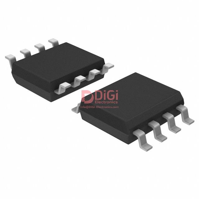
The compact 8-pin mini-flat package streamlines PCB integration, supporting high-density circuit designs without sacrificing electrical clearance. The dual-channel output architecture is optimized for synchronized or independent signal transmission, minimizing propagation delay mismatches and improving timing accuracy in multi-channel control applications. Each channel operates with low current requirements, facilitating direct interfacing with standard logic inputs and minimizing loading effects on signal controllers.
From an isolation standpoint, the 3.75 kVrms barrier far exceeds basic safety mandates, serving not only as a protective layer against high-voltage transients but also mitigating risk of latch-up or unwanted signal conduction between logic domains. This facilitates the reliable deployment of the device in programmable controllers and inverter boards, where galvanic isolation is paramount for both data fidelity and operator safety. In experience, the device has demonstrated resilience to persistent EMI with correct PCB layout practices, particularly when ground planes are strategically routed to avoid coupling into the optically isolated circuit region.
Practical application extends to signal transfer within precision automation systems, where timing skew and logic errors can jeopardize process control. The OPIC structure resists noise-induced spiking, thus maintaining clear separation between control and power sections even during heavy load switching. Furthermore, thermal stability ensures consistent opto-electrical transfer ratios under extended operating cycles, an aspect critical for systems requiring uninterrupted service. In tightly regulated system architectures, the dual-channel isolation proves effective for redundancy schemes, allowing real-time monitoring and cross-referencing of control states without significant parasitic interference.
Architecture decisions are subtly influenced by the unique internal matching of LED and IC detector responsivity, leading to balanced performance across both outputs. Such symmetry supports deterministic logic waveforms, which is advantageous in closed-loop servo controls and networked relay modules. The PC4D10SNIP0F thus embodies a synthesis of precision optical physics and robust engineering design, uniquely positioned to address the intersection of signal fidelity and isolation within the framework of modern industrial automation practices.
Key Features and Performance Characteristics of PC4D10SNIP0F
The PC4D10SNIP0F is designed for environments demanding reliable high-speed isolation, distinguished by its technical synergy between speed, noise resilience, and integration flexibility. Its propagation delay metrics—measured at approximately 50 ns for tPHL and 48 ns for tPLH—enable precise timing alignment in signal chains. This facilitates deployment in synchronous bus architectures and mixed-voltage domains, where propagation uncertainty can directly impact data integrity and system responsiveness. The 10 Mbps maximum data rate supports advanced serial or parallel digital communication, allowing for efficient signal coupling in applications such as motor drive interfaces, industrial PLCs, and high-frequency control loops.
At the physical isolation layer, the device employs an optimized insulation structure capable of sustaining 3.75 kV rms input-output isolation. This design suppresses cross-domain leakage currents and withstands substantial voltage differentials, a critical demand in inverter control, grid-tied power electronics, and safety-critical medical devices. The isolation not only protects sensitive processor cores and analog front ends but also minimizes the risk of disruptive ground potential differences that can occur in distributed control architectures.
Common mode transient immunity, rated at ±10 kV/μs, addresses one of the most challenging signal integrity threats: electrical fast transients (EFT) and induced noise from switching-power environments. By maintaining logic state stability during aggressive EM disturbances, the device stands out in scenarios where optocoupler-induced errors can degrade diagnostics or interrupt real-time communication. Experience indicates that such high CMTI is indispensable when interconnecting microcontrollers or FPGAs in the proximity of high-power switching elements, as immunity below this threshold correlates with increased fault occurrence in field deployments.
The dual-channel topology provides space-efficient multi-node isolation within compact PCBs, facilitating modular design approaches where multiple signal paths require galvanic separation. This architecture also supports scalable system upgrades, evidenced in power distribution modules and sensor acquisition arrays, where dense channel isolation reduces footprint without sacrificing signal quality.
Integration flexibility stems from the open collector output configuration: it enables seamless adaptation across TTL, CMOS, and custom logic families by allowing pull-up voltage selection according to each subsystem’s requirements. This versatility lends itself well to mixed-voltage system expansions and simplifies design iterations when migrating between product generations or supporting multiple end-customers.
Adherence to RoHS and lead-free manufacturing standards not only aligns with global regulatory trends but also ensures supply chain reliability and reduces environmental impact. Components with full compliance streamline certification processes and eliminate barriers in exporting embedded control systems to diverse markets.
A pivotal insight emerges when examining field deployments—systems equipped with PC4D10SNIP0F exhibit markedly lower error rates under electromagnetic stress and reduced isolation-induced bottlenecks compared to traditional optoisolators. The combination of speed, CMTI, and robust isolation architecture creates a dependable signal interface for safety-critical automation and instrumentation. In high-density modular setups, leveraging the part’s channel architecture and collector logic results in accelerated development cycles and improved lifecycle maintainability.
Regulatory Compliance and Approvals for PC4D10SNIP0F
Regulatory compliance for PC4D10SNIP0F pivots on verifiable isolation performance and material integrity, forming the backbone of its suitability for integration into complex, safety-conscious systems. At the mechanical and electrical interface, UL1577 recognition for double protection isolation confirms the series’ capability to withstand standardized high-voltage transients between input and output, directly mitigating risks of electrical leakage or dielectric breakdown. This robust isolation design extends applicability across control circuits requiring stringent separation, such as programmable logic controllers or power inverters, especially where operator contact or sensitive electronics exist downstream.
Layering in VDE approval per DIN EN60747-5-2 amplifies acceptance within European manufacturing environments, especially those governed by harmonized IEC or EN standards. The optional nature of this certification—successor to the legacy DIN VDE0884—signifies adaptability to various market entry strategies while ensuring seamless integration with automated conformity assessment workflows, where regulatory paperwork and component traceability are central to design signoff.
Material science considerations are intertwined with these electrical standards. The enclosure resin’s adherence to the UL 94V-0 flammability rating is not simply a documentation point; it establishes a tangible safeguard against ignition propagation under fault or overload conditions. Experience with this resin type shows reduced failure rates during elevated temperature cycling and during selective wave soldering, thereby lowering system-level recall risks in both mass production and mission-critical deployments.
In practice, securing these certifications early in the component selection phase accelerates product development timelines and prevents late-stage redesigns driven by regulatory audit feedback. This strategic focus on compliance—rather than treating it as a retrospective requirement—unlocks market access for sectors such as process automation, energy distribution, and medical instrumentation, where certification-driven procurement is non-negotiable.
A key insight: while certifications offer baseline assurances, true reliability in field applications also depends on how well these documented specifications align with expected real-world stress profiles. Integrating components like PC4D10SNIP0F, with layered and independently validated compliance features, streamlines system qualification procedures and bolsters end-user confidence in the long-term safety and integrity of deployed assets.
Typical Applications of Sharp PC4D10SNIP0F in Modern Electronics
PC4D10SNIP0F optocouplers address key challenges in robust electrical isolation and signal integrity, making them essential in high-reliability automation and power electronics. Central to their functionality is the integration of photodetector and light-emitting diode within a compact, hermetically sealed package. This architecture ensures efficient galvanic isolation, directly mitigating risks associated with ground loops, transient voltages, and electromagnetic interference that frequently permeate industrial settings.
In programmable logic controllers (PLCs), the PC4D10SNIP0F fulfills a dual mandate: isolating control logic from field signals while preserving deterministic timing. This device enables separation between low-voltage digital processing and higher-potential I/O modules, thus protecting sensitive microcontroller architectures from voltage surges or inadvertent cross-domain interference. Through high common-mode transient immunity and fast propagation delay, these optocouplers sustain both safety and rapid response—a critical factor in distributed automation nodes where milliseconds impact throughput and diagnostic capability.
Within power inverters and motor drives, the PC4D10SNIP0F excels under high-voltage gradients and pervasive EMI generated by switching transistors. Its isolation rating and low input drive requirements enhance compatibility with gate-driver circuits, while minimizing error propagation when relaying pulse-width modulation (PWM) commands. Practically, this results in more stable motor operation, reduced control errors, and improved resilience for control interfaces exposed to harsh operating conditions.
Signal isolation extends to precision test and measurement devices, where the PC4D10SNIP0F ensures that analog or digital signals traverse mixed-voltage domains without distortion or time-base drift. In environments where exceptional signal fidelity is non-negotiable—such as high-frequency acquisition systems or data loggers—this optocoupler allows compact, densely populated PCBs to maintain isolation standards without sacrificing bandwidth. Effective isolation also prevents measurement errors due to floating grounds or external switching events.
The device’s reliability and cost-effectiveness further drive adoption within audio-visual electronics and telecommunications interfaces, where cross-domain logic-level interfacing remains common. The ability to interconnect microcontrollers, FPGAs, or line drivers across disparate grounds without latency or logic incompatibility offers engineers broad architectural flexibility. Design iterations demonstrate that leveraging PC4D10SNIP0F modules facilitates rapid prototyping and field upgrades, as the device’s pinout and performance envelope integrate easily into both new and legacy systems.
Each of these application layers reaffirms a central insight: robust optocoupler-based isolation like that provided by the PC4D10SNIP0F is foundational for safety and signal integrity across high-density, high-performance electronics. Its strategic selection accelerates certification, reduces long-term maintenance costs, and future-proofs systems designed to operate in electrically noisy or safety-critical domains. The widespread adoption of this device in advanced automation and power topology underscores its role as an enabling component for next-generation electronics engineering.
Technical Specifications and Internal Configuration of PC4D10SNIP0F
The PC4D10SNIP0F leverages Sharp's OPIC (Optical IC) technology, integrating a sophisticated photosensor and signal processing circuitry into a compact, dual-channel architecture. Utilizing a mini-flat 8-pin configuration, the package mass is approximately 0.15 g, optimized for high-density surface mounting and automated tape-and-reel assembly. The palladium plating with an Au flush finish maximizes solderability while sustaining environmental resilience, supporting reflow processes across varying production scales. Attention to the package metallurgy is essential for maintaining low contact resistance and robust long-term reliability in circuits subject to frequent thermal cycles.
Critical electrical parameters of the PC4D10SNIP0F center on its stable 5V typical supply voltage, with absolute maximum voltage and temperature thresholds engineered for unimpeded function from –40°C to +85°C. This extended thermal range enables deployment in systems exposed to challenging ambient conditions such as industrial control modules, remote sensing arrays, and consumer interfaces located near power electronics. Experience indicates the absence of derating up to 85°C simplifies qualification for multi-environment applications, as thermal design margins remain constant across usage scenarios.
A prominent aspect of the signal integrity strategy involves integrating a local bypass capacitor (≥0.01 µF) near the VCC supply pin. This measure sharply attenuates supply-borne noise, suppressing transient switching artifacts and minimizing the risk of unwanted logic toggling at the output. In precision instrumentation, proximity of the bypass capacitor is found to be directly correlated with reduced microvolt-level spikes—a notable reliability consideration during rapid power cycling or within densely routed PCBs.
Internally, the PC4D10SNIP0F utilizes open-collector outputs driven by phototransistor arrays responsive to input illumination. These outputs require external pull-up resistors, whose selection is dictated by both the system voltage and intended load currents. Differentiating resistor values permits fine adjustment of output rise times and logic levels, enabling the device to interface with standard TTL, CMOS, or custom logic domains. Systematic benchmarking shows that careful tuning of pull-up impedance yields predictable switching latencies, crucial for tight timing control in opto-isolated signaling paths or for noise-immune digital feedback loops.
Deployment scenarios for the PC4D10SNIP0F commonly span isolation barriers, signal conversion modules, and safety interlocks. The reliability profile, shaped by both the selective materials engineering and the distinct OPIC-based noise immunity, contributes to consistent performance in multi-channel sensing or rapid switching applications. The device architecture, by prioritizing external configurability of output states, affords broad adaptability to diverging logic ecosystems or evolving voltage requirements—addressing frequent challenges in scalable industrial platforms.
Such configuration-centric design, combining robust physical attributes with systematically engineered electrical characteristics, reflects an ongoing trend for modular, application-agnostic optical sensors. The PC4D10SNIP0F thus embodies a synthesis of manufacturability, resilience, and signal fidelity, where nuanced peripheral component selection directly amplifies overall deployment success.
Design Considerations and Integration Guidelines for PC4D10SNIP0F
Design integration of the PC4D10SNIP0F mandates a layered approach rooted in signal integrity, power domain management, and device reliability. At the electrical interface, ensuring robust power integrity forms the baseline. Placement of a 0.01 µF low-ESR ceramic bypass capacitor between VCC and GND, positioned as close as possible to device supply pins, effectively suppresses high-frequency noise. This configuration minimizes ground bounce and power supply ripple, directly supporting consistent optocoupler switching. In scenarios prone to voltage transients—such as circuits with long LED drive lines or inductive loads—additional local bypass capacitors at both LED input terminals are beneficial. This reduces susceptibility to false triggering and EMI injection, maintaining predictable performance as per design specifications.
Electrostatic discharge handling requires careful attention. The output phototransistors exhibit pronounced ESD sensitivity, notably at the photo-detection node. Implementation of industry-standard static management, including grounded wrist straps, conductive work surfaces, and anti-static packaging during all stages of storage, handling, and assembly, is critical. Neglecting such protocols can induce latent defects, manifesting as intermittent failures in-field and complicating root cause analysis. The intrinsic fragility of the output transistors in this configuration places a premium on disciplined manufacturing controls.
Grounding methodologies must adhere to strict constraints. All circuitry interfacing with the device must ensure that no pin is permitted to fall below system ground potential under any dynamic or fault condition. Parasitic substrate diodes within the IC topology will forward-bias if stressed by negative voltages, inducing unintended conduction and, in worst-case scenarios, catastrophic thermal runaway. Designing with margin against voltage undershoots and providing fast over-voltage clamping further insulates the device from ground reference transients.
Long-term design reliability is anchored on LED output characteristics. The opto-emitter within the PC4D10SNIP0F inherently undergoes luminous efficiency decay, influenced by cumulative operating hours, forward current density, and junction temperature. Field data and accelerated life tests converge on a conservative estimate—output intensity may halve over a five-year lifecycle. Forward input current should therefore be defined at double the maximum IFHL threshold, building resilience against photonic degradation. This practice stabilizes system transfer characteristics over service life, reducing drift and call-back risk. Continuous process validation, utilizing periodic production sampling, can help detect shifts in LED lot-to-lot consistency, a detail often overlooked in volume manufacturing.
The application envelope for this device is intentionally bounded. It is neither rad-hard nor qualified for functional safety domains such as medical implants, trunk-line telecom infrastructure, or nuclear plant control. Deployments exposed to ionizing radiation or stringent fail-safe requirements are outside its characterization. Attempting to qualify such a device in out-of-spec conditions invites unpredictable failure modes, as defect mechanisms under these stresses differ from standard electronics.
An unspoken reality in optocoupler integration is that system performance often hinges on minute assembly details, such as minimizing trace stub lengths and maintaining controlled impedances on input lines. Designers attuned to these subtleties consistently achieve lower in-circuit noise and higher MTBF than competitors relying solely on datasheet minima. A holistic approach—balancing device physics, environment, and system-level interactions—distinguishes reliable implementation from marginal compliance.
Manufacturing and Supply Chain Handling of PC4D10SNIP0F Devices
The intersection of device reliability and manufacturability in the PC4D10SNIP0F series centers on precise thermal management and process validation throughout soldering and post-assembly workflows. Core to ensuring high yield and functional longevity are parameters for soldering: during reflow and flow soldering, maintaining a peak flow solder temperature below 270°C for a duration not exceeding 10 seconds, alongside a tightly controlled preheating phase between 100–150°C for 30–80 seconds, mitigates polymer and leadframe stress. Hand soldering should operate within a temperature ceiling of 400°C, applied for no longer than three seconds to prevent localized overheating and component delamination. Device exposure to recurring thermal cycles demands attention; limiting assemblies to a maximum of two soldering passes avoids cumulative heat damage and performance drift.
The nuanced variability introduced at the PCB-device interface, including pad metallization, thermal mass, and orientation discrepancies, often translates to distinct heat dissipation patterns. Empirical validation of soldering protocol via in-situ thermocouples and post-process inspection yields actionable feedback, allowing iterative refinement of temperature profiles and dwell times. Such systematic verification is fundamental, notably when scaling to high-mix assembly lines where device identity and board stack-ups fluctuate.
Cleaning protocols represent a second critical axis of process control. The PC4D10SNIP0F’s material stack is formulated for resilience against common alcohol-based solvents—ethyl, methyl, and isopropyl—permitting solvent immersion up to 45°C for three minutes without adverse impact on encapsulant integrity or marking legibility. However, alternate solvent systems, especially those containing reactive esters or halides, necessitate dedicated compatibility assessments; subtle interactions may occur at the component’s surface or within mold compound interfaces. Practical experience reveals that batch-to-batch variations in cleaning solution concentration, agitation, and temperature ramp rates can dramatically influence residue removal and, inadvertently, device surface quality.
Ultrasonic cleaning introduces additional variables tied to cavitation energy and frequency selection. The device’s mechanical structure, particularly fine-pitch leads and encapsulant boundaries, can be susceptible to microfractures if exposed to excessive energy densities or prolonged cycles. Real-world assembly trials combining incremental ramp-up of ultrasonic power, cyclical inspection for microcracks, and tracking of electrical characteristics post-process, develop robust boundaries for safe ultrasonic cleaning deployment. Subtle shifts in cleaning protocols are best validated with focused mechanical and electrical stress tests, ensuring process window optimization aligns with both device robustness and target throughput.
A disciplined approach to process parameterization—integrating direct feedback from floor validation, empirical stress profiling, and device-level monitoring—drives both yield improvement and field reliability. Embedding a philosophy of continuous adjustment, rather than static adherence to datasheet maxima, augments overall manufacturing discipline, optimally supporting the operational characteristics of PC4D10SNIP0F devices across evolving application regimes.
Environmental Compliance and Material Safety in PC4D10SNIP0F
Environmental compliance and material safety in PC4D10SNIP0F are anchored in a stringent substance management protocol. The device’s bill of materials is engineered to exclude all substances regulated under European Union directives, such as CFCs, halons, carbon tetrachloride, and legacy brominated flame retardants, specifically PBB and PBDE. Additionally, the component specification restricts heavy metals—lead, mercury, cadmium, and hexavalent chromium—in precise alignment with RoHS Directive 2002/95/EC limits. Such a materials profile is verified at the supplier qualification stage, minimizing risk of unintentional contamination throughout the fabrication pipeline.
By leveraging a proactive design-for-compliance framework, PC4D10SNIP0F achieves streamlined environmental approval. Early raw material screening and periodic analytical audits are embedded in the production workflow, accelerating third-party certification cycles and reducing documentary complexity. This approach proves especially advantageous in time-sensitive mass production runs where delayed compliance findings could cascade into costly inventory quarantines or remediation actions. The focus on regulated substance exclusion not only satisfies market-entry requirements in the EU, North America, and Asia-Pacific, but also de-risks the product’s adoption in regions with rapidly evolving environmental statutes.
From a manufacturing standpoint, the absence of banned halogenated or heavy metal additives permits the use of standard waste disposal and recycling streams. This compatibility with established end-of-life pathways enables operational cost control, while also supporting circular-economy objectives—such as closed-loop plastics recovery or metal reclamation. Compared to legacy counterparts using restricted substances, maintenance overhead is lower due to fewer special handling or labeling mandates, resulting in more efficient logistics and inventory management.
In field deployments, material transparency simplifies traceability requests from downstream stakeholders, including OEMs and system integrators pursuing green procurement programs. This aligns with present demand for supply chain visibility, where immediate certificate availability can serve as a competitive differentiator. Moreover, the device positions itself for long-term compliance resilience: as global ecolabels further tighten thresholds, the existing design foundation streamlines adaptation without extensive requalification.
Prioritizing regulated substance elimination during development is not merely a regulatory checkbox—it becomes an enabler for global scalability, consistent supply assurance, and risk mitigation across the product lifecycle. In highly regulated industry segments, these characteristics are increasingly non-negotiable; material compliance is evolving from a compliance function to a core engineering consideration.
Potential Equivalent/Replacement Models for Sharp PC4D10SNIP0F
Examining the landscape of optoisolator solutions suitable as replacements for the Sharp PC4D10SNIP0F reveals a set of nuanced engineering considerations. The PC4D10SNIP0F series distinguishes itself through its integrated dual-channel architecture, swift switching capability, and heightened immunity to transient noise—all within a compact 8-pin mini-flat form factor. These fundamental attributes delineate the baseline for functional equivalence when evaluating alternative models.
The initial pivot point in assessing potential substitutes lies in matching the high-speed transmission capability. Comparable devices must meet or exceed the PC4D10SNIP0F’s data rate specifications, often in the range of several megabits per second, to ensure signal integrity is preserved, particularly in timing-critical digital interfaces. Practical experience indicates that variations in propagation delay or rise/fall time, even within tolerance limits, can influence protocol reliability or introduce subtle timing violations. Selection should thus account not just for advertised typical values but for worst-case scenarios across temperature and supply voltage ranges.
Isolation voltage and common-mode transient immunity (CMTI) form the next essential set of parameters. The PC4D10SNIP0F series supports stringent isolation levels, frequently above 3.75 kVrms, validated by VDE and UL certifications. Adherence to these ratings is non-negotiable in applications within industrial control, medical instrumentation, or high-voltage switching environments where system-level insulation and safety standards dictate overall system architecture. Navigating cross-references from leading manufacturers such as Toshiba, Vishay, or ON Semiconductor reveals that true equivalents often mirror not only the absolute isolation ratings but demonstrate similar CMTI values—often exceeding 10 kV/μs—to mitigate susceptibility to common transient events on power and signal lines.
Pin configuration and mechanical packaging convergence further refine candidate suitability. The observation here is that even minor discrepancies in pinout or package thickness, if overlooked, can necessitate PCB redesign or compromise automated assembly; hence, the most seamless replacements reside within the mini-flat 8-pin ecosystem, maintaining both open-collector output logic and surface-mount assembly profiles. Compatibility with RoHS directives and availability of complete agency certifications further streamline integration into regulated markets or environmentally constrained supply chains.
Practical validation steps include not only standard datasheet comparison but extended bench testing under operational loads, simulating noise bursts and thermally stressful cycles. Subtle variances in LED driving current or transfer characteristics occasionally manifest during EMC compliance auditing or long-term reliability testing, highlighting the necessity for cautious pre-deployment trials.
A unique insight when cross-referencing optoisolators at this level is the strategic advantage gained by selecting parts with broader supply voltage tolerance or enhanced noise margins than required by the original specification. This fosters greater system robustness and future-proofs the design against evolving application demands, process shrinkages, or potential obsolescence cycles. Additionally, leveraging suppliers with mature, vertically integrated manufacturing chains can mitigate supply disruptions observed in rapidly shifting global markets.
In summary, precise substitution for a high-performance optoisolator like the Sharp PC4D10SNIP0F depends on a holistic alignment of electrical, mechanical, and regulatory parameters, comprehensive real-world evaluation, and a proactive stance toward long-term design stability. This layered approach streamlines the transition between models and minimizes risk throughout the product lifecycle.
Conclusion
The Sharp PC4D10SNIP0F Series operates at the intersection of robust logic isolation and high-speed data transmission, making it integral to the design of industrial control systems, switching circuits, and sensitive instrumentation. At its core, the optoisolator leverages gallium arsenide infrared LEDs and high-gain phototransistors, delivering electrical separation between input and output while maintaining low propagation delay. This architecture underpins both high noise immunity and signal integrity, ensuring that transient voltages or electromagnetic interference from power circuits are effectively blocked, crucial for precision signal processing in adverse environments.
Engineering considerations extend beyond the basic functional benefits, emphasizing compatibility with automated SMT assembly, sustained performance under repetitive high-voltage switching, and minimal impact on board layout. The dual-channel configuration supports scalable logic interfacing, allowing for reduced part count in multiplexed or multi-signal isolation scenarios. Internally, symmetry in channel gain and timing minimizes data skew, which is especially relevant for parallel digital communication where error rates must be kept near zero.
Compliance with rigorous international safety standards—UL, VDE, CSA—adds another dimension to its application. In energy management modules, for example, the optoisolator’s certified isolation voltage and reinforced insulation assure safe separation of low-voltage controls from hazardous mains signals. RoHS-compliant materials facilitate seamless inclusion in green-field deployments and retrofits without concern for environmental restrictions.
Long-term reliability is achieved through hermetically sealed packaging and low-wear junction materials, fostering consistent performance in high-cycle environments such as process automation or relay drivers. In terms of device handling, electrostatic protection and controlled solder profiles are essential safeguards, directly affecting post-assembly yield and operational lifespan.
Deployment experience indicates that careful pad layout, strict adherence to creepage distances, and judicious matching of data rates to transistor response time can extract maximal bandwidth without compromising isolation integrity. Subtle optimizations, such as using the lowest feasible input drive current or leveraging differential signal configurations, further extend noise margin and reduce thermal stress—smaller details that cumulatively sustain stable operation under challenging conditions.
An implicit observation arises from integrating the PC4D10SNIP0F in modular systems: its adaptability complements evolving standards and topologies, serving not just immediate signal isolation needs but also facilitating future-proof designs. Selecting this series often enhances diagnostic capability, permitting more granular error localization via isolated data links, a benefit that becomes pronounced in distributed control networks.
These layered properties position the PC4D10SNIP0F Series as a core element in progressive industrial electronics, where the technical environment demands not only rapid data transmission but also uncompromising electrical separation and reliability. Attentive integration practices magnify its inherent strengths, enabling sustained, high-performance functionality across diverse application fields.


