 >
>


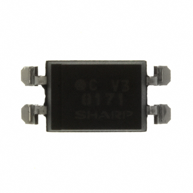
Product Overview: PC452 Series Optoisolators from Sharp Microelectronics
The PC452 Series Optoisolators from Sharp Microelectronics represent an integration of advanced optical coupling technology within a miniaturized SMD configuration. The heart of its mechanism relies on an infrared emitting diode (IRED) that transmits signals through a precise, controlled optical path. This IRED is intimately paired with a Darlington phototransistor stage, ensuring enhanced amplification and sensitive response to low-level optical input. The layered phototransistor array delivers high gain and consistent current transfer ratio even at low input currents, which intensifies system efficiency in low-power signal environments.
Through the adoption of a 3.75kV rms input-output isolation barrier, the PC452 bolsters circuit protection against unpredictable high-voltage surges. Its encapsulated package design minimizes creepage and clearance issues often encountered in densely packed PCB architectures. The optoisolator’s robust isolation capacity is critical for attenuating conducted and radiated electrical noise, particularly in mixed-signal control interfaces where transient immunity demands are stringent. The surface-mount format streamlines assembly, enabling higher board-level integration while reducing the risk of mechanical stress on solder joints during thermal cycling—an often-overlooked real-world reliability factor in continuous industrial operation.
Application scenarios for the PC452 extend from microcontroller I/O protection in programmable logic controllers to signal level shifting in power supply feedback loops and gate drivers for solid-state relays. The device’s 350V collector-emitter voltage rating supports direct interface with high-side or low-side switches, simplifying circuit topology and reducing external component count. Its capability to maintain signal integrity under high-voltage and high-noise conditions makes it particularly well-suited for factory automation, motor drive modules, and renewable energy inverter products, where isolation must keep pace with rapid switching edges and broad dynamic voltage swings.
A frequently realized benefit emerges in field deployments requiring rigorous electromagnetic compatibility (EMC). With the PC452’s high isolation voltage and compact footprint, integration within complex system layers is achievable without sacrificing channel density or risking cross-talk. During testing phases, consistent transfer performance across temperature and input variations indicated solid parametric stability, minimizing recalibration needs and supporting long service intervals. The use of Darlington phototransistor topology, rather than a standard single-transistor scheme, implicitly pushes noise margins further and permits operation within lower input drive budgets.
In summary, the PC452 Series delivers a refined, multi-layered approach to optoelectronic isolation, combining physical ruggedness with electrical robustness and architectural efficiency. Its suitability for high-performance digital and analog isolation exemplifies the convergence of reliability with miniaturization. The design choices embedded in this series, such as isolation barrier integrity and Darlington amplification, point toward an implicit understanding of the evolving requirements in modern electronic system engineering, enabling scalable and resilient solutions across the entire spectrum of demanding control and power management scenarios.
Key Features of the PC452 Series
At the heart of the PC452 Series lies a meticulously engineered set of attributes tailored for advanced isolation requirements in dense electronic architectures. The adoption of a mini-flat 4-pin surface mount package directly addresses the spatial constraints prevalent in contemporary system boards, enabling tighter packing density without compromising electrical clearance or creepage distances. This packaging not only facilitates integration into multilayer PCBs but also simplifies automated assembly processes, supporting high-throughput manufacturing environments.
The double transfer mold package construction enhances mechanical resilience and guarantees product integrity, especially under cyclic thermal and mechanical stress encountered during standard flow and reflow soldering. By optimizing the encapsulation material and geometry, the package achieves superior moisture resistance and long-term reliability—key factors in mission-critical applications where field failures are not tolerable.
Equipped with a Darlington phototransistor output, the PC452 Series delivers an exceptionally high current transfer ratio (CTR) of 1000% at a mere 1mA input. This configuration amplifies input-side current with minimal power overhead, ensuring responsive signal detection even in low-current drive scenarios. Such sensitivity allows for accurate interfacing with high-impedance control circuitry and accommodates broad variations in input signal levels without risking data loss or misinterpretation.
A high collector-emitter voltage rating ($V_{CEO}$ of 350V) further extends the applicability of the series, making it suitable for interface designs where voltage excursions or transients are anticipated. This elevated voltage threshold allows the device to bridge logic circuits and high-voltage domains efficiently, mitigating the risk of breakdown and supporting robust protection schemes in mixed-signal environments.
The input-output isolation voltage of 3.75kV rms is integral for safeguarding sensitive logic from disruptive voltage transients and ensuring galvanic decoupling between disparate system blocks. This isolation performance aligns with stringent regulatory demands in industrial and communication sectors, enhancing overall system safety and noise immunity. The ability to withstand high common-mode voltages while preserving low propagation delay is especially beneficial in differential signaling applications and power line communication interfaces.
In real-world implementations, the combination of board space efficiency, process compatibility, and electrical robustness in the PC452 Series accelerates system-level validation and scalability. When deployed in hybrid substrates, copiers, or communication interfaces, the component’s compact profile streamlines thermal management and facilitates denser routing without elevating cross-talk or leakage risks. Additionally, the consistent CTR and reliable isolation substantially reduce engineering overhead related to margining and derating—enabling smooth migration from prototyping to production.
Careful attention to CTR consistency and isolation durability positions the PC452 Series as a core building block for designers seeking to optimize both performance and footprint in applications ranging from distributed control systems to compact embedded modules. Maximizing board real estate while maintaining stringent isolation and high signal integrity emerges as a strategic advantage, defining the PC452 Series as a preferred choice in next-generation electronic assemblies.
Electrical and Electro-Optical Characteristics of PC452
A detailed analysis of the PC452 series highlights several intertwined electrical and electro-optical attributes that serve demanding precision isolation scenarios. The architecture features robust input-output isolation, rated at 3.75kV rms. This threshold is essential in mixed-voltage environments, where safeguarding low-voltage microcontroller domains from potentially disruptive high-voltage transients is paramount. Isolation parameters not only dictate compliance with industrial safety standards, but also expand possibilities for inter-system interfacing in noisy or high-energy settings.
Optoelectronic coupling in the PC452 leverages an optimized Darlington output stage, delivering a minimum current transfer ratio (CTR) of 1000% at just 1mA forward current and 2V collector-emitter voltage. This performance enables the use of high-resistance input drive circuits, minimizing auxiliary power draw, an asset for energy-conscious designs or densely populated boards. The Darlington configuration amplifies the phototransistor’s inherent sensitivity, ensuring that even modest LED currents are converted into decisive output levels. This is particularly beneficial where direct logic compatibility is required without resorting to additional amplification stages.
Voltage handling capabilities form another pillar of the PC452’s versatility. With a collector-emitter voltage ceiling of 350V, the device accommodates a wide spectrum of switching and interfacing roles. Applications such as industrial PLC inputs, relay drivers, or voltage monitoring often demand both logic-level response and tolerance for moderate overvoltage conditions, a balance the PC452 strikes reliably. The expansive voltage window broadens application domains while maintaining switching integrity even in fluctuating field environments.
It is essential to factor in the operational nuances that may affect device behavior. Characteristic curves provided in documentation reveal explicit dependencies: both CTR and response speed show deterministic shifts with varying ambient temperature, input forward current, and load resistance. In real-world deployments, thermal gradients and fluctuating supply conditions can introduce latency or influence signal fidelity. For instance, response times will slacken with higher load resistance, a trade-off that must be considered in timing-sensitive links. Minor derating of CTR at elevated temperatures is often observed, urging the implementation of headroom in critical signal paths or the selection of bias currents aligned with worst-case scenarios.
Experience shows that embedding the PC452 in densely-packed industrial panels exposes it to transient temperature swings and electromagnetic interference. The benefit of the device’s high minimum CTR is most tangible when interfacing with logic controllers featuring limited current sourcing capability, or when bufferless driving is desired. Furthermore, the consistent isolation voltage rating provides confidence during regulatory approvals for products requiring reinforced insulation.
From a systems perspective, the synergy between high isolation, aggressive transfer efficiency, and broad voltage handling renders the PC452 adaptable to diverse automation, communication, and process control schemes. By reviewing the detailed performance curves pre-layout and biasing the device to exploit its linear response regions, implementations can achieve both reliability and low power overhead. Selecting such a photo-isolator enables streamlined PCB architectures, reduces the need for peripheral components, and permits scalable expansion into multiple isolation channels with a repeatable footprint.
Integrating these elements, the PC452 extends value through both foundational electrical fortitude and nuanced application flexibility. Its high-efficiency optocoupling and rugged voltage margins set it apart for designers seeking to balance cost, performance, and design risk in critical isolation applications.
Mechanical Construction and Packaging Details for PC452 Series
Mechanical integrity in PC452 series optoisolators arises from a carefully engineered double transfer mold package, which maximizes robustness during both thermal cycling and demanding reflow soldering environments. This encapsulation technique mitigates microcracking and substrate delamination—two failure modes prevalent in high-temperature processing. The result is a consistent yield through sequential manufacturing steps, especially as assemblies undergo multiple soldering passes typical of high-density board designs.
The mini-flat SMD outline, at approximately 0.1g, optimizes for automated placement systems without sacrificing board utilization. Tape-and-reel packaging in standardized reels, such as 3,000 or 750 unit counts, aligns directly with surface-mount workflow requirements, enabling continuous feeding for high-speed pick-and-place lines. Inventory control is streamlined due to predictable reel sizes, supporting lean manufacturing models and reducing handling-induced component attrition.
Pin assignments, clearly defined as Anode, Cathode (input side) and Emitter, Collector (output side), standardize integration on multi-layer PCBs. The explicit mapping expedites layout and reduces the likelihood of routing errors in schematic capture and foot-print definition. Mechanical registration between pad geometry and package leads maintains coplanarity, essential for minimizing tombstoning and other solder joint anomalies during reflow.
Throughout board assembly—whether utilizing fully automated robotics or selective manual intervention—the PC452 package preserves compatibility with most industry-standard solder paste alloys, fluxes, and cleaning cycles. Moisture sensitivity level (MSL) compliance and low-profile geometry further reduce warpage risk and enhance the component’s tolerance for regulatory cleaning solvents, a consideration often overlooked but critical to long-term reliability.
Practical deployment demonstrates that optimizing pick nozzle design and setting component thickness parameters for feeders yields notable enhancement in line throughput. Careful management of thermal profiles during reflow prevents excessive mechanical stress, ensuring consistent encapsulation integrity and lead adhesion.
It is increasingly apparent that the mechanical construction and packaging strategy of the PC452 series directly influences downstream electrical performance and lifecycle reliability. By harmonizing mass production constraints with robust packaging technologies, the design not only streamlines integration in tightly constrained layouts but also engenders confidence for use in mission-critical industrial, consumer, and automotive control circuits.
Agency Approvals and Regulatory Compliance of PC452
Agency approvals and regulatory compliance are central in the deployment of optical isolators such as the Sharp PC452 Series, especially in critical industrial and consumer electronics applications. The series achieves double protection isolation as verified by UL1577 (UL file No. E64380), substantiating its suitability in circuits demanding robust galvanic separation. This depth of certification is essential for meeting requirements in safety-critical designs, including medical power supplies, industrial control systems, and smart metering, where regulatory scrutiny focuses not only on electrical performance but on isolation integrity under fault conditions.
The encapsulation resin of the PC452 Series holds the UL 94V-0 flammability rating, a material property that signifies rapid extinguishing and low combustion risk. In real-world design cycles, this rating expedites device selection for end products targeting international safety marks such as CE, CB, and IEC/EN compliance. The practical advantage manifests in streamlined approvals for final assemblies, as the optocoupler’s enclosure directly supports overall equipment pass-through in system-level flame tests—a common hurdle in initial certification audits.
Attention to environmental substance restrictions represents an advanced approach to product stewardship. The PC452 Series is manufactured without the inclusion of CFCs, Halon, carbon tetrachloride, methylchloroform, and brominated flame retardants (PBBOs and PBBs). This proactive exclusion aligns with RoHS, REACH, and similar regulatory frameworks, ensuring that device integration does not introduce compliance risks related to material compositions. In multi-regional supply chains, such intrinsic material conformance reduces the need for costly retesting or secondary validation, shaving weeks off product release timelines.
The confluence of robust isolation, superior flame resistance, and certified substance exclusion translates to quantifiable benefits in the field. Designers typically integrate PC452 optocouplers in interfaces between high-voltage and low-voltage domains, where agency listings serve as assurance during functional safety evaluations or customer audits. The hardened isolation and documented safety features often minimize concerns related to creepage, clearance, and long-term reliability, providing peace of mind when scaling up designs for automotive, energy, and industrial automation sectors.
Reliance on deeply certified components like the PC452 Series demonstrates a shift in engineering priorities towards embedded compliance. Rather than retrofitting safety into legacy designs, modern development processes now select optoelectronic isolators with verified protections from the outset. This preemptive strategy accelerates total project timelines, supports modular platform development, and increases the likelihood of first-pass approvals by both internal QA teams and external inspection bodies. The layered certification of the PC452 Series thus functions as not only a technical safeguard, but also a strategic asset within the competitive product development cycle.
Application Scenarios for PC452 Series Optoisolators
The PC452 Series is engineered for circuit environments that demand reliable and compact galvanic isolation, coupling logic signals across disparate voltage domains without direct electrical continuity. Its mini-flat package facilitates straightforward integration into dense PCB layouts, minimizing board real estate consumed by isolation interfaces. At the device level, the PC452 achieves high common-mode transient immunity via optically coupled input/output stages, preserving data integrity even in environments with significant ground potential differences or high-voltage transients.
In telecommunications equipment such as telephone sets and facsimile units, the PC452 optoisolator effectively decouples low-voltage digital control logic from high-voltage ring or line signals. The device’s robust insulation characteristics meet regulatory standards, preventing crosstalk and reducing susceptibility to induced surges. Practical deployment in these systems consistently demonstrates stable system operation and minimizes noise pickup, particularly critical in regions with variable line quality.
Distribution boards and power interfaces present another compelling application. The high isolation voltage and elevated current transfer ratio (CTR) of the PC452 allow reliable monitoring and control between low-level logic controllers and mains-level circuits. This ensures that microcontroller outputs are shielded from potentially destructive power-line disturbances. The CTR uniformity contributes to predictable opto drive requirements, simplifying input stage design and facilitating robust, maintainable schematics.
Hybrid substrates and high-density assemblies benefit noticeably from the mini-flat form factor of the PC452, which enables placement in proximity to signal sources or sinks without sacrificing board accessibility for testing or rework. In practice, this footprint compatibility accelerates iteration cycles during development and supports long-term maintainability in mass-produced modules.
In office automation and industrial control, system reliability and electrical noise immunity are key. The PC452’s fast switching and minimal propagation delay enable fail-safe signal transfer within PLCs and actuator control boards. This feature is especially significant in multi-channel feedback systems, where propagation delays and cross-channel interference can compromise process accuracy. Deployment experience often reveals lower error rates and reduced downstream component stress when replacing legacy isolators with modern mini-flat solutions like the PC452.
When deploying PC452 in new design platforms, strategic placement of bypass capacitors and meticulous PCB trace layout are crucial for maximizing the noise rejection and insulation performance. Notably, the device’s performance envelope supports both legacy 5V digital logic and modern low-voltage signaling standards, ensuring project flexibility and forward compatibility.
Adaptation of the PC452 across these domains reveals its role as both a space-optimizing and a functionally robust isolator—an optimal match for engineers seeking reliable, low-footprint solutions where galvanic isolation is non-negotiable. The balance of high isolation voltage, consistent CTR, and minimal package dimensions yields versatile applicability, especially in tightly regulated or space-constrained environments where both performance and regulatory compliance are paramount.
Design Considerations for Engineering with PC452
Designing with PC452 optoisolators demands close examination of their electrical and physical characteristics, starting from first principles of optoelectronic interaction to system-level deployment. At the device level, current transfer ratio (CTR) stability is intrinsically linked to the forward current applied to the input IRED. When forward current drops below 1.0mA, statistical and material variations significantly increase relative CTR distribution, which can give rise to unpredictable switching thresholds. Thus, threshold calculations should incorporate not just datasheet values but also the potential for greater deviation at low drive currents, favoring circuit architectures that allow for adjustable or margin-enhanced input stages. Experience shows that designing with an initial operating current above the CTR inflection point results in greater long-term consistency and simplifies failure mode analysis.
Addressing long-term reliability, the IRED emission degrades over time, commonly approaching 50% loss over a five-year period in standard conditions. This photometric decay directly reduces the output CTR, potentially compromising signal integrity or causing erratic operation in safety-critical scenarios. Successful engineering strategies include specifying the minimum required CTR at end-of-life, rather than at initial deployment, and selecting the device bin accordingly. Circuit designs should build in headroom for this degradation, for instance by setting higher input currents initially or integrating feedback-based aging compensation, to avoid premature wear-out and reduce service calls in maintenance-averse installations.
From a signal integrity and isolation perspective, practical deployment in high-frequency environments introduces additional layers of complexity. The frequency response of the PC452, along with maximum output saturation voltage, determines both bandwidth and noise immunity. It is essential to review the transfer characteristics across the intended operating temperature and power supply ranges, ensuring that device placement on the PCB does not inadvertently couple noise into the optoisolator channel or stress its isolation barrier. Strategic component placement and trace routing, informed by application notes and empirical signal analysis, mitigate timing skew and crosstalk. Optimal loading further minimizes propagation delay and voltage drops, maintaining system reliability in fast-switching designs.
The mechanical attributes of the PC452, such as its mini-flat footprint, facilitate integration into high-density boards. However, past implementations underline the value of meticulous adherence to recommended footprint patterns—accounting for solder joint reliability, thermal cycling, and creepage distances—to sustain both electrical performance and mechanical integrity through the product lifecycle. Utilizing proven PCB land patterns and verified stencil designs optimizes manufacturability and reduces rework risk during production ramp-up.
In summary, the robust implementation of PC452 optoisolators hinges on a holistic design mindset—balancing drive conditions, device aging, high-speed performance, and assembly constraints. Prioritizing system margins and aligning layout with manufacturer guidance ensures reliable function across a broad spectrum of application scenarios.
Manufacturing and Soldering Guidelines for PC452 Series
Manufacturing and assembly of the PC452 Series necessitate adherence to stringent soldering protocols and thermal management, directly anchored in the device’s double transfer mold package construction. The robust mold design is specifically formulated to sustain industry-standard reflow and flow soldering, yet retains sensitivity to excessive thermal cycles. Notably, soldering is limited to no more than two passes. This restriction mitigates the risk of semiconductor junction degradation—a failure mode often observed when interfacial stress exceeds design thresholds due to repeated heating or uneven cooling rates.
Reflow soldering demands strict compliance with the profile recommended by Sharp, focusing on controlled ramp-up, dwell, and cooling stages. These steps are essential for consistent alloy wetting and preventing voids at the solder joint. Flow soldering, enabled by the package’s enhanced mechanical resilience, allows exposure to up to 260°C for a period not exceeding 10 seconds, following a preheat window of 100–150°C. This regimen supports uniform heat distribution, crucial for minimizing thermal gradients across the die and molding interface which, if unmanaged, could cause warping or delamination.
Hand soldering, while permissible for limited field repairs or specialized assembly, requires that contact be restricted to below 3 seconds at tip temperatures not above 400°C. This tightly constrained protocol reflects empirical data showing that prolonged exposure, even at seemingly moderate temperatures, is a primary contributor to compromised bond integrity, leading to increased risk of long-term reliability losses.
Increased attention to process validation is warranted. Pilot assembly runs and real-world PCB loading studies provide indispensable feedback for fine-tuning thermal profiles and contact times, revealing latent susceptibilities to mechanical or thermal stress. Such iterative validation also supports yield optimization by exposing subtle process-induced variances—such as solder creep or flux residue—that standard qualification may overlook.
Automated lines, leveraging reflow and flow soldering, derive maximal benefit from these guidelines through repeatable, high-throughput cycles with low defect rates, while manual operations—where variability is inherently higher—are protected by clear time and temperature windows. The interplay between package integrity, thermal exposure, and process discipline forms the core of reliable long-term field performance in diverse application contexts. Integrating experience-driven feedback at each stage fosters process resilience, ensuring sustained manufacturability as device geometries and board layouts continue to evolve.
Underlying these protocols is the insight that package-level robustness does not obviate the need for precise soldering discipline; even advanced molding can be undermined by marginal overexposure or procedural lapses. The cumulative impact of disciplined thermal management and structured validation translates directly to lower latent defect rates and extended functional lifetimes of the assembled product.
Cleaning, Environmental, and Regulatory Information for PC452
Post-assembly cleaning protocols for PC452 are configured to maintain operational stability and extend lifecycle reliability. The fundamental approach relies on the use of approved organic solvents—ethyl alcohol, methyl alcohol, or isopropyl alcohol—where critical process parameters include strict thermal control not to exceed 45°C and an immersion period limited to three minutes. Prolonged exposure or elevated temperatures risk undermining encapsulant strength and component adhesion, potentially initiating microscopic fissures or solvent-induced stress that would only become apparent during late-stage quality evaluations or field operation.
Ultrasonic cleaning introduces further considerations, primarily due to the interplay between frequency, power output, and device encapsulation characteristics. Tolerance verification for each batch is imperative, given that acoustic cavitation and liquid agitation can exhibit non-linear effects on device substrates and interfacial bonding. Empirical evidence demonstrates that minor variations in system calibration or tank loading density contribute to disparate outcomes—ranging from benign particle removal to detrimental delamination—underscoring the necessity for tailored batch-wise validation complemented by post-process functional assessment.
The PC452 device’s design philosophy prioritizes environmental responsibility by excluding ozone-depleting substances and banned halogenated flame retardants. This aligns with global standards such as RoHS and REACH, minimizing regulatory compliance risks and supporting integration into end-products destined for markets with rigorous ecological mandates. Embedding these environmental controls at the component level has yielded measurable advantages in downstream process optimization, particularly in multi-tier supply chains where traceability and auditability of hazardous substances are routine customer requirements.
Sustained adherence to specified cleaning and handling protocols directly supports both internal production efficiency and external certification. Deviations, especially in process consistency, have proven to amplify residual ionic contamination, ultimately influencing long-term surface insulation resistance and increasing the probability of intermittent field failures. In high-reliability sectors, such as automotive or industrial controls, empirical process tracking coupled with disciplined enforcement of cleaning regimes is recognized as a determinant of elevated product yield and minimized warranty exposure.
Proactive integration of robust cleaning and environmental strategies into the PC452’s manufacturing lifecycle exemplifies the convergence of quality engineering and sustainability. This multifaceted approach not only protects device performance but also anticipates evolving regulatory landscapes and end-customer expectations, reinforcing the strategic significance of early and precise protocol implementation.
Potential Equivalent/Replacement Models for PC452 Series
When approaching the selection of substitutes for the PC452 series, it is essential to dissect the functional requirements tied to isolation, output topology, and package constraints. The underlying operational imperative is maintaining galvanic isolation compliant with safety or EMC standards, making isolation voltage a non-negotiable specification. The PC452’s 3.75kV isolation voltage, coupled with its mini-flat package, addresses compact PCB designs requiring robust physical and electrical separation. In practice, any candidate replacement must be scrutinized for both its withstand voltage and its certification footprint, ensuring compliance with global standards such as UL or VDE. Overlooking subtle differences in creepage or clearance dimensions can drive significant requalification cycles, especially in industrial or consumer end-products subject to regulatory audits.
Signal transfer characteristics govern parametric equivalence. The PC452’s Darlington output stage delivers high current transfer ratio (CTR), optimizing drive capability at low input currents and enabling efficient low-side or high-voltage switching. Cross-comparing CTR at matched input currents between alternative models is critical, as deviations alter LED drive circuitry, impacting overall power budget and switching thresholds. Devices sourced from other manufacturers—Lite-On, Toshiba, or Vishay—frequently align on nominal CTR targets but exhibit meaningful spread in minimum or maximum specifications. Empirical evaluation in the target topology, especially where input drive headroom is limited, often exposes subtle behavioral differences including turn-on voltage and CTR degradation over temperature or operating lifetime.
Attention to collector-emitter voltage ratings is equally critical. The PC452’s 350V maximum Vce enables interfacing with high-voltage rails or robust signal paths across relay drivers, data acquisition isolation barriers, and power supply feedback loops. Substitutes must not only match this absolute rating but also withstand repetitive surges and transient overvoltage scenarios common in industrial or automotive applications. Margin should be maintained to accommodate real-world derating requirements, which are sometimes more stringent than datasheet limits suggest.
Package size and pin configuration drive the practical interchangeability of optoisolators. The mechanical footprint must slot into existing PCB layouts with zero or minimal modification. Even subtle changes in lead geometry, pin pitch, or plastic encapsulation may challenge automated assembly or impact solder joint reliability. Models from vendors such as ON Semiconductor or Everlight occasionally differentiate themselves with process enhancements like improved lead-forming or moisture resistance, which warrant consideration for designs in demanding environmental conditions.
Certification requirements complete the equivalence matrix. Regulatory acceptance hinges on externally documented compliance, not merely electrical performance. Opting for parts with matching or broader approvals accelerates qualification, limits re-test costs, and secures ongoing certification for end equipment.
The selection process for a PC452 alternative is thus multi-dimensional. Beyond datasheet comparison, real-world application stresses—thermal cycling, input drive variability, voltage surges, and board-level assembly—must inform sourcing choices. The convergence of optical coupling parameters, mechanical interchangeability, and certification assures robust supply chain diversification without incurring hidden integration or compliance penalties. In current supply environments marked by lead time fluctuations, strategic consideration of second-source readiness and long-term availability delivers engineering agility amid evolving procurement realities.
Conclusion
Selecting the PC452 Series optoisolators involves analyzing core operational mechanisms and correlating product parameters with application contexts demanding signal isolation. At the foundational level, the PC452 deploys a phototransistor output, tightly coupled to an LED input via a high-dielectric barrier, presenting isolation voltages suitable for systems with demanding safety profiles. This construction directly mitigates transient voltage risks and ensures robust galvanic isolation between control and load domains, a critical feature in power conversion or industrial automation circuits.
Performance metrics such as current transfer ratio (CTR), input-output response time, and operating temperature range further elevate device versatility. The high CTR provided supports efficient signal coupling even under low input current regimes, which is essential in energy-sensitive designs and ensures logic compatibility across varied platforms. Fast switching times and minimal propagation delay allow for reliable state changes in bidirectional communication links, directly impacting throughput and timing integrity in protocols like RS-232 or CAN bus.
Safety compliance, evidenced by international certifications embedded within the PC452 datasheet, streamlines the integration process into equipment bound by regulatory frameworks. These certifications not only facilitate approval cycles, but instill long-term reliability, particularly in installations requiring maintenance-free lifespans or adherence to fail-safe operation standards. Attention to creepage and clearance distances in surface-mount layout further assists in meeting regulatory demands for high-voltage isolation, with real-world assembly processes benefiting from the SMD form factor’s reflow compatibility and minimized parasitic inductance.
Experience indicates that leveraging the PC452’s design flexibility—such as its tolerance for automated pick-and-place and reflow cycles—helps reduce both assembly time and process-induced failures, a key driver for high-volume manufacturing return. Engineers can realize system reliability enhancements when integrating these optoisolators into feedback and interlock circuitry, where signal integrity and electrical isolation constitute undebatable priorities.
Evaluating lifecycle factors, the PC452’s standardized form and lead-free composition align smoothly with contemporary environmental directives, supporting backward integration into legacy systems. Realistically, its consistent parametric performance over extended operational hours supports long-term cost optimization, making maintenance forecasting more predictable and bill of materials management more streamlined.
In embedded control, renewable energy management, or motor drive electronics, optoisolators like the PC452 reveal their true value in scenarios where cross-domain signal transmission must occur without sacrificing fault containment. The convergence of robust isolation, responsive control, and direct manufacturability affirms the PC452 Series as a technical asset for forward-looking circuit architectures. Strategic device selection, rooted in a precise match of system safety requirements and physical design constraints, ultimately enhances the reliability and operational clarity of the engineered solution.