>
>


Product overview: PC3Q710NIP optoisolator series from Sharp Microelectronics
The PC3Q710NIP optoisolator series from Sharp Microelectronics delivers robust multi-channel galvanic isolation essential for advanced electronic systems in industrial and commercial domains. This quad-channel device integrates phototransistor outputs, providing a reliable interface for transmitting digital or analog signals across high-potential differences. Leveraging Sharp's optoelectronic process technology, the PC3Q710NIP achieves high common-mode transient immunity, a critical attribute for environments with substantial electrical noise or variable ground potentials. Such immunity is engineered at the device level through precise internal layout that minimizes capacitive coupling, thus suppressing transient interference within and between channels.
In the context of high-density PCB layouts, the 16-Mini-Flat SOIC package enables significant space savings while permitting straightforward routing and assembly. Thermal management is optimized by the low-power consumption profile per channel, maintaining operational stability even in tightly packed configurations. The uniformity in channel performance—rooted in stringent manufacturing calibration—ensures predictable propagation delays, which is particularly valuable in timing-sensitive digital interfaces such as SPI, I²C, or custom parallel data buses. These features collectively simplify signal integrity management across isolated logic boundaries.
Within industrial automation, motor drive control systems benefit from the optoisolator’s voltage-withstand capability, often exceeding 3.75 kVrms, safeguarding low-voltage microcontroller domains from high-voltage actuator arrays. In medical instrumentation, the device’s multi-channel integration reduces channel-to-channel skew and board-level component count, supporting simultaneous monitoring lines with minimal crosstalk risk. The SOIC package footprint aligns with automated optical inspection requirements, further tightening quality assurance in volume production settings.
One foundational insight centers on the synergy between isolation rating and switching speed. While safety mandates high VM isolation, these devices also balance fast response times, facilitating compact and scalable solutions in dynamic environments. Direct deployment experience has highlighted the importance of adhering to recommended PCB layout practices, such as maintaining adequate creepage and clearance around the SOIC package and incorporating ground shielding where channel isolation is paramount. Consistent logic-level output and low saturation voltage across channels reduce system-level calibration complexity.
The core advantage of the PC3Q710NIP lies in its capability to streamline multi-path isolation needs for data acquisition, programmable logic controllers, and instrumentation interfaces. By unifying isolation and drive functionality within a minimized form factor, the device supports the ongoing shift toward modular and miniaturized system architectures without sacrificing electrical safety or signal fidelity.
Features and technical specifications of PC3Q710NIP
The PC3Q710NIP series integrates four discrete optoisolation channels in a unified package, targeting high-reliability system architectures where robust electrical isolation and signal integrity are crucial. Each channel employs a high-efficiency phototransistor output, establishing galvanic separation between the input and output circuits. This architecture eliminates common-mode noise coupling, mitigating risks associated with transients and ground loop-induced disturbances. Rooted in a rated isolation voltage of 2500Vrms, the device effectively withstands differential voltages encountered in industrial and precision control applications, enhancing the system’s resilience to surges and cross-domain interference.
Optoisolation in PC3Q710NIP is optimized for low propagation delay and consistent channel-to-channel performance, establishing reliable communication across system nodes with divergent ground references. A consistent output switching characteristic simplifies timing analysis in synchronous designs, while integrated noise rejection mechanisms suppress parasitic switching events. The selection of a phototransistor output streamlines interfacing with TTL, CMOS, and LVC logic families, directly accommodating standard signal levels without the need for additional line drivers or level shifters. This expedites schematic integration and layout flow, especially where compact multi-channel isolation is required.
Practical deployment of the PC3Q710NIP reveals stable operation even under significant electromagnetic interference, as verified in systems subjected to routine high-speed switching transients. In densely populated control cabinets, leveraging the four-channel configuration reduces component count and board space compared to discrete solutions, promoting higher assembly yields and improved long-term reliability. These benefits prove significant in PLC input modules, AC drive feedback loops, and process control networks, where robust optical isolation is non-negotiable.
Engineering decisions frequently weigh optoisolator saturation characteristics, response times, and CTR (Current Transfer Ratio) stability. PC3Q710NIP demonstrates low saturation voltages and consistent CTR across specified operating ranges, reducing signal distortion in extended duty cycles and minimizing errors in precision conversion schemes. This positions the device favorably for scalable architectures—whether in expansion of digital inputs or modular sensor interfaces.
Distilling practical experience and technical analysis, the PC3Q710NIP distinguishes itself by aligning optical isolation fundamentals with modern signal chain requirements, providing a multidimensional solution to isolation, integration density, and application versatility. Such features directly elevate the reliability and maintainability of mission-critical electronic systems.
Electrical characteristics and isolation performance of PC3Q710NIP
The PC3Q710NIP optoisolator integrates robust electrical isolation with reliable signal transmission. Its primary mechanism relies on the optical coupling principle, wherein a phototransistor responds to the input-side infrared LED, converting optical signals into electrical ones without establishing a direct conductive path. This underpins the device’s core isolation voltage—2500Vrms AC between input and output—enabling its deployment in circuits exposed to substantial voltage differentials. This level of isolation is vital in industrial environments prone to transient surges and ground potential fluctuations, as it effectively suppresses common-mode noise and fault propagation.
In practical engineering scenarios, the PC3Q710NIP excels in feedback control loops of switch-mode power supplies. The isolation barrier secures low-voltage controller circuits from unstable high-voltage switching nodes, a frequent source of catastrophic failures in designs lacking adequate protection. Within power management frameworks, this optoisolator prevents error signals from being corrupted by EMI or high-voltage spikes, thus sustaining regulation accuracy. Experience demonstrates that careful layout practices, such as maximizing the creepage distance on PCBs and optimizing LED drive current, further enhance device performance and long-term isolation reliability—critical considerations in safety-driven applications.
From a functional viewpoint, the PC3Q710NIP’s transistor output structure yields fast switching speeds and consistent saturation characteristics, supporting both rapid on-off logic transfers and precise transmission of analog or pulse-width modulated signals. This attribute allows seamless interface between microcontrollers, data acquisition modules, and high-voltage loads, sidestepping the trade-offs commonly encountered when integrating discrete isolation and driver stages. The absence of direct galvanic connection eliminates ground loops, which are endemic in complex industrial and instrumentation networks, thus preserving signal fidelity and reducing system-level troubleshooting.
In advanced applications, such as multi-channel signal routing or isolated sensor interfaces, the device’s high isolation voltage and stable switching behavior mitigate risks associated with cross-channel leakage and unintentional signal coupling. By leveraging these characteristics, designers can extend the operational lifespan and predictive reliability metrics of their assemblies. The key insight is that implementing high-grade optoisolators like the PC3Q710NIP not only protects electronics but also simplifies circuit complexity, offering a direct pathway to robust, scalable system architectures in high-voltage domains.
Package details and mechanical considerations for PC3Q710NIP
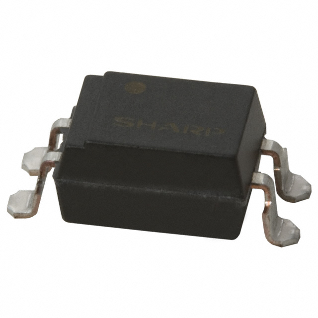
The PC3Q710NIP utilizes a 16-Mini-Flat SOIC footprint, designed with space optimization and ease of automated manufacturing in mind. This package supports high-density PCB assembly, minimizing the physical footprint while maintaining sufficient pad size for reliable solder joint formation. The compact geometry directly benefits the mechanical integration of optoelectronic components, particularly in applications where board real estate is limited or modularity is required.
Critical parameters such as lead spacing, pad layout, and package standoff height must be evaluated early in the PCB design process. The fine lead pitch facilitates tight component placement but demands meticulous solder mask definition and accurate stencil aperture design to prevent bridging or insufficient wetting during reflow. Special attention to package orientation is mandatory not only for pick-and-place accuracy but also to preserve polarity and functional alignment in signal chains.
Creepage and clearance requirements emerge as primary concerns in circuits handling high voltages, especially in isolated gate drive or signal isolation topologies. The 16-Mini-Flat SOIC package offers a separation between input and output pins that, when combined with optimized pad layouts, supports compliance with safety standards such as IEC 60664. Utilization of conformal coating or slotting on the PCB can further enhance the dielectric strength when standard package dimensions approach application limits.
Mechanical robustness during board population and field operation is augmented by the package’s well-proven SOIC form factor. The molded body and gull-wing leads absorb minor board flexure and thermal expansion mismatches. During accelerated thermal cycling or post-solder cleaning, the package’s dimensional stability and moisture resistance minimize delamination or microcracking—a frequent point of failure in alternative packages with higher standoffs or less resilient encapsulants.
From frequent board level integration, the 16-Mini-Flat variant demonstrates a reduction in solder defect rates compared to larger outline packages, particularly when using lead-free processes with tighter thermal margins. Avoiding over-constraining the leads during layout, and maintaining manufacturer-recommended land pattern dimensions, ensures that mechanical stresses do not lead to fatigue over multiple assembly cycles or prolonged operational life.
Effective deployment of the PC3Q710NIP involves not only electrical characterization but also an iterative approach to mechanical integration, emphasizing the trade-offs between package miniaturization and safety margin for insulation distances. The evolving trend toward denser, high-reliability power delivery systems underscores the continued value of well-engineered package choices that harmonize electrical performance, manufacturability, and physical durability.
Application scenarios and engineering considerations for PC3Q710NIP
The PC3Q710NIP optoisolator acts as a key component in systems requiring high-integrity galvanic isolation and robust signal transmission, notably within industrial automation and precision control architectures. In programmable logic controllers, the quad-channel architecture streamlines multi-point signal interfacing, enabling parallel data transfer and fault-tolerant redundancy across isolated domains. Motor drive circuits benefit from its fast response time and immunity to common-mode transients, facilitating precise switching and reducing noise-induced malfunctions—a common pain point in inverter-based environments. Isolated data acquisition setups leverage the device's compact integration and channel density to minimize board space while achieving reliable sampling across noisy or high-voltage sectors, an imperative in process monitoring and factory information systems.
From an engineering standpoint, signal fidelity and circuit resilience hinge on proper dimensioning of input current drivers, especially given the optoisolator’s defined forward current threshold per channel. Underestimating this parameter risks incomplete LED activation, resulting in attenuated output or logic faults; overdriving introduces long-term degradation or thermal instability. Output stage characteristics demand equal scrutiny. Load resistance and capacitance must be sized to maintain fast edge rates without ringing or overshoot, ensuring that each channel faithfully reproduces the input waveform for downstream logic or analog circuitry.
Isolation voltage stands as a critical specification, often dictated by end-system safety and regulatory frameworks such as IEC 61010 or UL 508. The PC3Q710NIP’s reinforced insulation barriers enable compliance in control cabinets operating amid high switching voltages, yet installation practices—such as PCB creepage and clearance distances—must be rigorously maintained. Field experience repeatedly underscores the importance of derating isolation parameters in environments with persistent surges, as transient overstress can silently degrade internal structures, manifesting later as unpredictable failure.
Deploying quad-channel optoisolators within multiplexed buses or high-speed sampling modules offers unique opportunities and constraints. While integrated package footprints simplify layout and channel matching, thermal loading from concurrent use across all channels must be calculated, particularly in tightly confined enclosures. Proactive thermal analysis at both board and system level prevents subtle error rate increases or early device attrition. Notably, synchronizing input timing and accommodating inter-channel skew preserve data integrity when signals traverse isolated paths with deterministic latency.
A critical yet underappreciated factor lies in board-level coupling and crosstalk mitigation. Strategic routing, ground referencing, and filter design around optoisolator banks have proven decisive in elevating system EMC performance, particularly in mixed-signal or high-impedance nodes.
The essential engineering insight for systems leveraging the PC3Q710NIP is the holistic management of device-specific electrical and physical nuances, rewarding careful interface design and thorough validation. Meticulous attention to input drive, output load match, isolation design, and layout discipline ensures the optoisolator’s functionality scales with application complexity, underpinning reliable operation in electrically hostile or safety-critical deployments.
Potential equivalent/replacement models for PC3Q710NIP
Evaluating alternatives to the Sharp Microelectronics PC3Q710NIP involves a systematic review of quad-channel optoisolators with transistor-output architectures. Key selection criteria begin at the core isolation voltage specification, where a rating of 2500Vrms ensures robust galvanic isolation for both safety and signal integrity in industrial and automation systems. Any candidate device must therefore offer precise parity on this parameter to maintain certifiable system reliability.
Beyond voltage isolation, a four-channel configuration and a compatible package outline—typically DIP-16 or surface-mount equivalents—are non-negotiable for layout retention and automated assembly workflows. This mechanical compatibility streamlines board-level substitutions, minimizing risk during production changes or dual-sourcing exercises. However, not all compatible packages guarantee electrical interchangeability. Critical attention must be paid to the input-output response time, as this directly impacts data throughput and timing margins in high-frequency control loops or multiplexed signal environments. Devices with sluggish response characteristics can inadvertently introduce control lag or data edge ambiguities, undermining system stability.
Thermal constraints demand equal scrutiny. Maximum operating temperature ratings define the upper environmental boundaries; derating curves in datasheets reveal nuanced performance behaviors under thermal stress. Optoisolators deployed in dense enclosures or proximity to heat-generating components benefit from tighter thermal margins, especially in mission-critical or extended service applications.
Datasheet comparison extends to less immediately visible characteristics such as CTR (Current Transfer Ratio) consistency, input threshold current, and leakage current in the output-off state. Even minor discrepancies can influence biasing schemes, logic compatibility, and noise immunity in edge-case scenarios. For systems exposed to strong electromagnetic disturbances, devices with robust internal shielding or enhanced surge withstand capability may outperform standard equivalents.
Practical integration frequently reveals subtle incompatibilities. For example, board-level qualification often uncovers differences in input LED forward voltage requirements or output switching profiles under load. These can be addressed with minor circuit tweaks—adjusting current-limiting resistor values or fine-tuning pull-up configurations—yet advance awareness prevents late-stage surprises.
Established brands such as Toshiba, Vishay, Everlight, and Lite-On offer quad optoisolators—like the TLP291-4, 4N35-4, or LTV-847—with overlapping performance envelopes. Testing multiple samples on site, under real application loads and clocking conditions, remains the definitive method to confirm not just datasheet compliance but also the nuanced interaction with the existing system architecture.
Viewed broadly, direct substitutions should prioritize electrical and mechanical congruence without neglecting the behavioral subtleties exposed through practical deployment. Incorporating robust validation processes at both schematic and prototype phases enables confident adoption of substitutes, supporting supply chain flexibility and long-term maintenance scalability.
Conclusion
Assessing the PC3Q710NIP optoisolator series provides insight into a device engineered for stringent requirements in high-voltage isolation and data integrity. Central to its architecture is a quad-channel format that enables simultaneous signal separation while conserving board space—an essential trait in complex industrial automation panels and densely packed power electronics assemblies. The core optical isolation mechanism, employing high-gain phototransistors, guarantees consistent switching thresholds and minimized leakage currents across each channel, directly contributing to fail-safe operation within noisy electrical environments.
The operational bandwidth and response uniformity of the PC3Q710NIP form a foundation for reliable signal transmission in pulse-width modulation schemes, digital control loops, and sensor interface circuits. These characteristics mitigate propagation delay mismatches, which, in practice, can otherwise exacerbate timing errors in synchronized multi-channel systems. The device’s transistor output topology—while straightforward—streamlines interface logic for microcontrollers and bridge drivers by offering open-collector configurations, simplifying level shifting and output aggregation strategies.
Integrating this component into system-level topologies emphasizes the importance of balancing isolation voltage ratings with transient immunity. Field observations validate that the rated isolation barrier withstands surges typical in induction motor drives, inverter stacks, or industrial I/O modules, preserving continuous signal integrity during line disturbances and ground potential disparities. Furthermore, the surface-mount footprint facilitates automated assembly and repeatable soldering quality, which directly impacts large-scale production throughput and reliability targets.
Selection strategies should extend beyond datasheet parameters, incorporating analyses of temperature derating behavior, long-term current transfer ratio stability, and compatibility with prevailing EM environments. Direct benchmarking against alternative quad-channel optoisolators reveals that the PC3Q710NIP’s competitive advantages are particularly salient where high channel density coexists with strict creepage and clearance mandates.
From a system engineering perspective, deploying the PC3Q710NIP aligns with design philosophies that prioritize modularity and maintainability. Standardizing on such an optoisolator reduces BOM complexity and streamlines firmware validation processes, especially in architectures requiring expandable or replaceable signal conditioning blocks. This approach assists in achieving regulatory compliance with safety standards such as IEC 61010 or UL 508, where documented isolation performance is mandatory.
Overall, when high-voltage isolation, channel density, and robust EMI resilience interlock as design constraints, the PC3Q710NIP series stands out as an optoelectronic interface solution that supports scalable, maintainable, and certifiable electronics platforms.