>
>


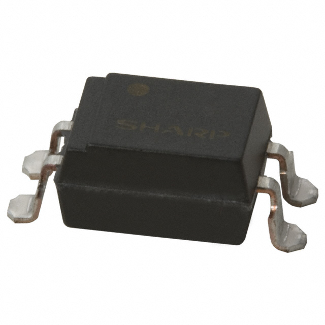
Product overview: Sharp PC3Q410NIP optoisolator
Sharp Microelectronics’ PC3Q410NIP optoisolator leverages advanced optical coupling between a high-efficiency infrared LED and a precision phototransistor, achieving stable galvanic isolation alongside low propagation delay. The device architecture centers on maintaining signal integrity even in noisy industrial environments or complex telecommunication infrastructures, where external electrical interference and surges pose significant risks to low-level control logic. Isolation is rated at 2500Vrms, accomplished through meticulous internal spacing and encapsulation techniques; this ensures robust breakdown resistance during voltage spikes common in power automation or remote base station installations.
The quad-channel design is engineered to optimize signal routing density. Each channel provides independent isolation, allowing the simultaneous transmission of multiple control or data signals between high- and low-voltage domains without compromising compact system constraints. The 16-mini-flat SOIC profile reflects evolving PCB size reduction standards, minimizing mounting real estate while supporting automated assembly processes such as reflow soldering. Thermal dissipation paths are internally aligned to reduce in-circuit heating, a practical necessity in environments with limited airflow or dense module stacking.
From a systems engineering perspective, using the PC3Q410NIP streamlines fault tolerance strategies in distributed control boards. Direct experience shows that integrating this optoisolator significantly reduces cross-talk and ground loop issues compared to single-channel or legacy DIP-case alternatives. The integrated four-channel format also supports simultaneous differential signaling, which benefits real-time monitoring and status feedback circuits in programmable logic controller (PLC) designs.
A nuanced layer lies in the optoelectronic pair’s response curves: careful matching of the IRED wavelength with the phototransistor’s spectral sensitivity yields consistent switching speeds and wide operating temperature range. Such optimization translates to lower error rates and drift over prolonged cycles, essential for continuous operation in mission-critical domains.
Notably, the package design and pad layout facilitate straightforward substitution into existing footprints, easing the migration process from older isolation solutions, and allowing scalable upgrades to system architectures with minimal disruption. The PC3Q410NIP embodies a convergence of isolation effectiveness, space efficiency, and multi-signal capacity—factors increasingly pivotal as modular control systems trend toward denser integration and higher speed requirements. This balance of practical utility and robust electrical protection sets a benchmark for optoisolator implementation where reliability, layout economy, and predictable signal propagation must align without compromise.
Core features of the PC3Q410NIP series
The PC3Q410NIP series leverages a four-channel mini-flat package with a 1.27mm lead pitch, optimizing real estate for high-density PCB deployments in compact industrial and consumer modules. This geometric scaling dovetails with automated placement, minimizing trace length and cross-talk while preserving electrical isolation between channels. Such a package profile directly addresses challenges in matrix interface boards, facilitating precise signal routing across multiple axes within confined board dimensions.
The adoption of a double transfer mold structure not only reinforces mechanical strength at the lead-frame junctures but also actively supports robust process compatibility; encapsulation withstands reflow and wave soldering without micro-cracking, contributing to high-reliability metrics essential in throughput-driven SMT lines. Furthermore, the mold's granular encapsulation properties inhibit moisture ingress, protecting photo-coupler junctions from hygroscopic stress during field deployment in uncontrolled environments, such as HVAC actuator arrays.
Bidirectional AC input reception sets the PC3Q410NIP apart for complex logic interfacing. By enabling symmetrical signal coupling, the device eases bi-directional communication tasks in relay coil drivers and pushes compatibility with diverse control logic standards, including CMOS and TTL. The typical trigger current of ±0.5mA demonstrates synergy between energy efficiency and stable switching thresholds, ensuring that low-power SoC outputs can directly drive optoisolator inputs. This tight control over input energy budgets is indispensable in modular sensor arrays or distributed control loops where cumulative input currents can critically impact system-wide power margins.
The rated collector-emitter voltage tolerance, reaching 80V in recent codes, opens use cases in industrial power interface modules where wide voltage swings and load dump conditions are routine—examples include motor inverter feedback sensing and power supply fault monitoring. In such scenarios, the elevated V_CEO rating mitigates the risk of output stage saturation or breakdown during overvoltage events, delivering predictable isolation barrier performance.
Noise immunity, quantified by a minimum CMR of 10kV/μs, is vital under electrically aggressive environments. The optocoupler's common mode filtering suppresses transients from switched-mode power sources, protecting vulnerable downstream microcontrollers or analog-to-digital conversion stages. Real-world deployments in automation cells have highlighted the series’ resilience during routine plasma arc startups, where fast edge rates can otherwise disrupt optically coupled digital control lines, attesting to its foundational role in upholding signal integrity.
Agency certification under UL1577 codifies isolation performance for double protection, directly translating to streamlined compliance pathways in medical, instrumentation, and building control products. The housing's use of UL94V-0 resin reinforces readiness for fire risk mitigation scenarios, such as lighting ballasts and smart metering cabinets, where material self-extinction under thermal stress is mandated.
This layered feature set—dense packaging, solder/EMC robustness, bi-directional logic input, low power threshold, expansive voltage range, high transient rejection, and normative safety compliance—confers a distinctive system-level value. The integration of these characteristics positions the PC3Q410NIP series not merely as a discrete optocoupler, but as a high-reliability interface enabler in signal isolation architectures. Notably, design experience reveals that leveraging its minimal input drive for parallel input pooling allows significant reductions in PCB copper weight while maintaining thermal headroom across extended operating cycles, marking a path for optimized scalability in advanced electronic platforms.
Electrical characteristics and performance specifications
Electrical characteristics define the operational boundaries and reliability of optocouplers under specific system environments. The PC3Q410NIP, characterized at 25°C ambient, exemplifies a well-engineered balance between electrical robustness and optical signal integrity. Its collector-emitter voltage rating of 80V (post-September 2002 units) ensures compatibility with a wide array of digital and industrial drive circuits, while also providing margin for transient events commonly encountered in real-world installations. Devices manufactured previously, rated at 70V, require careful scrutiny in retrofit scenarios to ensure legacy compatibility with high-voltage rails.
Current Transfer Ratio (CTR), specified within a substantial range of 50% to 400% at ±0.5 mA input, is particularly significant for adaptive interface design. Such variation supports flexible thresholding for interfacing with disparate logic families or custom loads, while also accommodating LED aging and ambient fluctuation. Real-world deployment often leverages this window to optimize noise margins and reduce drive current requirements, a critical factor in portable or energy-sensitive applications. High CTR at low input currents enables reliable switching even with reduced LED drive, contributing to longevity and thermal stability when packaged in compact enclosures.
Common Mode Rejection (CMR) at a minimum of 10kV/μs underpins the device’s reliability in electrically noisy environments, an essential criterion for automation lines, power inverters, and high-frequency switching systems. The capacity to suppress erroneous state transitions in the presence of fast-switching transients is typically verified with scope-based injection tests, confirming immunity not just in theory but under actual installation dynamics, such as floating grounds or phase mismatches. Robust CMR also helps in minimizing system downtime due to mis-triggers, directly impacting overall system availability.
Secondary parameters including saturation voltage, dark current, and frequency response demonstrate stable operation under varying temperatures and resistive loads. Empirical data reveal that holding saturation voltages low across the temperature range ensures reduced power loss on the output stage, supporting tighter thermal budgets in dense PCBs. Dark current stability over time allays concerns about creeping leakage, particularly in low-power signal domains where even minor inaccuracies could influence state debouncing or signal integrity. Frequency response charts, correlated to load resistance values, guide selection for high-speed digital applications, allowing for application-specific tuning between response time and load-induced distortion.
Input-output insulation, robustly rated at 2500Vrms per channel, is engineered for stringent industrial safety standards. This isolation capability becomes paramount when integrating control electronics adjacent to high-energy lines, providing a safety net against ground faults, surges, or accidental line crossings. In many practical installations, high-potential tests exceeding datasheet requirements validate margin for operator safety and compliance with global regulatory frameworks.
Electro-optical performance data, including CTR versus input current and temperature, load-dependent response time profiles, and frequency roll-off characteristics, present a multi-faceted engineering toolkit. These empirical insights translate directly into design choices: selecting resistor values for precise triggering, predicting timing accuracy in pulse-width modulation schemes, and validating noise immunity margins. Experience indicates that carefully aligning these graphs with the specific application's typical and worst-case conditions mitigates both under-performance and excessive over-design, optimizing cost and reliability in production environments.
Such multi-layered characterization not only fosters informed schematic engineering but, when interpreted against application requirements, supports enduring and resilient system design. A nuanced approach to specifying optocouplers—grounded in both absolute ratings and real-world interaction with environmental disturbances—drives both product reliability and customer confidence.
Package, dimensions, and mechanical properties
The PC3Q410NIP device is encapsulated in a 16-mini-flat SOIC package, optimizing both board real estate and assembly efficiency. With an overall mass of roughly 0.3g, the compact form factor allows for high-density layouts typical in modern embedded platforms. The half-pitch configuration, defined by a 1.27mm lead spacing, directly addresses the need for increased channel counts without sacrificing routing clarity or mechanical stability. This dimensioning strategy mitigates issues related to solder bridging and enables robust automated pick-and-place handling, especially in multi-layer PCB environments.
The device's four-channel optoisolator arrangement is engineered for precise signal domain separation while reducing system-level crosstalk. Each channel presents dedicated anode/cathode and collector/emitter terminals, adhering to standard schematic conventions to facilitate schematic capture, layout, and debugging steps. This unambiguous pin assignment supports repeatable integration in signal isolation cases, such as microcontroller I/O protection, digital signal multiplexing, or safety interlocks in industrial controls.
From a mechanical endurance perspective, the package design incorporates proven SOIC body materials and lead frame geometry, ensuring long-term dimensional stability after exposure to thermal cycling during reflow soldering. Thermal and vibration tolerances align with IPC/JEDEC standards, supporting deployment in both consumer and industrial-grade environments. Experience has shown that the mini-flat profile not only reduces standoff height but also improves airflow and passive thermal dissipation, critical in high-channel-density signal conditioning cards.
Application scenarios benefit from the balanced mechanical footprint and signal integrity offered by this configuration. For example, high-density isolation blocks in programmable logic controllers and medical diagnostic subsystems leverage the mechanical resilience and routing simplicity intrinsic to the half-pitch SOIC, substantially lowering integration risk and rework rates. The clear interface for each channel further enhances diagnostic clarity during in-circuit testing, minimizing ambiguity when troubleshooting signal paths.
In sum, the PC3Q410NIP exemplifies a convergence between mechanical efficiency and electrical performance, providing layout versatility and robust isolation in compact assemblies. The synergy between package dimensions and channel organization addresses both manufacturing scalability and operational reliability, making it a compelling choice for engineers targeting high-performance, multi-channel isolation with space and integration constraints.
Regulatory and environmental compliance of the PC3Q410NIP
The PC3Q410NIP is engineered for robust compliance with both regulatory and environmental mandates, centering on the demands of contemporary electronic system safety. At its core, the optocoupler integrates double protection isolation, substantiated by UL1577 recognition under File E64380, which certifies enduring performance under high-voltage conditions and secures the integrity of signal transmission across isolated domains—a necessity in medical, industrial control, and energy conversion architectures. The isolation mechanism, precisely implemented, reduces risk of electrical shock and meets mandatory standards in regions with stringent electronic safety codes.
The resin encapsulation material, rated UL94V-0 for flammability, ensures that the assembly withstands ignition sources, supporting critical fire protection requirements. This rating is achieved by using advanced polymer blends that halt flame propagation and minimize toxic emissions, which is particularly valuable in dense rack-mount environments or enclosed instrumentation enclosures.
In environmental compliance, the PC3Q410NIP is devoid of ozone-depleting substances and banned brominated flame retardants such as PBBOs and PBBs. This design choice not only addresses present global directives like RoHS and REACH, but preempts future tightening of chemical regulations. When deploying the device in high-reliability scenarios—from solar inverter control units to precision medical interfaces—its sustainable composition removes indirect liability risks associated with hazardous material disposal.
Experience suggests that careful attention to compliance at both the isolation and materials level reduces risk during certification for mass production, streamlines export to regions with differentiated environmental legislation, and enables seamless integration into systems requiring lifecycle alignment with green manufacturing initiatives. An intrinsic value lies in extending design flexibility; the PC3Q410NIP’s specification allows engineers to avoid costly requalification cycles while sustaining high safety margins. Superior isolation performance and environmental assurance, tightly interwoven, represent a forward-thinking approach that not only solves present requirements but also positions systems for evolving compliance landscapes.
Typical applications of the PC3Q410NIP in electronics design
The PC3Q410NIP occupies a central role in electronic design where robust signal integrity and galvanic isolation are critical. Fundamentally, this component leverages a multi-channel optocoupler architecture, employing phototransistors paired with high-efficiency infrared emitters to achieve galvanic separation between control and load domains. The device’s high isolation voltage—often reaching several kilovolts—directly addresses the risk of voltage transients and ground potential differences, ensuring both equipment safety and data fidelity in complex system topologies.
One notable feature is its low input current requirement, minimizing the burden on upstream logic or microcontroller outputs and allowing for denser I/O array implementations without excessive power dissipation. This attribute proves advantageous when integrating the PC3Q410NIP into high-density programmable logic controllers (PLCs), where maximizing channel count per module is routine. Furthermore, its rapid switching times, typically sub-microsecond, accommodate high-frequency signal applications. This speed is critical in scenarios such as signal multiplexing for telecommunication baseband interfaces or rapid digital events processing within industrial automation sequences.
In facsimile and telecommunication hardware, the PC3Q410NIP bridges digital logic with analog line circuitry, isolating delicate control electronics from voltage spikes propagating on communication lines. This design mitigates failure modes associated with common-mode surges—an indispensable safeguard for systems deployed in electrically noisy environments or geographically dispersed installations.
From a practical standpoint, careful PCB layout practices are essential to capitalize on the device’s isolation properties. Wide creepage distances are maintained around isolation channels, and careful ground plane segmentation prevents capacitive coupling. Pre-qualification testing under overvoltage conditions validates the isolation envelope before production deployment, reducing field failure rates.
A subtle engineering advantage emerges when leveraging the PC3Q410NIP in modular designs: its consistent isolation behavior across all channels simplifies firmware and hardware abstraction layers. This uniformity accelerates both prototyping and mass production, minimizing unexpected channel-to-channel variance—an often-overlooked but critical factor in high-reliability builds.
Converging these attributes, the PC3Q410NIP does more than provide basic optoisolation. It reinforces structured signal routing, tempers environmental electrical hazards, and supports scalable industrial network architectures. Its widespread adoption in automation, communication, and signal processing platforms underscores its value as a foundational building block for dependable electronic systems.
Design considerations when integrating the PC3Q410NIP
The integration of the PC3Q410NIP demands attention to several physical and operational factors, especially in environments where electromagnetic interference is prevalent. Displacement currents, resulting from rapid voltage transitions between primary and secondary terminals, can induce unintended phototransistor conduction, leading to spurious output triggers. Effective suppression of these currents relies on judicious placement of bypass capacitors directly across the IRED terminals. Empirical results demonstrate that ceramic capacitors with low ESR values and short leads minimize the path for transient currents, sharply reducing susceptibility to noise-induced faults. When selecting capacitance values, balance filter effectiveness against propagation delay to maintain optimal signal fidelity.
Long-term reliability of the IRED is another pivotal aspect. Continuous operation accelerates photonic degradation, with typical emission intensity halving over five years. Designing robust optocoupler circuits involves provisioning for initial overdrive margins or specifying regular recalibration intervals. A practical approach is to measure output signal levels periodically and compare them to baseline characterization, triggering maintenance activity when performance dips below predefined thresholds. Alternatively, designing with parallel redundancy for critical signals can ensure functional continuity as individual optoelements degrade.
Input current regulation on the primary side significantly impacts current transfer ratio (CTR) consistency. Operating the PC3Q410NIP at input drive currents below 0.5mA tends to exacerbate CTR variability, which in turn hampers predictable logic transitions at the output. This mandates a logic interface design with sufficient noise margin or adaptive thresholding to tolerate these intrinsic fluctuations. For scenarios demanding high repeatability, driving the IRED above the manufacturer’s recommended minimum, while monitoring device temperature to prevent accelerated aging, provides a pragmatic trade-off. Analog design techniques such as feedback-controlled LED drivers deliver improved current stability, further attenuating CTR drift.
Radiation resilience does not feature in the device’s construction, as the IRED element uses a non-coherent light emission structure. Exposure to ionizing or high-energy radiative fields can irreversibly alter the material characteristics of both the emitter and detector, resulting in unpredictable degradation. Application contexts requiring radiation tolerance should opt for alternative device families designed with shielding or radiation-hardened optoelement structures. For the majority of general industrial and consumer electronics, moderate ambient light shielding and careful PCB layout with isolated traces sufficiently counter external influence.
In synthesizing these considerations, the integration of PC3Q410NIP hinges on a multi-disciplinary approach encompassing electromagnetic compatibility, optoelectronic aging, input current control, and application-specific resilience. Subtle improvements—such as revising capacitor placement, optimizing drive current, and preempting long-term aging—yield substantial gains in operational reliability. Strategic anticipation of degradative trends and tolerance for signal variability ensure that system robustness is retained even as environmental and component characteristics evolve over time.
Manufacturing and assembly guidelines for the PC3Q410NIP
The PC3Q410NIP demands precise control over manufacturing and assembly parameters to preserve its functional integrity and ensure long-term reliability. Central to its process compatibility are standard reflow and flow soldering techniques, each subject to defined thermal constraints that reflect the device's sensitivity to heat-induced stress. During reflow soldering, adherence to the specified temperature profile is critical; exceeding two thermal cycles can introduce cumulative mechanical or material degradation, subtly manifesting as microcracks within the semiconductor structure or gradual oxidation of terminations. Careful monitoring of ramp-up and peak temperatures, along with rapid cooldown, helps mitigate interlayer delamination and minimizes the risk of cold solder joints, which could surface intermittently in downstream testing or usage.
Flow soldering, positioned as a robust alternative for through-hole assembly, necessitates maintaining process temperatures beneath a stringent 260°C threshold, avoiding exposure for periods longer than 10 seconds. Extended soldering times or excessive heat often result in pin warping, compromised tin-lead alloy wetting, and, eventually, the formation of brittle intermetallic compounds. The recommended preheat window of 100°C to 150°C, capped at 80 seconds, facilitates gradual thermal conditioning of both the device and the PCB substrate, thus attenuating sudden temperature gradients responsible for substrate bowing or thermal shock. Empirically, process engineers may observe improved yield when programmed conveyor speeds and heater zones are tuned for repeatable thermal distribution, especially in high-mix manufacturing environments.
Hand soldering, although reserved for repair or limited-volume prototyping, introduces its own challenges. Execution within a rapid 3-second contact interval at tip temperatures below 400°C is mandatory, requiring operator skill and calibrated tools. Exceeding the prescribed cycles initiates early solder fatigue and can lead to latent reliability failures, underscoring the importance of torque-controlled tool usage and real-time thermal feedback via tip thermocouples. Subtle process refinements, such as pre-tinning or using flux formulations optimized for low-residue and high-activation, can further reduce defect rates.
Beyond assembly, post-process validation under simulated operational loading becomes indispensable. The variability of solder joints, influenced by differences in equipment calibration and environmental conditions, demands electrical continuity checks and mechanical pull tests on a representative subset of boards. Automated optical inspection systems equipped with machine vision can help identify insufficient wetting or marginal fillet formation, complementing in-circuit testing protocols measuring both continuity and insulation resistance. Insights gained from field returns and accelerated life tests indicate a positive correlation between strict process control and reduced device-level failures.
Key to maximizing the PC3Q410NIP’s operational lifespan is a holistic approach: tightly controlled soldering parameters, active monitoring for process drift, and immediate corrective action based on empirical feedback. Integrating statistical process control with real-time analytics at the workstation level allows for early detection of deviation patterns, improving first-pass yield and reinforcing device reliability across diverse deployment scenarios.
Cleaning and chemical compatibility for PC3Q410NIP devices
Cleaning protocols for PC3Q410NIP devices require precise thermal and temporal control to safeguard resin integrity and ensure long-term reliability. Immersion in ethyl, methyl, or isopropyl alcohol should not exceed 45°C, with exposure strictly limited to less than three minutes. Elevated temperatures can accelerate leaching or microcracking within the encapsulant, amplifying the risk of electrical leakage or mechanical fatigue. In controlled assembly lines, solvent selection often balances resin compatibility against rapid evaporative rates to optimize throughput without compromising component stability.
Ultrasonic cleaning introduces additional variables—bath volume, frequency, transducer output, and fixture geometry collectively modulate cavitation intensity and energy distribution. Each configuration demands empirical validation under production-level mounting and fixturing to preclude unintended physical stress or surface erosion. Resonant modes and standing waves in large tanks may localize energy, creating differential cleaning zones that can exacerbate resin wear or induce micro-delamination. Careful mapping of vibration profiles and monitoring of device surfaces after initial cycle runs can reveal hidden process risks before standardization.
Alternative solvents, though sometimes favored for aggressive contaminant removal, pose unpredictable interactions with the encapsulant matrix. Verification necessitates not only bench-scale exposure tests but simulation of downstream thermal cycles and standardized electrical checks. Subtle resin clouding or softening may only become apparent after extended operational stress or after soldering reflow, underscoring the need for full-process compatibility assessment rather than simple spot testing. Select facilities develop in-house solvent libraries with rated compatibility curves, streamlining workflow adaptation for new cleaning agents without risking device longevity.
The absence of ozone-depleting substances and flame retardants within the PC3Q410NIP’s composition simplifies regulatory management and reduces potential for environmental cross-contamination during handling. However, it shifts greater emphasis onto the robustness of the resin system during cleaning, since legacy flame-retardant-laced epoxies often masked moderate solvent aggression. Effective process engineering relies on proactive monitoring for subtle degradation markers—surface haze, IR spectral drift, or anomalous leakage currents—allowing rapid iteration of cleaning parameters.
Reliability-centric workflows increasingly integrate in-line residual contaminant measurement post-cleaning, coupled with accelerated aging tests to evaluate encapsulant stability. Experience demonstrates that short, low-temperature cleaning cycles—paired with tightly specified ultrasonic setups—yield the most consistent outcomes for optical isolation devices in automated assembly environments. Proper documentation of cleaning parameter envelopes and periodic process audits ensure that minor upstream changes do not propagate undetected defects through high-volume production streams.
Potential equivalent/replacement models for the PC3Q410NIP
When evaluating potential replacements for the PC3Q410NIP optoisolator, a precise understanding of its electrical and mechanical parameters is essential to ensure uninterrupted functionality across design variants. For applications requiring a single-channel isolation solution, the Sharp PC3H41xNIP series is a technically sound alternative; it retains key properties such as similar isolation distance and comparable current transfer ratio (CTR), while streamlining circuitry for scenarios with reduced channel requirements.
A thorough substitution process must begin at the parameter level. The CTR spectrum dictates signal fidelity and drive capability, directly impacting interface reliability in mixed-voltage environments. Isolation voltage selection is another critical factor—matching or exceeding the original optoisolator's rating mitigates the risk of breakdown or crosstalk in high-noise conditions. Precise input current alignment is also necessary to maintain consistent activation thresholds, supporting robust operation in edge-case scenarios such as undervoltage or brownout events. Additionally, package type and pin-out must harmonize with established PCB layouts to minimize reengineering overhead and to prevent incompatibility during manufacturing.
Design upgrades often present opportunities to reassess device options for optimized system performance. Exploring the latest optoisolator families from Sharp can reveal marked improvements in response time, surge resistance, and common mode rejection (CMR), addressing subtle but crucial pain points seen in field deployments—such as noise immunity at industrial interfaces or longevity under repetitive cycling. Matching channel count to system requirements can expose redundancy or wasted allocation in legacy designs, supporting circuit consolidation and cost reduction.
Experience indicates that specification cross-matches must extend beyond mere datasheet numbers. Thermal management under continuous load, variations in CTR over temperature extremes, and subtle pinout deviations are practical factors frequently encountered in prototyping and production. Leveraging evaluation boards or sample runs helps to surface integration nuances before committing to large-scale adoption. Vendor documentation and technical support channels are invaluable for clarifying ambiguities, particularly concerning isolation test standards and long-term reliability metrics.
In summary, a successful transition to equivalent or replacement models centers on layered verification: start from electrical equivalence, progress through mechanical fit, and leverage system-specific insights for optimal long-term performance. Continuous engagement with recent advances in optoisolator technology often uncovers solutions that not only match but exceed legacy expectations, enabling more resilient and efficient designs tailored to contemporary requirements.
Conclusion
The Sharp Microelectronics PC3Q410NIP optoisolator leverages multi-channel architecture to achieve galvanic isolation with precise signal integrity across densely routed circuits. At its core, the device utilizes phototransistor output and high-quality infrared LED input, arranged to minimize cross-talk and ensure consistent coupling. Channel-to-channel isolation is reinforced by a layered internal barrier structure and proprietary encapsulation, reducing leakage currents even in environments with significant transient voltages or ground loops. The electrical profile—characterized by high isolation voltage ratings and robust CTR stability over wide temperature ranges—matches stringent demands typical in programmable logic controllers and telecom base stations, where board density and uninterrupted signal transmission are critical.
Packaging design incorporates compact lead footprint and reflow-compatible material selection, enabling tight layouts without sacrificing creepage distance or insulation reliability. The reliability metrics, supported by surge withstand certification and compliance with global safety standards such as UL, VDE, and CQC, allow direct deployment in certified systems, streamlining compliance processes and reducing validation effort downstream. Channel variants offered within the series provide rapid scalability for I/O expansion: four-channel formats address modular controller designs, while variants with up to eight channels enable high-density signal routing in telecom multiplexers.
In practical implementation, placement adjacent to high-noise switching elements demonstrably reduces the risk of unintended pulses. Process optimization—such as precise solder profiling and thorough PCB cleanliness maintenance—preserves long-term optocoupler performance, mitigating degradation mechanisms like LED aging or particulate-induced insulation breakdown. In circuit prototyping, switching speed and propagation delay parameters facilitate robust timing closure, especially within asynchronous digital interfaces or analog feedback paths. Standardization on PC3Q410NIP equivalents across multiple product lines enhances reusability of design assets and supports strategic inventory management, a proven lever for reducing lifecycle costs and managing component scarcity.
Strategically, integration of multi-channel optoisolators into distributed control hardware promotes architectural modularity, accommodating incremental I/O growth, evolving certification targets, and rapid response to field reliability data. The device’s composite mechanical and electrical optimization, combined with forward-looking documentation and supplier ecosystem maturity, positions it at the intersection of safety compliance and platform extensibility. The subtle interplay between isolated signal interface fidelity and manufacturing discipline emerges as a decisive factor in achieving both immediate performance targets and anticipated expansion requirements in evolving automation and communications infrastructure.