>
>


Product overview of Sharp PC357N2 optoisolator
The Sharp PC357N2 optoisolator operates as a single-channel optical isolator integrating a high-efficiency infrared LED and a phototransistor within a compact package. The principal mechanism centers on converting an electrical input signal into modulated infrared light, subsequently detected by the integrated transistor. This conversion process achieves galvanic isolation between input and output sides, effectively blocking unwanted current transfer, transients, or noise. Isolation voltage ratings typically exceed 3750 V(rms), ensuring compliance with demanding safety and reinforced insulation requirements in industrial domains.
Internally, the structure exploits the linear response of the phototransistor to varying LED current, enabling precise control of ON/OFF switching or analog signal transmission in low to moderate frequency bands. The coupling factor and CTR (Current Transfer Ratio) are optimized for stable operation across supply fluctuations and ambient temperature variations, aiding consistent performance in high-noise environments such as switch-mode power supplies, motor drives, and PLC systems. The device’s low-profile SOP4 package is engineered for automated placement and space-constrained designs, streamlining assembly across both high-volume and specialty manufacturing lines.
Application versatility is highlighted through its use in microcontroller I/O isolation, where bidirectional data path integrity is critical against ground loops or voltage transients. In switched power domains, it enables reliable feedback or sequencing while maintaining safety boundaries between high-voltage and logic circuits. The device’s predictable switching characteristics and low input drive requirements facilitate seamless interface with digital control boards, where throughput, board density, and power efficiency are prioritized.
Reliability under continuous operation is underpinned by optimized semiconductor fabrication processes and robust mechanical encapsulation. Experience demonstrates the PC357N2’s resilience in environments subjected to frequent switching, variable input voltages, or thermal stress—factors commonly encountered in industrial relay interface, sensor acquisition, or telemetry nodes. The sharply defined isolation margin significantly reduces fault propagation risks, supporting system-level certification under IEC, UL, or similar standards.
A noteworthy insight pertains to design scalability: the device’s balance of electrical performance with manufacturability allows for straightforward migration, whether upscaling to multi-channel architectures or adapting to evolving safety regulations. In iterative development cycles, its repeatable performance and predictable aging characteristics offer confidence in long-term system planning and lifecycle management. Incorporated within well-engineered layouts, the PC357N2 functions as a critical enabler for robust modular isolation, forming the backbone of modern signal interface strategies.
Key technical features of Sharp PC357N2 optoisolator
The Sharp PC357N2 optoisolator is engineered to achieve robust galvanic isolation through optical coupling, preventing direct electrical paths between input and output circuitry. Internally, the mechanism relies on an infrared LED, which emits light in response to input signals. This light interacts with a phototransistor on the output side, transducing the optical signal back to an electrical form. The transistor output configuration facilitates swift switching responses, highly compatible with CMOS and TTL logic levels, reducing propagation delays and enabling reliable digital signal interfacing across isolation boundaries.
One of its most critical metrics is the 3,750 Vrms isolation voltage. This value quantifies the device's capacity to withstand substantial potential differences between high- and low-voltage domains without breakdown, an attribute vital for industrial automation, medical instrumentation, and power supply feedback loops. Designers often leverage this specification when segregating control logic from hazardous voltages within power conversion systems or motor drives, mitigating risks of ground loops and unintended conduction.
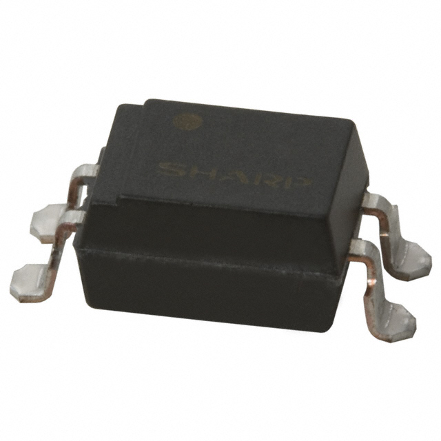
The PC357N2’s 4-mini-flat encapsulation presents a notable advantage for compact PCB layouts. The reduced footprint streamlines high-density board assembly and optimizes thermal management via shorter thermal paths. Compatibility with standard reflow soldering processes further minimizes manufacturing complexity, enabling volume production with consistent attachment reliability. This package form factor also enhances insertion rates during automated pick-and-place operations, reducing cycle times in SMT lines.
An additional layer of resilience is evident in its electrical noise immunity. Noise transients—arising from nearby switching loads or electrostatic discharges—are a perennial challenge, especially in data acquisition modules and communication interfaces. By coupling signals optically, the PC357N2 inherently disrupts the conduction of common-mode noise, preserving signal fidelity even in electrically turbulent environments. Such behavior can be observed in precision sensor amplifiers, where output stability is preserved despite aggressive environmental fluctuations. The optoisolator’s performance under such scenarios often surpasses alternatives relying solely on passive filtering or shielding.
A best practice observed in deployment involves optimizing load resistance on the transistor side, fine-tuning response speed against output voltage swing needs. Close attention to PCB trace layout, avoiding parallel runs with high-current paths, further capitalizes on the optoisolator’s isolation and noise-blocking features. Notably, the convergence of small form factor, high isolation, and swift digital compatibility enables modular architectures in distributed control systems—facilitating maintenance, scalability, and field upgrades.
The central insight here lies in recognizing that the optoisolator is not merely a safety element but a key enabler of system robustness and flexibility. Leveraging its technical nuances—from signal integrity to process integration—designers create architectures that scale in both complexity and reliability, meeting evolving industry standards for electromagnetic compatibility and functional safety.
Electrical and isolation performance of Sharp PC357N2 optoisolator
The Sharp PC357N2 optoisolator is engineered to provide robust galvanic isolation, utilizing an internal LED-phototransistor pair to transfer signals across an electrically isolated barrier. This topology achieves a certified isolation voltage of up to 3,750 Vrms, a performance threshold validated through high-pressure insulation and partial discharge tests. Such isolation metrics are critical for safeguarding low-voltage domains from switching transients, ground loops, and overvoltage events that commonly occur in industrial and power-conversion contexts.
The output configuration of the PC357N2, based on a phototransistor, enables low propagation delay and signal fidelity. The response speed and linearity of the phototransistor stage ensure compatibility with legacy TTL and modern CMOS logic inputs, a key consideration when integrating into signal chains that demand both noise immunity and timing precision. In practice, the open-collector output allows flexible integration, supporting active pull-up designs and even wired-OR topologies without modification to the optocoupler itself.
Design parameters are calibrated for streamlined single-channel deployment, simplifying layout requirements in isolated feedback paths for switch-mode power supplies, digital control loops, and communication interfaces. The physical package provides clearances and creepage distances compliant with international safety standards, reducing the burden on PCB designers to compensate for isolation deficiencies through elaborate layout techniques or costly supplementary insulation.
Long-term testing protocols, including aging under bias and thermal cycling, confirm that the PC357N2 remains stable across a wide range of drift and temperature conditions. Such reliability is indispensable where continuous operation must coexist with exposure to electrical stress or environmental variations. Consistency across phototransistor CTR (current transfer ratio) bins further alleviates the need for post-assembly calibration, supporting mass production targets of yield and repeatability.
While the PC357N2’s architecture favors robustness and ease of integration, its single-channel configuration also encourages modular isolation strategies. Designers addressing complex systems can decompose isolation challenges into manageable segments, selectively allocating optoisolators in high-risk nodes without proliferating part diversity or introducing interface ambiguities.
Current trends in safety-critical automation and compact power electronics highlight the competitive need for optoisolators balancing isolation integrity and interface compatibility. The PC357N2 exemplifies a design discipline centered on insulation performance without sacrificing signal throughput or board-level simplicity. Deployment in environments characterized by fluctuating ground potentials or EMI underscores the importance of component-level isolation as a first line of defense, enabling more systemic resilience and long-term field reliability.
Package and implementation considerations for Sharp PC357N2 optoisolator
The Sharp PC357N2 optoisolator leverages a 4-mini-flat package that directly addresses PCB space constraints in contemporary electronic design. The minimized package geometry translates to efficient layout practices, facilitating tight component placement within high-density circuits. This compact form factor is particularly advantageous in scenarios demanding extensive channel isolation, such as multi-layered signal processing boards where proximity constraints define system reliability and electromagnetic compatibility.
Electromechanical integration benefits stem from the package’s suitability for automated surface-mount assembly. The flat leads and shallow body enable predictable reflow soldering profiles, reducing the likelihood of cold joints and tombstoning during mass production. This harmonizes with modular manufacturing systems that rely on rapid throughput and standardized mounting. The repeatable assembly outcome directly influences defect rates and long-term mechanical stability, fostering higher overall yield and predictable performance in volume production environments.
The single-channel nature of the PC357N2 presents inherent scalability, simplifying incremental design modifications. This modularity is effectively exploited in distributed architectures that require per-channel isolation, such as industrial control interfaces and sensor arrays. By deploying discrete optoisolators, designers can tailor isolation protocols without over-committing to unnecessary complexity or channel redundancy. This approach enables precise allocation of isolation boundaries based on risk assessment, protecting sensitive nodes while optimizing resource utilization.
Thermal management considerations must not be overlooked; the mini-flat package assists heat dissipation through low-profile contact with the PCB, enabling more efficient conduction paths than taller through-hole alternatives. Empirical layout approaches often leverage increased copper fill under and around each optoisolator, integrating thermal vias beneath the thermal pad footprint to further mitigate localized heating. This is critical in systems exposed to fluctuating ambient conditions and variable load profiles, where optoisolator longevity and signal integrity must be maintained.
From a board-level signal integrity perspective, the reduced footprint allows designers to minimize parasitic capacitance and inductance in high-speed or sensitive circuits. Placing the PC357N2 closer to the signal source supports lower propagation delay and preserves critical timing margins. Iterative design validation frequently uncovers improved noise immunity when isolation components are positioned using such compact packages, reinforcing the utility of the mini-flat format in robust signal isolation environments.
Strategically, opting for scalable single-channel isolation devices like the PC357N2 allows future system expansion and modular upgrades without redesigning the base layout. This architectural foresight benefits maintainability and long-term cost control, as additional isolation channels can be integrated on demand. The flexibility of the packaging, combined with the proven mechanical reliability achieved in prototyping and production runs, demonstrates the synergy between package design and practical engineering requirements. By focusing on these multidimensional implementation aspects, optimized optoisolator selection and layout become integral to achieving resilient, high-density electronic systems.
Potential equivalent/replacement models for Sharp PC357N2 optoisolator
Sharp PC357N2 optoisolators, characterized by their transistor-output configuration and compact DIP or SOP packaging, are widely used for galvanic isolation in low- and medium-voltage applications. When sourcing becomes challenging or design pivots require alternates, the search for equivalent or replacement devices must be anchored in a nuanced understanding of both electrical and physical parameters.
At the foundational level, the primary function is bidirectional electrical isolation while ensuring signal integrity between control and power circuitry. Any substitute device must therefore provide comparable input-to-output isolation voltage—typically 3750 Vrms or higher—to uphold safety margins. Output configuration is equally critical: a phototransistor output with similar current transfer ratios (CTR), ideally within the 50-600% range under specified test conditions, ensures drop-in compatibility and predictable response. Matching the package’s footprint and pinout preserves PCB layout and assembly flows, reducing engineering overhead and revalidation time.
Beyond datasheet parity, a deeper vetting of performance variables becomes vital. Switching speed—commonly within 3–10 μs for PC357N2-class parts—can subtly affect control loop timing or high-frequency pulse fidelity, especially in precision feedback or zero-cross detection circuits. Devices with markedly slower response may introduce latency, while excessively fast types might accentuate noise coupling if board layout lacks adequate filtering. Robustness across environmental extremes and long-term aging must also factor into the evaluation. Variations in CTR drift, especially under high temperatures or after extended operational hours, can erode system reliability. Manufacturers with mature process controls and demonstrable field performance often deliver tighter lot-to-lot tolerances, reducing post-production calibration effort. In high-volume deployments, tighter CTR bins combined with stable switching thresholds smooth production test and tuning, ultimately streamlining throughput.
Application-specific requirements may further steer substitution choices. For motor controller designs or industrial PLCs operating amidst electrical transients, parts with reinforced insulation and UL or VDE safety ratings confer regulatory headroom. In consumer electronics, footprint minimization can prioritize SO-4 or Mini-Flat packages, making newer equivalents from Vishay, Toshiba, ON Semiconductor, or Lite-On especially attractive. It is prudent to review application notes and cross-reference sheets from these vendors to verify subtle idiosyncrasies—such as pulldown resistor requirements or collector-emitter saturation voltage—do not conflict with legacy designs.
First-hand integration projects reveal the strategic value of bench-testing sample lots of candidate replacements under representative stress: multiple temperature cycles, variable VCE loads, and high/low CTR bins expose edge performance and mitigate surprises during ramp. Often, redesigning for optoisolators with slightly superior CTR stability, even at a modestly higher cost, can prevent elusive field failures and reduce long-term warranty risk. Ultimately, systematic cross-evaluation—balancing datasheet conformance, application fit, and supplier reliability—enables cost-effective continuity in both legacy and forward-looking optoisolated designs.
Conclusion
The Sharp PC357N2 optoisolator presents a compelling set of attributes for signal isolation in compact electronic assemblies. Its architecture combines a phototransistor output stage with an optimized input LED configuration, enabling the device to achieve reliable electrical separation between critical subsystems. The optically coupled interface supports high isolation voltage levels, typically rated at 3750 Vrms, which mitigates risks associated with transient surges and ground potential differences across complex circuit topologies.
At the fundamental level, the PC357N2 leverages a monolithic housing design to minimize board space and streamline PCB layout challenges. The package not only conserves area in high-density designs but also constrains parasitics that can degrade signal integrity in sensitive control circuits. The efficient current transfer ratio translates into consistent switching behavior and predictable signal propagation delays, allowing precise timing management in digital interfaces such as microcontroller inputs, relay drivers, or industrial PLC systems. Designers working within stringent space and performance envelopes benefit from the device’s pin compatibility and straightforward integration with existing footprints, reducing iterative prototyping cycles.
When embedding the PC357N2 within galvanic isolation barriers, attention to input LED drive parameters and collector-emitter load conditions enables engineers to fine-tune transmission fidelity and minimize the likelihood of false triggering. Configuring the pull-up resistance on the output side optimizes the trade-off between switching speed and power consumption, particularly valuable in applications demanding low standby currents or continuous-on states. Field experience indicates that the PC357N2 maintains stable performance over temperature and aging, supported by component traceability and long-term availability—a factor that expedites procurement and obsolescence management in regulated environments.
Evaluating compatible alternatives or second sources remains prudent to future-proof multi-year production runs. Cross-referencing electrical characteristics and mechanical footprints among manufacturers fosters continuity and simplifies qualification across multiple supply chains, vital for sectors where system reliability and maintainability are paramount. The PC357N2 stands out for its ease of substitution and standardized package, encouraging design reuse and reducing validation overhead.
From a system resilience perspective, optoisolators such as the PC357N2 form an essential part of risk mitigation strategies, enhancing device safety while supporting modularity and layout agility. When interfaced within mixed-voltage domains or noise-prone equipment, they attenuate EMI coupling and help maintain protocol integrity. Strategic deployment of optoisolation in signal paths enables scalable architectures and increases fault tolerance across distributed control networks. Thus, the PC357N2 functions as a cornerstone component in both legacy upgrades and next-generation instrumentation platforms, maximizing reliability and operational flexibility without compromising on space or procurement efficiency.