>
>


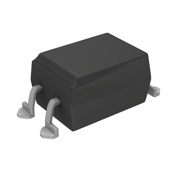
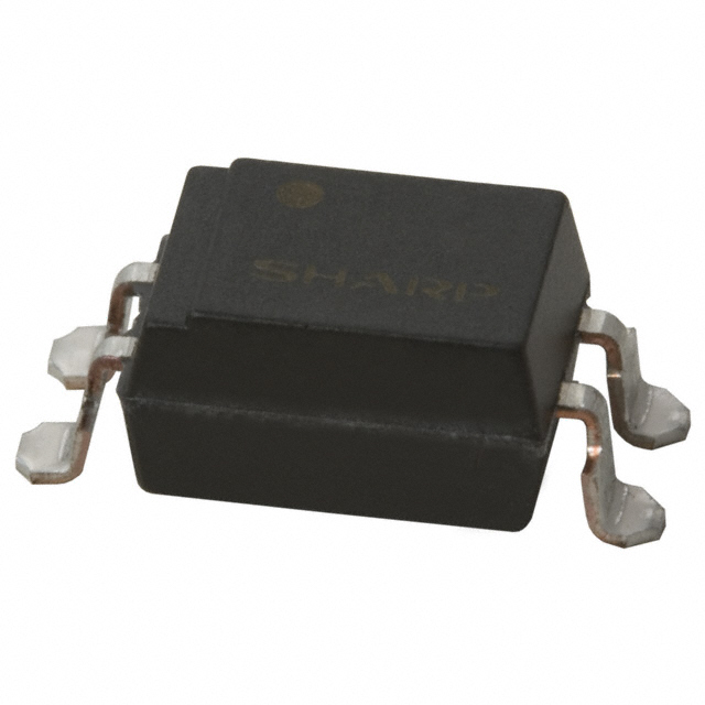
Product Overview: Sharp PC357N Optoisolator Transistor Output
The Sharp PC357N embodies the integration of a high-efficiency infrared LED with a phototransistor, utilizing an optoisolation principle to achieve electrical insulation between input and output. This configuration eliminates direct electrical connectivity, enabling safe and reliable interfacing between circuits operating at substantially different voltage levels. Internally, the input side LED converts the incoming electrical signal into optical pulses, which traverse the isolation barrier and are sensed by the phototransistor on the receiving side. The result is a faithful recreation of the input signal, free from shared ground loops or conducted noise.
Critical to industrial automation and digital logic interfacing, the PC357N features a fast response time typically less than 4 microseconds, supporting data rates suitable for most low-to-medium speed switching circuits. Its current transfer ratio (CTR) remains stable over a broad range of drive currents and ambient temperatures, a key parameter for predictable system behavior. Galvanic isolation is standardized at 3.75 kV RMS, comfortable for robust protection against voltage surges—a recurring challenge in relay-driving, PLC (programmable logic controller) inputs, and power supply feedback paths. Adopting the PC357N mitigates the risks of transient malfunction or component degradation resulting from high-voltage spikes, which routinely occur in motor control boards and power management modules.
From an integration perspective, the compact 4-pin DIP package supports high-density PCB layouts and automated assembly, reducing the likelihood of board-level faults during manufacturing. The low forward voltage requirement on the input LED eases power supply design, minimizing waste heat and supporting energy-efficient architectures. This aspect becomes nontrivial in large-scale deployments or applications with stringent power budgets. In practice, the PC357N streamlines EMC compliance, as optical decoupling greatly suppresses common-mode noise propagation across sensitive subsystems.
Practical deployment in environments with variable EMI shows the PC357N resists spurious switching—an outcome not only of the physical isolation but also the intrinsic noise immunity of the optotransistor configuration. The component’s performance under repeated high-voltage cycling reinforces confidence in system longevity, particularly in repetitive switching tasks common to switching power supplies and isolated UART circuits. Its high CTR margin allows for flexible interfacing to 3.3V or 5V logic without additional amplification or signal conditioning, thus shortening design cycles and reducing BOM complexity.
A significant insight emerges when balancing cost and reliability: the PC357N provides a blend of proven technology and supply assurance, supported by Sharp’s mature production ecosystem. Sourcing risk is minimal, and multiple second-source options from compatible vendors exist, guarding against allocation disruptions. Design teams benefit from a simplified qualification process, as the PC357N meets a broad range of international safety and regulatory standards by default, accelerating overall project timelines.
Selecting the PC357N as an isolation element moves design focus upstream—towards functional optimization rather than basic safety mediation. The net effect is a streamlined system architecture that reliably addresses isolation requirements in both legacy and advanced embedded platforms.
Key Electrical and Isolation Characteristics of PC357N
The PC357N exemplifies a class of optoisolators engineered for robust electrical isolation in mixed-voltage applications. Its rated isolation voltage of 3750 Vrms derives from precise materials choice, internal creepage distances, and encapsulation techniques, establishing a reinforced safety barrier between input and output domains. This magnitude of isolation enables fault-tolerant system partitioning, particularly within industrial automation, medical instrumentation, and high-voltage power control platforms, where separation minimizes the risk of ground loops, transient surges, and common-mode noise propagation.
At the heart of the PC357N is a gallium arsenide infrared-emitting diode optically coupled to a silicon NPN phototransistor. When a control signal energizes the input, photon emission triggers the output transistor without galvanic continuity. This optical coupling mechanism not only ensures low propagation delay and adequate bandwidth for logic-level switching but also eliminates vulnerability to high-potential shorts or invasive leakage currents. The transistor output’s open-collector configuration is designed for direct interfacing with TTL and CMOS logic families, providing flexibility in pull-up arrangements and supporting wired-OR connections. Such compatibility simplifies signal translation tasks and supports monitoring, state detection, and relay driving tasks in digitally managed designs.
In practice, ensuring optimal performance with the PC357N necessitates careful attention to board layout and trace separation. Maintaining adequate clearance from high-voltage traces and adhering to recommended pad geometry preserves the device’s isolation integrity under fault and transient conditions. Additionally, configuring the LED input drive within specified forward current ranges avoids saturation artifacts and unwanted response delays, sustaining predictable switching characteristics across operating temperature ranges.
This isolation strategy not only aids in the pursuit of compliance with IEC and UL insulation standards but addresses latent safety concerns in pre-certification prototypes. The field-proven reliability of the PC357N also minimizes nuisance triggering and crosstalk, features especially valued in process control and signal monitoring assets challenged by noisy or unstable supply domains.
The integration of robust optoisolator characteristics with universal output topology situates the PC357N as an indispensable component in the modern engineer’s isolation toolkit. By delivering both electrical separation and versatile logic handling, the device closes critical gaps in system-level design, favorably influencing long-term reliability and easing regulatory validation workflows. This convergence of safety, circuit flexibility, and regulatory alignment defines its ongoing relevance in advanced electronic assemblies.
Physical Package and Channel Configuration of PC357N
The Sharp PC357N adopts a 4-mini-flat (4-pin MFP) package, leveraging its minimized outline for densely populated PCBs and stringent spatial constraints. The streamlined form factor—typically dimensions near 4.4 mm × 2.6 mm × 3.4 mm—not only reduces board real estate consumption but also enhances pick-and-place compatibility for automated assembly lines. This geometric optimization facilitates higher throughput in mass production, decreases the potential for mechanical misalignment, and lowers the risk of soldering defects by providing consistent pin orientation and lead coplanarity.
Electrically, the single-channel internal arrangement yields a straightforward optical coupling path. The input LED and output transistor are separated by a precise insulating barrier, effecting creepage and clearance distances that meet safety requirements in isolated signal channels. The simplistic, unidirectional configuration supports unambiguous channel tracing, which proves advantageous during schematic capture and PCB trace routing—especially in power and signal integrity-critical domains. It naturally supports the elimination of crosstalk risk, privileging deterministic design analysis in functional safety or EMI-sensitive environments.
Application flexibility traces directly to the package's modular nature. In control circuitry upfitting or iterative prototype expansion, this unit scalability enables direct duplication of interface blocks without bespoke PCB modifications. For example, in PLC digital input arrays or microcontroller IO extension modules, the physical form and channel partitioning of the PC357N streamline layout duplication, resource allocation, and thermal management on multi-channel assemblies.
Assembly reliability in field deployments further benefits from the symmetrical lead positioning and rigid body mold. The package mitigates stress propagation to solder joints under temperature cycling or vibration, a common reliability challenge in industrial automation or vehicular electronics. Integrated into boards with high-speed pick-and-place operations, yields are most optimal when the standardized outline is utilized, with negligible loss to adjacent component placement density.
A key insight emerges in recognizing how the single-channel package orientation empowers modularized design architectures. By distributing individual coupling elements, rather than aggregating multiple channels into a single package, circuit reconfiguration and diagnostic isolation improve markedly. Design rebuttals to single-point failures or accidental overloads may thus be managed via granular component-level replacement and targeted fault isolation, enhancing maintainability and extending operational uptime in modular field systems. This structural approach harmonizes well with modern engineering imperatives for both production agility and long-term serviceability.
Environmental Classification and Certification of PC357N
Environmental classification and certification of the PC357N form the foundation for its integration into sensitive and high-stakes environments. The component meets globally recognized environmental criteria, addressing concerns over temperature extremes, humidity fluctuations, and continual exposure to mechanical stress. By complying with international standards—such as RoHS directives, REACH regulations, and specialized automotive-grade certifications—the PC357N presents a robust solution for projects governed by regulatory rigor. The rigorous qualification protocols include accelerated life testing, thermal cycling, and vibration analysis, reflecting conditions routinely faced in factory automation, advanced HVAC systems, and vehicle control units.
This environmental resilience not only maintains signal integrity and operational stability in electrically noisy or mechanically dynamic settings but also mitigates premature failure risks. The traceability enabled by certification fosters transparent audit trails, which accelerate both root-cause analysis and warranty processing in the event of a field issue. Such traceability—typically embedded via batch coding and digital documentation—serves as a critical asset for supply chain managers who navigate compliance audits across jurisdictions.
In practice, deploying the PC357N in control boards for railway electronics demonstrates its reliability under persistent thermal stresses and repetitive shocks. The consistency in performance across distinct installation scenarios, from high-altitude communication relays to sealed engine compartments, underscores design robustness. Unexpected power cycling and exposure to industrial solvents are similarly addressed through material selections validated as part of the environmental certification workflow.
A layered approach to qualification unlocks significant design and operational efficiencies. By integrating components pre-certified to stringent environmental benchmarks, engineering teams can expedite product development cycles, sidestep protracted in-house qualification, and focus R&D efforts on system innovation. This proactive strategy not only reduces lifecycle costs but also enhances market agility, allowing for rapid adaptation to emerging compliance requirements.
A critical insight emerges: certification should be viewed not merely as a means of regulatory conformity, but as an enabler of system-wide reliability, maintainability, and traceability. Components such as the PC357N, certified and tested beyond baseline standards, form the backbone of resilient electronic architectures—especially where operational failure translates directly into downtime or safety risk. This perspective shifts procurement and design criteria toward a more holistic appreciation of environmental robustness as a competitive advantage.
Potential Equivalent/Replacement Models for Sharp PC357N
The task of identifying equivalent or replacement parts for the Sharp PC357N optoisolator requires systematic scrutiny of core device attributes. At the fundamental level, optoisolators function to provide galvanic isolation between input and output circuits, leveraging internal phototransistor technology to mitigate signal integrity risks and minimize ground loop issues. The key performance metrics—such as isolation voltage and CTR (current transfer ratio)—directly affect system safety and response dynamics, particularly in environments subject to transient voltages or electrical noise.
When evaluating potential replacement models like the Toshiba TLP357 or the NEC PS2561L, engineers must prioritize data sheet congruence, not only at headline specifications but within the nuanced operational details. For example, differences in trigger LED current or output collector-emitter saturation voltage, even if minor, can manifest as undesirable timing skew or loading effects in high-density input stages. The structural packaging, whether DIP or surface-mount variants, must align with the host PCB’s clearance and creepage constraints to preserve regulatory compliance.
Certification markings—including UL, VDE, or CSA—often serve as gatekeepers in applications demanding documented isolation integrity for global market access. Thus, alternate devices of interest must provide parallel standards footprints and manufacturing traceability, ensuring seamless integration into production flows or field replacements. Pin configuration equivalence is particularly critical in retrofit or maintenance scenarios; mismatches lead to extensive board rework if not addressed early in the design validation process.
Pragmatic deployment reveals that component tolerance corridors sometimes lead to subsystem derating or selective reinforcement, especially under thermal cycling or power line disturbance conditions. It is advisable to benchmark replacement CTR values at multiple test points across voltage and temperature extremes, confirming robustness beyond nominal ratings. For cost-sensitive applications, lead time and supplier availability further enter into the evaluation matrix; fostering relationships with multiple vendors or utilizing authorized distribution channels can alleviate the risk of unforeseen shortages.
The real leverage in component substitution emerges when the replacement not only matches the Sharp PC357N’s performance envelope but also introduces incremental benefits. Some modern equivalents offer improved input threshold uniformity, extended operating temperature, or enhanced EMC immunity, yielding broader application latitude. As supply chain fluctuations continue to challenge procurement cycles, adopting a flexible design mentality—building in pin-to-pin and electrical interchangeability where possible—enables rapid qualification of substitute devices without undermining end-system reliability.
A disciplined approach, blending granular technical analysis with strategic sourcing intelligence, ensures that every equivalent selection is validated against comprehensive system requirements. This layered methodology not only sustains performance continuity but unearths potential optimizations in legacy designs, reducing lifecycle risks and sustaining competitive advantage.
Conclusion
Application-specific evaluation of the Sharp PC357N necessitates a granular understanding of its core mechanisms and practical trade-offs. At its foundation, the high isolation voltage—typically rated at 3.75 kV RMS—extends the operational envelope for linkages between low-voltage control circuitry and high-potential power domains. This is particularly meaningful in industrial automation, renewable energy inverters, and medical devices, where galvanic isolation mitigates disruptive ground loops and constrains transient propagation. Integrating the PC357N into such architectures requires precise assessment of insulation clearance, creepage distances, and system safety certifications, considering evolving regulatory frameworks and standards like UL or VDE.
The device’s optically coupled phototransistor output brings both versatility and predictable response characteristics. It delivers reliable on-off signaling with minimal leakage current, supporting digital logic-level interfacing as well as simple analog feedback loops. However, its CTR (current transfer ratio) variation across temperature and aging must be accounted for, especially where consistent threshold detection is critical. Deploying the PC357N in signal isolation roles for programmable logic controllers or relay drivers benefits from pre-characterized input-output mapping and proactive margining, which guards against drift and system-level parametric shifts.
Packaging details further intersect with installation constraints and long-term manufacturability. The compact 4-pin DIP or SMD variants enable high-density PCB layouts, advantageous in modular embedded systems where board real estate is at a premium. Automated pick-and-place assembly is fully supported by the standard form factor, reducing dependency on bespoke process adjustments. Procurement reliability is bolstered by the part’s broad market presence and established qualification cycles, collapsing sourcing risk and ensuring lifecycle continuity for volume production.
From a supply chain engineering perspective, the PC357N stands out by bridging rigorous application demands with mature logistical support. Certified conformity, mass availability, and proven field performance collectively streamline inventory management and technical approval cycles. Direct experience shows that early cross-functional alignment—synced among design, sourcing, and compliance teams—yields smoother project milestones and fewer late-stage redesigns. Notably, the integration window for the PC357N often outpaces alternatives, as its specification stack maps cleanly to diverse isolation use cases without mandating custom firmware or extensive validation.
Ultimately, the strategic selection of the PC357N is shaped by its layered fit to both electrical interface requirements and real-world operational constraints. Its deployment is less about choosing a commodity coupler than about embedding a reliable node in the signal chain—one that supports scalable architectures, predictable safety margins, and frictionless procurement. Approaching its selection as a function of system-level fit and supply continuity, rather than standalone component performance, delivers clear engineering and operational advantages.