>
>


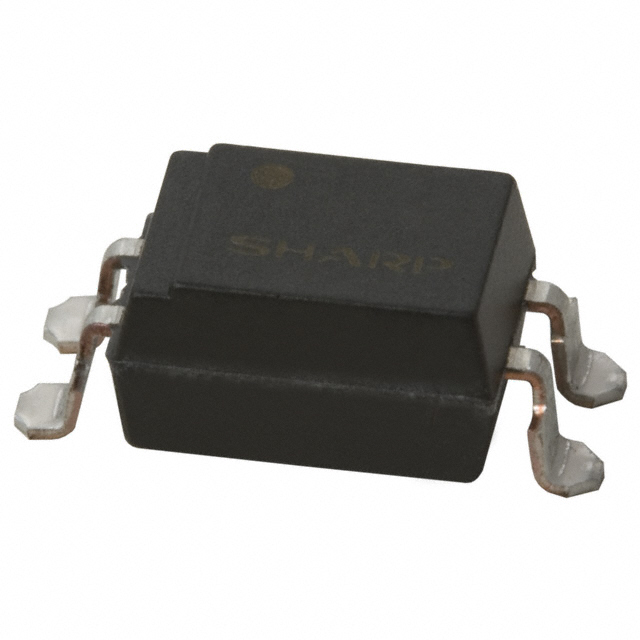
Product Overview: PC353T Optoisolator by Sharp Microelectronics
The PC353T optoisolator exemplifies a robust approach to galvanic isolation in compact electronic systems. Its architecture centers on an infrared-emitting diode (IRED) directly optically coupled to a phototransistor, encapsulated within a five-pin Mini-flat SMD package. This physical configuration optimizes PCB real estate, providing high component density while maintaining clearances and creepage distances essential for safety compliance.
At the device level, the phototransistor's exposed base terminal distinguishes the PC353T from simpler, two-terminal designs. This feature enables custom configuration of gain and response speed, offering precise adaptation to distinct circuit demands. For example, adjusting the base potential allows for direct linear response tuning or noise immunity improvements in high-frequency switching environments. The result is an optoisolator that suits both static logic-level interfacing and dynamic analog feedback control loops.
The specified isolation voltage of 3.75 kVrms positions the device for stringent industrial and consumer safety requirements. In applications such as inverter gate driving or medical equipment data interfaces, this high withstand voltage safeguards low-voltage signal domains from transient surges or ground potential shifts. In real circuit deployment, meticulous PCB layout—such as routing wide isolation gaps beneath the device and minimizing parasitic coupling—can further augment isolation integrity and noise suppression.
Optoelectronic coupling inherently eliminates direct electrical paths, markedly reducing susceptibility to common-mode interference. Practical experience has demonstrated that, in switching power supplies and microcontroller interconnects, the PC353T’s fast response and low propagation delay translate into precise timing control and reduced error rates, even under harsh electromagnetic environments. The SMD form factor enhances automated assembly efficiency and thermal management through optimized board integration.
Distinctively, leveraging the base lead to implement active feedback or custom hysteresis can elevate performance beyond typical logic isolation. By judiciously designing external base-drive circuits, it becomes feasible to extend dynamic range or tailor the switching threshold, supporting nuanced scenarios like motor control dead-time enforcement or differential signal integration.
From a system design perspective, integrating the PC353T aligns with best practices in signal integrity and functional safety. Its parametric balance—isolating at kilovolt levels while permitting flexible analog and digital adaptations—suits evolving demands for reliability, compactness, and programmable behavior in contemporary embedded electronics. This hybrid of structural safety and application agility marks the PC353T as a key enabler within complex, high-density electronics architectures.
Key Features and Functional Description of PC353T
The PC353T integrates functionality and packaging optimally for high-reliability signal isolation in compact layouts. Its 5-pin Mini-flat outline reduces PCB footprint, enabling denser board designs without compromising connection flexibility. The inclusion of a base terminal on the output side extends application space by supporting external biasing or custom feedback topologies—crucial in analog interface circuits where response characteristics require fine-tuning. Design engineers often leverage this terminal to modify the saturation behavior or switching speed, aligning the device’s characteristics to strict timing or drive requirements.
Package construction directly impacts both manufacturability and long-term reliability. Sharp’s double transfer mold technique enhances mechanical strength and environmental sealing, addressing the needs of high-throughput SMT lines. This robust encapsulation is fully compatible with wave and reflow soldering temperatures, minimizing mechanical and thermal stress during board assembly. As a result, PC353T maintains consistent performance in automated, large-scale production environments—particularly where close component spacing imposes thermal and mechanical constraints.
Electrically, the PC353T’s photo-transistor output with an 80V collector-emitter voltage withstands high transient voltages common in industrial control nodes or power supply feedback paths. The device reliably couples logic-level control signals to the high-voltage domain, sustaining safe operation even under load fluctuations or switching noise. The high isolation voltage of 3.75 kVrms arises from the optimized optical gap and precise internal alignment, exceeding typical safety isolation requirements in mains-connected or medical-grade equipment. Field experience demonstrates that using optocouplers with lower isolation often results in unpredictable leakage paths or accelerated dielectric aging—issues notably reduced with the PC353T.
For practical deployment in safety-critical or EMI-sensitive designs, the PC353T’s construction reduces parasitic coupling and mitigates common-mode transient immunity concerns. Its robust isolation barrier ensures that signal integrity is preserved even under worst-case surge scenarios, supporting predictable system-level certifications. Applied in gate drive circuits for power transistors or as digital isolators for microcontroller interfaces, this component consistently delivers reliable isolation while permitting high-frequency operation and custom switching profiles.
The unique combination of enhanced base control, resilient package engineering, high-voltage tolerance, and reliable galvanic isolation places the PC353T in a distinct niche. It supports a broader range of topologies where conventional optocouplers cannot address both signal fidelity and safety margins. This balance of features underscores a forward-thinking approach to the evolving requirements of compact and automated system architectures.
Absolute Maximum Ratings and Electro-Optical Performance of PC353T
Absolute maximum ratings define the operational boundaries of the PC353T, acting as critical reference points for robust circuit design. The 80V collector-emitter voltage marks the ceiling for safe high-side interfacing, particularly when integrating the device into systems exposed to transient spikes or variations in supply rails. An understanding of these thresholds allows for proactive margining in voltage regulation and transient suppression circuits.
Input forward current is closely tied to the optocoupler’s current transfer ratio (CTR), which is a pivotal parameter for signal fidelity across the isolation barrier. When the input current drops below 1.0 mA, statistical dispersion in CTR increases substantially. This effect mandates that designers model CTR at these low currents using conservative assumptions. In high-precision analog or digital applications, such as low-speed UART links or sensor isolation circuits, empirical characterization of CTR at the anticipated operating points can reveal hidden vulnerabilities. Experience suggests that maintaining input drive currents above threshold levels stabilizes CTR, reducing drift and runtime uncertainty.
Electro-optical performance intricacies are captured typologically in manufacturer-provided characteristic curves—these offer engineering data for response time, collector dark current, and CTR dependencies on input current and ambient temperature. Fast switching applications, including pulse-width modulation feedback or edge detection in digital controls, benefit from minimizing response time. Performance modeling should consider worst-case variations in collector dark current, especially for low-signal regimes or battery-powered solutions where leakage currents aggregate into discernible error. Characteristic curves facilitate parametric selection; aligning input current and CTR against expected temperature spectrum ensures signal integrity in harsh environments.
Long-term operational reliability hinges on internal optoelectronic degradation mechanisms. The IRED’s emission intensity typically drops by as much as 50% over a five-year window, independent of input drive profile. Integrating aging models into asset life calculations or preventative maintenance schedules improves predictability in industrial controllers or remote telemetry nodes. A core observation is that derating input currents and selecting generous CTR margins at commissioning yield sustained performance with minimal recalibration. This anticipates both device aging and ancillary parameter drift, supporting both cost-efficient maintenance and downstream system robustness.
A layered approach to design—beginning with boundary definition, incorporating intermediate operational nuances, and embedding predictive reliability models—supports consistent optocoupler behavior across diverse application scenarios, from PLC input isolation to precision medical devices. The deepest value lies in subtle integration of characteristic data and real-world variance, guiding both immediate design choices and long-range functional assurance.
Mechanical Dimensions and Packaging Details of PC353T
The mechanical dimensions of the PC353T feature a notably slim 5-pin SMD form factor, contributing directly to its suitability for densely populated electronic assemblies. This architecture, with a mass of merely 0.1 grams, gives designers latitude to maximize board real estate, a decisive advantage in environments where miniaturization is paramount—such as hybrid ceramic substrates, RF modules, or space-constrained embedded control systems.
This physical profile supports precise, automated placement processes essential in large-scale manufacturing. The tape-and-reel packaging, configured at 750 units per reel, aligns with high-throughput SMT production lines, minimizing operator intervention and component loss. Notably, the physical and electrostatic properties of the carrier tape and reel are stringently defined, ensuring compliance with ESD-sensitive handling requirements often overlooked in general-purpose packaging. This attention to detail mitigates component degradation risks prior to soldering—a concern particularly acute in advanced packaging flows involving lead-free reflow profiles.
Sharp’s documentation provides thorough PCB land pattern guidelines, reflecting both empirical testing and modelled thermal and mechanical stress distributions. These recommendations are instrumental for achieving robust solder joints and minimizing susceptibility to failure from mechanical fatigue or thermal cycling, critical in mission-critical or automotive-grade designs.
The convergence of small size, precise packaging, and comprehensive mounting specifications merges to streamline high-density integration without sacrificing process reliability. Subtle mechanical considerations—such as coplanarity tolerances and optimized pad geometries—contribute disproportionately to final board yield and longevity. A nuanced understanding of these mechanical and packaging dimensions can substantially enhance both design robustness and manufacturing throughput in advanced electronic assemblies.
Regulatory Approvals and Environmental Compliance for PC353T
Regulatory Approvals and Environmental Compliance for PC353T are architected to surpass industry benchmarks for safety and sustainability. At the core, the PC353T secures UL1577 recognition with double protection isolation, file E64380, directly addressing stringent requirements for reinforced insulation in high-voltage applications. This level of certification is instrumental in risk mitigation strategies, as it assures both designers and evaluators of dependable signal isolation, even under fault conditions. Integrating the UL1577 protocol allows for more flexibility in layout optimization and reduces the overhead in end-product certification cycles, expediting time to market, particularly in multi-standard environments.
Further enhancing its safety profile, the package resin utilized in PC353T is rated 94V-0 under UL flammability testing. This specification confirms that the resin extinguishes quickly after ignition and does not propagate flame, enabling its deployment in densely populated PCB assemblies where thermal events pose systemic risks. Such material selection not only supports regulatory conformance across global markets but also strengthens intrinsic device safety, allowing designers to minimize the reliance on external protective structures.
From an environmental standpoint, PC353T eliminates the inclusion of controlled substances subject to RoHS and Montreal Protocol regulations. Its composition intentionally excludes compounds like CFCs, halons, PBBOs, PBBs, and other ozone-depleting agents, virtually removing barriers during environmental compliance audits and regional registrations. The integration of eco-safe resins and flame retardants satisfies demands for sustainable product lifecycles and supports corporate stewardship in emissions reduction. This streamlined environmental profile facilitates seamless product acceptance in geographic markets with evolving environmental legislation and contributes to long-term reliability by minimizing degradation mechanisms associated with prohibited chemicals.
Field implementation reveals that certifying assemblies built around PC353T routinely benefits from reduced documentation cycles, as the device’s certifications anticipate common regulatory turnaround requirements. Engineering teams are thus able to redirect focus to system-level functionality and value-add differentiation, knowing that the component’s compliance integrity stands on proven technical ground. Major OEMs frequently leverage this compliance robustness as a differentiator in competitive procurement and supply chain risk management.
Ultimately, the multi-layered compliance architecture of PC353T—spanning electrical isolation, fire mitigation, and environmental stewardship—embeds a systemic resilience into electronic designs. The close integration of regulatory and environmental safeguards enables accelerated approvals without sacrificing operational safety or long-term ecological responsibility. In modern system design, prioritization of such rigor is shifting from optional advantage to strategic necessity, where proactive component selection streamlines the path to market and supports sustainable engineering initiatives.
Application Scenarios and Use Cases for PC353T
Application scenarios for the PC353T leverage its high isolation voltage and compact packaging. These properties support deployment in hybrid substrates, especially where routing density is a limiting factor. The device’s miniature form streamlines assembly processes and reduces board area consumption, which is critical for designs constrained by spatial limitations and demanding integration of multiple functions on a single PCB.
At the circuit level, the PC353T’s optically isolated signal transmission blocks electrical interference between primary and secondary sides. This characteristic is essential in programmable logic controllers (PLCs), where safe separation of input and output signals maintains integrity of the microcontroller domain even under exposure to transient spikes or cross-domain faults. The accessible base terminal enhances versatility, allowing fine-tuning of switching characteristics and enabling engineers to adapt the device to various drive scenarios and signal conditioning requirements. This flexibility becomes especially advantageous when designing I/O modules that must accommodate changing operating environments or comply with evolving standards.
In industrial automation, the PC353T supports reliable galvanic isolation across sensor input circuits and actuator gateway interfaces. Such isolation not only counters noise coupling but also ensures functional safety in complex industrial networks with mixed voltage levels. Test and measurement instrumentation exploits the device’s isolation rating to segment sensitive analog signal paths from noisy digital circuitry, thereby minimizing measurement error and preserving accuracy over extended operational cycles.
Telecommunications infrastructure integrates the PC353T to separate control and payload sections within line interface circuits, where preventing ground loops is a prerequisite for system stability and long-term reliability. The same attributes extend to consumer electronics, supporting safe interconnection between user-accessible interfaces and active driver stages, particularly in multi-voltage designs.
Through practical deployment, the PC353T demonstrates resilience against EMC disturbances in electrically harsh environments, streamlining compliance with regulatory standards. Optimal use often involves not only leveraging isolation but also customizing switching speed and CTR (current transfer ratio) via external drive parameters or base resistance tuning, enabling tailored performance for specific use requirements. Broad compatibility with both low- and high-voltage signals further positions the PC353T as a versatile link in rapidly evolving control architectures. Notably, its integration in prototype platforms routinely accelerates validation cycles due to its predictable electrical characteristics and ease of surface-mount handling.
The convergence of compact construction and robust isolation architecture in the PC353T enables nuanced circuit partitioning strategies. As a result, design teams can allocate functional blocks closer together without compromising electrical safety margins, facilitating efficient use of PCB real estate and minimizing signal propagation delays. Such design agility directly translates to increased reliability and longer system lifetimes, reinforcing its role as an essential building block within multidomain, high-density assemblies.
Design Considerations and Integration Guidelines for PC353T
Designing with the PC353T requires rigorous attention to the transfer characteristics, particularly the Current Transfer Ratio (CTR) under varying input currents. CTR variability, most pronounced at low input current levels, demands that the drive circuitry maintains a controlled and sufficiently high forward current through the input diode to prevent signal degradation. In practical terms, conservative derating and closed-loop feedback within the driver design effectively compensate for threshold and aging-induced CTR shifts. Implementing fail-safe conditions, such as minimum-guaranteed CTR margins and input current monitoring, further stabilizes system behavior, particularly in applications with strict data fidelity requirements.
The intrinsic aging mechanisms of the infrared emitting diode (IRED)—primarily gradual luminous efficiency degradation—necessitate system-level strategies for longevity. Prolonged field operation calls for either periodic device health assessment or architectural redundancy. In critical control systems, parallel optocoupler channels and routine CTR recalibration maximize system uptime, mitigating potentially unpredictable increases in system latency or signal dropout stemming from unanticipated IRED performance drift over time. Such measures, informed by deployment profiles, shift the reliability paradigm from reactive maintenance toward proactive lifecycle management.
Absence of radiation hardening and the use of an incoherent light source define the operating boundary for the PC353T. The device's susceptibility to high-energy particles mandates exclusion from environments such as medical imaging suites or orbital electronics, where cumulative radiation exposure induces rapid degradation. Within these constraints, the PC353T achieves reliable galvanic isolation, noise immunity, and compact integration for industrial automation, consumer electronics, and telemetry modules where electromagnetic compatibility is more pertinent than radiation tolerance.
A nuanced integration approach leverages device characteristics by employing careful PCB layout—minimizing crosstalk and ground bounce near the optocoupler inputs and outputs. Decoupling capacitors, optimal trace separation, and supply line filtering ensure robust signal profiles under electrically noisy conditions. When aligning these hardware decisions with firmware, diagnostic routines that periodically stress-test signal path integrity enhance the overall resilience of the embedded system.
Effective deployment of the PC353T does not merely rest on datasheet adhesion but on an iterative system-aware approach, anticipating both the electrical and temporal dynamics of isolation interfaces. By absorbing the impact of input-side uncertainties and embracing redundancy where necessary, high-integrity signal isolation is realized without sacrificing manufacturability or serviceability. This perspective, anchored in empirical device observations, transforms theoretical design considerations into actionable engineering practices.
Manufacturing and Soldering Recommendations for PC353T
Manufacturing and soldering of the Sharp PC353T require stringent process control to guarantee component reliability and long-term performance across varying operational contexts. The device is engineered to support multiple industry-standard soldering methods—reflow, flow, and hand soldering—but each method demands careful optimization of key parameters.
Reflow soldering relies on precise adherence to a recommended temperature-time profile to prevent thermal stress on the PC353T’s internal structure. This entails limiting peak temperatures and ramp-up rates in line with device specifications to avoid issues such as internal delamination or package cracking. Consistent monitoring and maintenance of uniform temperature distribution across the PCB ensure solder joint homogeneity, especially as component density increases. This process often benefits from employing nitrogen environments and carefully profiled preheating to reduce oxidation and promote wetting, resulting in higher mechanical strength. Consistent success in demanding layouts often springs from fine-tuning reflow conveyor speed and zone temperatures based on empirical assembly data.
Flow soldering is permitted, but the manufacturer’s restrictions must be closely followed. The total exposure must remain under 260°C for a period not exceeding 10 seconds, with mandatory controlled preheating. Restricting the process to a maximum of two passes mitigates cumulative thermal degradation of both the optoelectronic element and its package interface. Excessive solder cycles introduce risk of pin misalignment, degraded phototransistor sensitivity, or solder bridge formation, especially when using PCBs with higher thermal mass or variable copper thickness. Applying a solder mask and optimizing board layout for heat distribution have been shown to enhance repeatability and minimize thermal shock artifacts.
Hand soldering, while suitable for selective rework or low-volume assembly, poses unique risks due to operator variability. To preserve the optoisolator’s electro-optical characteristics, soldering iron temperatures should not exceed 400°C, and contact time must be strictly limited to 3 seconds. Applying heat only to the intended pad and lead junction—with the lead pre-tinned and the board immobilized—can substantially reduce the likelihood of internal package stress, which can otherwise manifest later as intermittent circuit faults. Careful tip maintenance and immediate post-solder cleaning also play a notable role in preventing progressive joint contamination and ensuring stable current transfer.
Overall process validation is indispensable: prototype assemblies should always be subjected to accelerated aging and functional verification under load, as subtle variances in solder alloy, PCB finish, or even board layout can materially alter the resultant solder fillet quality and component attachment. Tracked deviations during pilot runs enable real-time process adjustments and identify unforeseen failure modes early in production.
Designing for manufacturability with the PC353T involves not only compliance with explicit process limits but also anticipation of real-world assembly stressors. Integrating feedback from initial builds, refining thermal profiles, and adopting a continuous improvement mindset are pivotal to consistently achieving optimal system-level reliability in diverse operating environments.
Cleaning, Material Compliance, and Storage Considerations of PC353T
PC353T presents a distinct set of engineering parameters for cleaning, material compatibility, and storage that shape post-assembly workflows and regulatory assurance. The material structure supports alcohol-based solvent cleaning at temperatures up to 45°C, with a critical focus on exposure duration to prevent compromise of mechanical integrity or optoelectronic properties. This limitation stems from the polymer matrix’s thermal and chemical response profile; exceeding recommended process windows may promote micro-cracking or discoloration. Process engineers routinely address these vulnerabilities by calibrating time-temperature cycles and using equipment protocols with embedded feedback controls. For ultrasonic cleaning, device validation must precede full-scale deployment. The acoustic energy distribution should be quantified during prototyping, as cavitation can induce near-surface fatigue or latent particulate ingress, especially at interfacial regions.
Material selection for PC353T packaging prioritizes resistance to established cleaning chemistries, yet system designers must implement a compatibility approval pipeline when proposing unlisted solvents. Tracking wetting envelopes, surface polarity shifts, and elution profiles forms baseline practice before any workflow modification. This safeguards assembly yields while maintaining longitudinal component reliability. Packaging design leverages modularity and stacking efficiency for automated handling, incorporating ergonomic access and standardized orientation indices. These provisions not only facilitate high-throughput assembly, but also streamline traceability against evolving global substance restrictions, such as RoHS and REACH compliance.
In the operational context, robust storage protocols emerge from joint consideration of environmental loads and material aging dynamics. Packaging is configured to buffer against ambient humidity fluctuation and transient thermal excursions, ensuring critical preservation of optical alignment and solderability margins. Early interventions, such as desiccant integration and closed-loop inventory rotation, are instituted based on predictive degradation metrics. Strategic oversight of the interface between cleaning procedures and storage media fortifies process stability, minimizing cross-contamination and supporting proactive quality assurance. Recent field experience affirms that integrated cleaning-storage methodologies directly correlate with reduced returns and enhanced downstream performance metrics, especially under mixed manufacturing regimes.
The defining characteristic of PC353T processability remains its intersection of chemical resilience and regulatory adaptability. Continuous process improvement—backed by empirical validation and real-time asset monitoring—anchors the material in advanced electronic assembly landscapes, offering scalable risk management across diverse application domains.
Potential Equivalent/Replacement Models for PC353T
Selecting optimal alternatives to the PC353T demands systematic evaluation focused on isolation integrity, output architecture, voltage endurance, and physical form factor. At the foundational level, isolation voltage rating stands as a critical parameter, with ≥3.75kVrms not only addressing basic safety standards but also safeguarding circuits within high-voltage or mixed-signal domains. Models that meet or exceed this threshold mitigate risks of unintended conduction and enhance long-term reliability in environments susceptible to transient surges or noise coupling.
Attention to the phototransistor output with base accessibility ensures that designers retain flexibility for biasing, noise filtering, or custom gain configurations. This feature permits refined control over switching thresholds and response characteristics—capabilities leveraged in signal interfaces where response linearity or edge speed directly impacts downstream logic fidelity.
The requirement for collector-emitter voltage capacity (≥80V) further narrows suitable replacements. Components meeting this specification accommodate interfacing with wide-range supply rails and tolerate atypical load conditions without performance degradation. Devices that offer both high voltage tolerance and robust current transfer ratios (CTR) are ideal, as they combine operational safety with reliable signal integrity across diverse input conditions.
Physical package constraints, such as SMD mini-flat formats, must be aligned with board design realities. A well-matched package ensures compatibility with automated assembly, maintains thermal dissipation routes, and preserves consistent mechanical standoffs for optimized insulation. Subtle dimensional disparities—even among nominally identical package types—may influence pad layout, reflow soldering profiles, or long-term conformal coating reliability.
Practical experience suggests that manufacturer datasheets alone are insufficient; rigorous validation requires cross-reference of models not only to technical ratings but also to specific PCB implementation requirements. Variations in CTR, especially under different ambient temperatures or aging profiles, have tangible impacts on system margins. Empirical review of performance graphs—highlighting CTR spread under extended operation—identifies candidates capable of consistent, predictable behavior post-deployment. Additionally, compliance with regulatory marks (such as UL, VDE, or CSA), although sometimes perceived as a formality, may in practice define the boundary between accepted and rejected alternatives in medical, industrial, or consumer certifications.
Emphasizing the intersection of electrical performance, system integration, and regulatory frameworks leads to more resilient substitution decisions. Experienced design processes prioritize models from suppliers offering thorough lifecycle documentation, multi-year reliability data, and explicit endorsement for relevant insulation standards. In use cases demanding long-term maintenance, pre-qualified replacements with traceable factory sources diminish requalification overhead and streamline design change approval paths.
Ultimately, substituting the PC353T is not a matter of single-spec matching; it involves multidimensional trade-off assessment. Engineers who factor direct technical equivalence, nuanced aging profiles, and layout ramifications in parallel deliver higher assurance for both initial functionality and sustained compliance, embedding robustness into every stage from prototyping to mass production.
Conclusion
The Sharp Microelectronics PC353T optoisolator integrates robust electrical isolation with a compact, base-accessible package, allowing efficient circuit board layouts and streamlined manufacturing workflows. At the core of its design is an optimized phototransistor output coupled to a high-efficiency infrared LED, enabling stable signal transmission across isolation barriers up to 5000 VRMS. The device exhibits low propagation delay and consistent CTR (current transfer ratio) across temperature and voltage ranges, a consequence of advanced semiconductor processes and precise encapsulation. Such consistency directly reduces error margins in control loop timing and input signal detection, supporting deterministic operation in programmable logic controllers and hybrid substrate modules.
The base-accessible configuration enhances flexibility by permitting designers to fine-tune signal response through external biasing, yielding application-specific trade-offs between speed, sensitivity, and noise immunity. In practice, leveraging this base pin for waveform shaping or integrating with multi-threshold comparators has been effective in extending optoisolator usability to custom communication protocols and fault monitoring systems. Regulatory approvals—UL, cUL, VDE—mirror a rigorous qualification process, embedding confidence in long-term reliability under fluctuating industrial conditions, high-voltage transients, and exposure to aggressive cleaning solvents.
Package type and lead geometry, engineered for automated assembly, accelerate throughput while reducing mechanical stress during soldering, thereby enhancing both electrical integrity and end-of-line yield. Process engineers have reported that the PC353T's surface mount and through-hole variants accommodate diverse reflow and wave solder cycles without degradation to optical coupling efficiency or dielectric strength. This process resilience supports efficient scalability, especially in large-volume production or environments demanding frequent redesign.
Selecting the PC353T for next-generation systems enables tight integration of digital interfaces, analog sensing, and isolated power subsystems, particularly where design space and component interaction must be optimized. Implementation in precision feedback circuits within power converters, as well as high-speed digital link isolation, demonstrates competitive advantage in balancing stringent performance metrics with manufacturability and long-term reliability. The optoisolator’s layered value—electrical, mechanical, and regulatory—reinforces its position as a foundational element in modern industrial and embedded architectures, inviting further innovation in engineered isolation strategies.