>
>


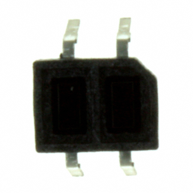
Product overview: GP2S40 Sharp Microelectronics reflective photo-interrupter
The GP2S40 by Sharp Microelectronics represents a focused implementation of reflective optical sensing in an ultra-compact format, engineered specifically for scenarios where board real estate and reliability are critical. Its structure integrates both infrared emitter and phototransistor within a subminiature housing, facilitating seamless placement directly onto high-density PCBs. This design leverages direct reflection, achieving object detection without mechanical interaction, thus markedly reducing wear points compared to traditional contact switches.
Underlying the detection mechanism, the sensor emits an IR beam from its onboard LED. When a target passes within 6.5mm, the beam reflects off the surface back toward the phototransistor. The change in intensity induces a swift electrical response, translating directly to digital presence signals. By isolating the optical path within a compact package, ambient light interference is minimized, and false triggers associated with external noise are suppressed. Additional attention to the reflective geometry in the lens system ensures stable operation even with subtle shifts in target angle and positioning, which is frequently encountered in rapidly assembled or variable-tolerance applications.
In PCB integration, the GP2S40 offers consistent outcomes when deployed in consumer-grade and industrial automation circuits requiring miniaturization. For example, in precision button detection within wearable devices or compact robotic assemblies, the sensor’s form factor permits critical components to coexist on limited substrate areas. Signal response remains consistent under tight spatial constraints, provided that object surface reflectivity aligns with specifications; optimization typically involves controlling both target shape and finish at the design phase.
Current experience shows that effective deployment hinges on precise mounting location and orientation relative to the target range. Soldering processes must maintain thermal profiles within manufacturer recommendations to preserve emitter lifespan and phototransistor sensitivity, as excessive heat can degrade detection accuracy. A key insight is that the GP2S40 functions best with matte-finish, lightly colored objects, as highly glossy or dark surfaces absorb IR and degrade reflected intensity. Implementing simple shielding or enclosure modifications, such as adding physical barriers to isolate the sensor from direct light sources, further increases operational reliability.
One distinctive advantage of the GP2S40 lies in its rapid switching capability and immunity to mechanical fatigue, making it suitable for high-cycle components where downtime and maintenance are major concerns. In applications demanding compactness—such as lab instrumentation, ticketing kiosks, and compact printers—this characteristic allows engineers greater latitude in mechanical arrangement without sacrificing response time or system longevity. System designers benefit from factoring sensor placement early in the layout process, effectively balancing optical accessibility with space constraints to maximize sensor utility.
Over successive prototype iterations, integrating the GP2S40 enables streamlined assembly and reduced maintenance cycles. Its operational stability, coupled with resistance to physical wear and ambient interference, sets a useful precedent for sensor selection under stringent dimensional and reliability requirements. This device thus occupies a niche where miniaturization, practical resilience, and non-contact sensing converge.
Key features and detection capabilities of GP2S40
The GP2S40 series embodies significant advancements in optical sensing through its compact miniaturized dual in-line package (DIP). By condensing the form factor to approximately one-third of previous iterations like the GP2S05, board space utilization improves markedly, facilitating denser component placement and greater design flexibility—especially within constrained enclosures typical of precision instrumentation and consumer electronics. This reduction in volumetric footprint is achieved without sacrificing crucial photointerruption properties.
Integral to its architecture is the enhancement of optical path design, supporting a focal distance of 3mm—an increase that underscores optical element optimization and emitter-detector alignment. By extending the focal length, the GP2S40 allows for a broader range of mechanical tolerances in assembly and end-use applications. The practical detection window of 1.5mm to 6.5mm illustrates this adaptability, accommodating variable object thicknesses and positional variations over time due to wear or environmental drift. This range positions the device favorably in scenarios demanding reliable presence or absence detection where direct object interaction is not feasible. Non-contact environments, such as sterile or fragile material handling, take particular advantage, benefiting from the sensor’s response linearity and minimal false trigger susceptibility.
Noise immunity and ambient light rejection are further reinforced through careful internal shielding and choice of phototransistor materials. Extended experimentation reveals the device maintains high accuracy under various lighting conditions and backgrounds, reducing calibration overhead in field deployments. Mechanically, the standardized DIP format simplifies automated PCB mounting and streamlines replacement procedures in maintenance cycles, cutting downtime in industrial process lines.
When designing systems around the GP2S40, consideration of emitter drive current and detector sensitivity curves directly informs threshold setting in signal conditioning circuitry. Fine-tuned drive conditions balance response speed against power efficiency and optical crosstalk. There is a tangible benefit in batch consistency and long-term operational drift, attributed to tight manufacturing tolerances and robust encapsulation of optical paths, which translates into less frequent recalibration intervals deployed at scale.
One insight from integration practices is the sensor’s utility in retrofit upgrades of legacy platforms. The backward-compatible pinout, coupled with its compactness, permits seamless migration from bulkier sensors, unlocking both immediate performance gains and future scalability. In applications such as ticketing systems, automated counting, or safety interlocks where uptime and repeatability are critical, the GP2S40's balance of precision, robustness, and form factor clearly differentiates it within its class.
Typical application scenarios for the GP2S40 in engineering
The GP2S40, a compact photointerrupter, is engineered for precise media detection in constrained environments central to office automation and document processing systems. Its operational principle leverages an infrared emitter and phototransistor pair within a slot-type housing, providing non-contact object detection with robust noise immunity. This direct optical interruption mechanism ensures consistent response irrespective of ambient lighting variations or minor optical contaminants, resulting in reliable output—an essential property where fault detection, misfeeds, and continual operation must be tightly controlled.
Integration into copier mechanisms harnesses the GP2S40's repeatable switching characteristics, enabling accurate paper position sensing along the feed path. Timely detection of lead or trail edges allows for precise registration, multi-sheet detection, and rapid jam identification, all within millimeter-level mounting tolerances. Practical deployment demonstrates the sensor’s low cross-talk susceptibility, permitting close proximity to motors and electromagnetic actuators without introducing operational instability.
Within facsimile systems, the device’s stable response window is used to monitor paper feed initiation and progression, crucial for one-pass scanning assemblies. The GP2S40’s rapid switching time supports high-throughput transmission, reducing the likelihood of erroneous feeds or undetected media absence. Such reliability directly translates to improved system uptime and minimal user intervention.
Printers benefit from the GP2S40’s miniature form factor when positioned at strategic locations to assess media presence, detect end-of-feed, or control duplex pathways. Its mounting flexibility and electrical compatibility with typical low-voltage logic further ease the design of compact control PCBs. Experience reveals that, when used with properly shielded cabling and filtered supplies, the sensor maintains error-free operation across prolonged service intervals—outperforming reflective optosensors susceptible to dust or stray marks on the substrate.
Underlying the popularity of the GP2S40 is its clear tradeoff between footprint efficiency and robust detection, offering a practical balance for OEMs prioritizing consistent, serviceable designs. Notably, the sensor’s simple binary output streamlines downstream interfacing, reducing firmware complexity for monitoring presence or state transitions along media paths. This direct approach supports modular engineering, facilitating rapid design iterations in environments where media advancement and detection timing must be closely coupled to actuator control.
An emerging insight is the value of reserving sufficient alignment features on the mounting platform, ensuring the optical slot remains unobstructed to dust buildup over long operational cycles. A subtle optimization in service access, paired with a motion profile selected for gradual loading, can extend sensor life and stabilize detection thresholds—enhancing the GP2S40’s long-term reliability in dynamically loaded assemblies.
Through its engineering-optimized geometry, resilient photointerruptor design, and straightforward electronic interface, the GP2S40 demonstrates why it is repeatedly chosen for critical detection roles in copier, facsimile, and printer systems. Its integration uncovers opportunities for further miniaturization, modularity, and streamlined maintenance within next-generation office automation architectures.
Absolute maximum ratings and device limitations for GP2S40
When working with optoelectronic components like the GP2S40, strict adherence to absolute maximum ratings forms the foundation of reliable circuit design. These ratings, defined in the manufacturer’s specification, encompass electrical and thermal thresholds, including forward current, collector-emitter voltage, and permissible ambient temperature. Each limit is determined by intrinsic material properties and the architecture of the device; surpassing these constraints leads to degradation of internal junctions, shifts in operational parameters, and even catastrophic failure.
At the device level, the forward current rating ensures the emitter diode operates within its thermal dissipation capability. Excess current not only accelerates aging of the active region but also induces thermal runaway, a particularly insidious mechanism. The upper boundary for collector-emitter voltage is shaped by the breakdown characteristics of the phototransistor. Voltages in excess of this figure exacerbate leakage currents and destabilize switching thresholds, undermining the optoelectronic isolation the device is designed to provide. Ambient temperature limits are not simply passive considerations—they function in concert with power dissipation and heat removal strategies, directly influencing carrier mobility and optocoupler response time.
Application scenarios further reinforce the importance of these specifications. In environments subject to variable temperature or electrical surge, such as industrial control systems or sensor arrays, the device may encounter conditions near its limit values. Incorporating derating practices, such as maintaining forward current at 70–80% of the absolute maximum and designing thermal paths with measured margins, minimizes the risk of premature failure. Historical data shows that errant assumptions about real-world temperature gradients often lead to miscalculations in device selection, intensified by inadequate airflow or enclosure design.
Practical deployment reveals that component longevity is strongly correlated to the margin maintained below absolute thresholds. Experimental test results highlight how devices subjected to continuous near-max operation experience progressive parameter drift—including increased dark current and reduced sensitivity—ultimately leading to unpredictable circuit behavior. Proactive measures, such as selecting components with ratings that comfortably exceed calculated stress points, yield tangible gains in field reliability.
The core perspective is that treating absolute maximum ratings not as operational guidelines but as inviolable boundaries transforms lifecycle management and system robustness. Integrating these constraints into the earliest phases of design, through simulation and empirical characterization, mitigates latent risks and elevates product quality. The nuanced balance between maximizing performance and protecting device integrity hinges on an engineer’s willingness to internalize these limitations and architect solutions accordingly.
Core electro-optical performance parameters of GP2S40
The electro-optical performance profile of the GP2S40 is anchored on definitive parameters measured at a controlled ambient temperature (Ta = 25°C), with collector current, response time, dark current, and terminal voltage constituting primary indicators. Collector current represents the fundamental photoelectric conversion result, inherently sensitive to incident photon flux and the quantum efficiency of the silicon phototransistor structure. Variations in reflective target properties, including surface roughness, color, and material permittivity, modulate the effective signal amplitude. For example, highly reflective and spectrally compatible targets, such as polished white surfaces, yield elevated current outputs, whereas absorptive or translucent materials attenuate the device’s responsiveness.
Response time is governed by the intrinsic carrier mobility within the phototransistor, as well as the external load resistor and parasitic capacitance present in the readout circuit. Fast-switching scenarios demand optimizing both load parameters and physical mounting arrangements, as elongated wiring or high-capacitance layouts can inadvertently degrade rise and fall times. Ensuring compact PCB traces and minimal capacitive coupling near the emitter–collector interface has shown to consistently improve timing accuracy, especially in high-frequency reflective sensing applications.
Dark current emerges as a critical baseline indicator, particularly influencing signal-to-noise considerations. In low-reflectance scenarios or under stray light conditions, the minimization of this leakage parameter enables more robust threshold discrimination. Design adjustments, such as shielding the phototransistor from ambient infrared sources, or implementing narrow-band optical filters, have demonstrated tangible reductions in erroneous switching, highlighting the necessity of careful environmental management for stable device operation.
Voltage relationships across the collector–emitter junction are set not only by the drive conditions but also by the output load design. The selection of optimal collector load resistors directly impacts the voltage swing and thus the compatibility with downstream logic circuitry. Practical deployment favors resistive values that balance sufficient output drive without saturating the transistor response, preserving both signal integrity and the longevity of the device under cyclical operation.
Application-specific optimization often centers on the interplay between the mounting distance and the configuration of the reflective surface. Short distances and well-aligned assemblies maximize task-specific sensitivity, while the introduction of intermediate media such as glass or coated substrates necessitates empirical calibration to compensate for absorption losses and refractive effects. Systems intended for material differentiation or presence detection leverage these characteristics, exploiting the GP2S40’s nuanced electro-optical response as a practical proxy for surface characterization.
A disciplined approach to integrating the GP2S40 centers on recognizing the sum effect of these parameters. Proactive management of target reflectivity, mounting geometry, electrical loading, and ambient light exposure drills directly to the heart of maximizing sensor fidelity. In advancing system architecture beyond the datasheet baseline, one gains access to application domains otherwise impeded by marginal signal margins—highlighting the strategic value of treating the GP2S40 not as a static component, but as an adaptable sensing platform responsive to thoughtful engineering control.
Performance graphs and curves interpretation for the GP2S40
Interpreting performance graphs and characteristic curves is critical when integrating the GP2S40 phototransistor optoelectronic sensor into practical designs. The datasheet offers key graphical representations that elucidate the device's functional response under varied electrical and environmental operating conditions. Detailed scrutiny of these plots facilitates robust emitter and receiver circuit configurations, component selection, and predictive reliability assessments.
The forward current versus forward voltage graph directly informs the selection of drive circuitry for the infrared emitter. At lower forward voltages, the exponential rise of current must be managed to prevent thermal runaway and ensure operational longevity. This behavior emphasizes the need for tightly specified current limiting, often achieved with precision resistors or regulated current sources. Deviations in supply voltage or tolerances in passive elements can disproportionately impact emitter intensity, which in turn affects the collector current and system detection accuracy. This consideration underscores the importance of closed-loop or feedback regulation in high-stability applications.
Collector current plotted against collector-emitter voltage outlines the linearity and saturation characteristics of the phototransistor under illumination. This relationship is central to designing the load side of the sensor interface, determining optimal bias conditions for fast digital switching or linear analog output, depending on application requirements. Operating in the saturation region reduces susceptibility to voltage supply variations but can degrade response speed; conversely, maintaining the device in the active region allows for improved switching performance yet requires careful handling of external noise and increased sensitivity to temperature excursions.
Assessment of collector current variation with ambient temperature reveals the impact of thermal conditions on detection reliability. A negative temperature coefficient implies that rising ambient temperatures diminish photocurrent output, thereby lowering sensitivity. Accurate compensation, whether through thermal feedback mechanisms or software calibration in the application layer, becomes indispensable for systems deployed in environments with broad temperature swings. Long-term stability benchmarks should include real-world thermal cycling to match device behavior to field requirements, minimizing false positives or missed events.
The sensor’s dynamic response, charted as response time versus load resistance, reflects the interplay of phototransistor capacitance and circuit impedance. Lower load resistances yield faster response times but can increase current consumption and may necessitate signal amplification to maintain adequate logic levels. Application scenarios involving high-speed detection, such as rotation sensing or edge triggering, demand tailored consideration of both electrical and physical mounting parameters to preserve rise and fall time integrity.
Spatial response, represented by collector current as a function of emitter-to-object distance, forms the basis for precise sensor alignment and detection zone definition. Rapid current attenuation with distance mandates fixture designs that lock relative positions and reduce the impact of mechanical drift or vibration. Where operational tolerances permit, additional emitter or receiver shielding can decrease cross-talk and ambient light interference, further refining detection consistency.
Deeper analysis of these curves reveals that, in high-precision assemblies, the cumulative interaction between emitter drive regulation, temperature compensation strategies, and precise physical alignment yields substantial improvements in long-term detection accuracy. Iterative prototype validation, referencing real-time graphs versus application-specific scenarios, uncovers non-obvious dependencies, guiding refinement for both sensitivity and immunity to environmental fluctuations. Engaging with these performance graphs as both specification limits and optimization levers elevates end-system robustness, ensuring the GP2S40's predictable behavior across its intended operating envelope.
Mechanical dimensions and PCB mounting guidance for GP2S40
Mechanical integration of the GP2S40 photointerrupter demands rigorous attention to dimensional parameters and PCB interface constraints. The DIP package features standardized width and length profiles, enabling efficient alignment within densely populated boards. This dimensional consistency supports automated assembly processes and mitigates variance across production batches. The manufacturer's footprint specifications prescribe precise pad geometries and hole placements to minimize stress and maintain optimal optical path integrity during operation.
Adherence to the ±0.2mm mounting tolerance is critical. Deviations exceed acceptable limits can compromise internal emitter-receiver registration, resulting in erroneous signal levels or thermal drift. Experience indicates that placement within these tolerances enhances not only functional stability but also facilitates repeatable system calibration, reducing post-assembly rework. In environments subject to vibration or thermal cycling, additional measures such as localized reinforcement or conformal coatings often improve long-term reliability without sacrificing form factor advantages.
Pin orientation on the GP2S40 is organized for clarity: anode, collector, emitter, and cathode are arranged directly for straightforward tracing in schematic capture and PCB layout. This labeling expedites electrical connectivity, especially in circuits leveraging optoelectronic feedback, and supports robust interfacing with both analog and digital domains. The separation of input and output channels minimizes signal interference, a consideration crucial when deploying the GP2S40 in multiplexed sensor arrays or edge detection modules.
One notable insight: prioritizing mechanical referencing datums during initial board design greatly simplifies downstream alignment when scaling to high-volume manufacturing. By anchoring both the optical axis and electrical landings from a single reference edge, tolerance stack-up is constrained, yielding consistent device performance. Careful analysis of thermal and mechanical loading across the mounting site further enables predictive reliability modeling, informing design iterations for high-duty applications such as automation subsystems or safety interlocks. The GP2S40's package dimensions and pinout collectively establish a foundation for both efficient prototyping and robust system integration.
Application circuit considerations for GP2S40 integration
Application circuit integration for the GP2S40 demands nuanced consideration of both device fundamentals and system-level requirements. The photointerrupter’s basic operation hinges on precise alignment between its emitter and detector, creating a circuit whose sensitivity and reliability are immediately impacted by the external electrical environment. Sharp’s reference schematics outline general connectivity but deliberately refrain from dictating definitive configurations, highlighting the necessity for tailoring every aspect to the use case.
Sensing path integrity starts with appropriate load resistance selection. This parameter directly influences both output signal amplitude and transition speed, forming a tradeoff: higher resistance values can enhance signal clarity under low-current conditions but at the expense of slower response times, which may impair high-frequency switching accuracy. Conversely, lower resistance shortens response latency yet can reduce output voltage swing to levels susceptible to noise or logic ambiguity. Iterative bench validation under target supply voltage and expected ambient conditions will surface the boundaries for these tradeoffs. In barcode readers and slot-type encoders, for example, overly aggressive load reduction has been found to trigger erratic digital state recognition at system input buffers, emphasizing the need for empirical threshold optimization.
System power domain architecture should guide integration strategy. The photointerrupter’s dual-voltage supply operation introduces constraints on permissible interface designs, especially when galvanic isolation or low standby power is required. Power sequencing and filter capacitors must be aligned with the sensor’s transient behavior, as inadvertent voltage dips or spikes can cause false transitions. When output must directly drive long traces or external connectors, signal buffering and electromagnetic compatibility countermeasures become essential to preserve data integrity; practice shows that bypassing these steps leads to failure modes that manifest only under field stress or, worse, intermittent service interruptions.
Beyond basic electrical interface, fail-safe considerations must influence the circuit’s topology. Configurations that naturally revert to a default safe state on connector open, device failure, or supply anomalies offer a first line of protection against fault propagation. This demands close coupling between hardware design and system diagnostic routines—opto-response monitoring, for example, can flag degradation before critical thresholds are crossed, reducing downtime.
Integration of the GP2S40 thus becomes an exercise in balancing physical device characteristics with broader system-level priorities—noise margin, latency, power efficiency, and robustness each introduce constraints best addressed through systematic prototyping and validation. Subtle circuit features, often disregarded in reference material, turn out to be pivotal in achieving field-grade reliability. Practical deployment consistently demonstrates that meticulous customization based on real-world use scenarios outperforms any generic circuit recipe, solidifying the critical link between empirical design and application success.
Precautions and reliability factors when specifying GP2S40
When specifying the GP2S40, attention to its electrical and thermal constraints is critical. Exceeding absolute maximum ratings for supply voltage, input/output current, or storage and operating temperature can trigger permanent parametric drift or catastrophic failure in the photointerrupter. Close coordination with power management subsystems and thermal dissipation strategies—such as employing adequate copper landings on PCB layouts or forced air cooling in high-density assemblies—is essential to maintain junction integrity during peak operation. For long-term reliability, derating guidelines should be practiced, keeping actual stresses below datasheet maxima by a reasonable engineering margin. Periodic validation of voltage rail stability and current limiting, especially in environments prone to surges or brownout, can preempt latent failures.
Robust mechanical integration starts with adherence to recommended mounting guidelines. The device’s open-slot optical path is sensitive to misalignment; therefore, precise registration of PCB and housing tolerances is vital. Over-tightening or uneven stress during assembly may induce internal lead or lens fractures, undermining optical performance. Electrostatic discharge (ESD) control during handling also protects the phototransistor and emitter from premature degradation. Application experience shows that using dedicated fixtures and compliant mounting pads helps absorb physical shock and vibration, extending operational life in transport and industrial automation contexts.
Material compatibility at the detection interface governs stable and repeatable response thresholds. The GP2S40’s optical system is calibrated for reliable sensing with opaque, non-specular interrupter materials. Reflective or translucent targets can introduce unpredictable transmission and crosstalk, confounding output accuracy and noise immunity. In scenarios where environmental contamination is likely—such as dust, oil mist, or high humidity—protecting the open slot with covers or specifying ingress-rated variants becomes necessary to ensure uninterrupted operation. Experience with conveyor and switching applications confirms that periodic inspection and preventive cleaning routines mitigate premature output anomalies.
For design-in within reliability-sensitive platforms—industrial PLCs, transportation signal modules, consumer safety locks—the GP2S40 supports high uptime when thoroughly validated under real application conditions, including temperature cycling, power cycling, and mechanical endurance. However, the device’s general-grade assurance does not support stringent failsafe or fault-tolerant architectures required in life-critical applications. High-impact domains such as medical instrumentation or nuclear control must select components with formally certified qualification standards—such as extended burn-in history, redundancy options, or traceable lot screening—to satisfy regulatory and operational mandates.
Designers achieve the most robust integration of the GP2S40 through a layered quality approach: tight specification conformance, conservative derating, proactive environmental hardening, and ongoing diagnostic monitoring. This approach harnesses the device’s core strengths and reduces systemic risk, even as application contexts evolve. Leveraging broad field experience reveals that persistent performance arises less from a single over-specified factor and more from holistic alignment between component, assembly, and operating environment.
Potential equivalent/replacement models for GP2S40
Exploring viable equivalent or replacement models for the GP2S40 photointerrupter necessitates a disciplined approach centered on both functional equivalence and physical integration. Selecting a substitute hinges on three primary engineering vectors: package constraints, optoelectronic interaction geometry, and signal consistency under targeted operating modes.
Fundamental comparability begins with matching the photointerrupter’s package type, as deviations in lead orientation, slot width, or mounting footprint can drive unnecessary mechanical redesign. The GP2S40, with its defined slot geometry and PCB-mount orientation, acts as a reference for dimensional checks. In real-world selection tasks, datasheet cross-referencing often identifies devices such as the GP2S05, which may replicate detection principles but introduce variations in focal alignment or overall size. Even subtle shifts in emitter-detector distance directly impact optical gain and, by extension, sensitivity thresholds within the system.
Critical to system adherence is the detection range, which defines the physical domain where object interruption reliably yields a digital state change. Equivalent devices demand near-identical emitter output, typically sourced from infrared LEDs with matching spectral peaks, and detector response curves aligned to original system thresholds. Sensitivity profiles, reflecting the minimum interrupting object size and material reflectivity required for activation, must be matched not only at nominal conditions but also across the expected thermal and supply voltage ranges. Edge cases in field deployments frequently reveal that minor mismatches here can result in false triggers or missed events, leading to downstream integration issues.
Electrical ratings present another layer of necessary congruence—forward current, reverse voltage tolerance, and output transistor saturation characteristics must align with the existing drive circuit to avoid overcurrent conditions or logic level incompatibility. Practical experience indicates that even when primary specifications align, variances in transistor switching speed or leakage current can surface during high-frequency operation, underscoring the value of bench validation beyond mere catalog comparisons.
In application, compatibility extends from the PCB real estate through to system response timing. Integration success improves when alternative models supply detailed timing diagrams and output waveform data under various load and ambient conditions, enabling simulation-backed risk reduction. Furthermore, leveraging parametric search filters and reference design documentation facilitates detection of subtle differences, such as ambient light immunity or susceptibility to mechanical vibration, which may not be immediately evident but often dictate long-term reliability.
A comprehensive selection strategy not only utilizes parametric equivalence but also acknowledges nuanced shifts in optical axis precision, slot aperture tolerances, and system-level noise margins. For robust legacy system maintenance or new design rollouts, prioritizing replacement photointerrupters with proven supply chain stability and extended availability ensures long-term component lifecycle alignment, precluding repeated qualification cycles in high-mix production environments. Ultimately, effective substitution is a convergence of datasheet rigor, field-proven application nuance, and an anticipatory stance toward inevitable supply variability.
Conclusion
The Sharp GP2S40 series reflective optical sensor is engineered for precision within compact assemblies, combining a miniature footprint with an extended operational range. At the device level, its operational principle relies on synchronized emission and detection: an integrated infrared emitter projects a beam, which is reflected by a proximate target into a matched phototransistor. This closed optical loop, shielded in a compact, molded housing, allows for consistent presence or position detection even in tight mechanical spaces. The high sensitivity of the receiver, along with low optical crosstalk, supports stable threshold discrimination under varying target surfaces and ambient conditions.
Specific electrical and optical characteristics, such as forward current handling, collector-emitter voltage tolerance, and sensing distance profile, must be mapped directly onto application requirements. System reliability is governed by adherence to published absolute maximum ratings—these parameters are not only critical for functional longevity but also for maintaining detection fidelity across the sensor’s service life. Integration into designs mandates disciplined approaches to PCB layout, avoiding stray IR reflections and ensuring thermomechanical stability through secure but strain-relieving mountings. Leveraging the GP2S40’s extended sensing distance enables designers to accommodate a wider margin of media thickness or mechanical drift, improving fault tolerance in systems such as printers and automated feeders.
Designing robust detection circuits often involves tuning bias resistors, configuring external amplifiers, and compensating for supply noise, all while considering transient and spurious signal immunity. Empirical validation on prototype boards demonstrates the sensor’s repeatability under high-cycle conditions, with reflective targets ranging from matte to lightly textured finishes. Experience shows that minor variations in target surface gloss or angle can influence output stability, necessitating design iteration for systems expected to handle broad media variability.
When substitution is considered, compatibility analysis extends beyond pinout and footprint: spectral emission alignment, minimum detectable signal, and response time must be cross-checked against functional matrixes built during initial qualification. Direct drop-in swaps are rare—careful bench testing of candidate parts ensures the new sensor maintains or exceeds baseline performance in the operational envelope.
The GP2S40’s blend of small size, detection headroom, and stable electrical response renders it effective for equipment requiring non-contact presence sensing in restrictive geometries. Applied judiciously, it supports advanced system intelligence and mechanical flexibility in the evolving landscape of space-constrained automotive, office, and consumer device assemblies. Integrating such optoelectronic solutions with system-level error correction and modular design strategies unlocks higher operational uptime and smoother field maintenance, reinforcing the GP2S40’s relevance in modern application engineering.