>
>


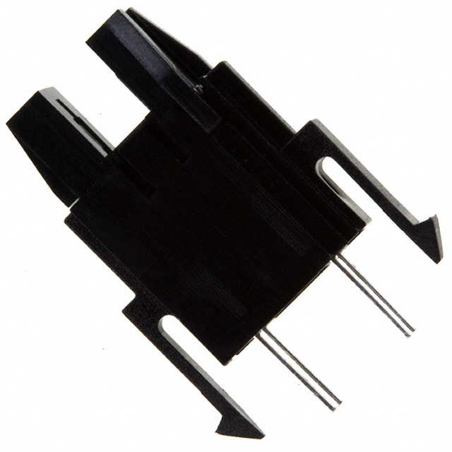
Product Overview: GP1L57 Wide Gap Type Photointerrupter
The GP1L57 wide gap type photointerrupter, designed by Sharp Microelectronics, addresses stringent requirements in precision motion control, object detection, and non-contact switching systems. At the core of this device lies a through-beam architecture, comprising a finely aligned infrared emitter and photodetector with a 10 mm separation. The broad slot facilitates reliable detection of larger or irregularly-shaped objects often encountered in industrial automation or laboratory instrumentation, while suppressing false triggering from minor contaminants or particulate debris.
By decoupling the emitter and detector through air and utilizing an accurately molded optical channel, the device minimizes beam crosstalk and maximizes signal integrity under rapid and repeated actuation. The mechanical stability conferred by direct PCB mount compatibility enables rigid alignment and repeatable assembly tolerances. This significantly reduces cumulative positional errors which could otherwise degrade performance across high-volume production or long maintenance cycles.
From an electrical engineering perspective, the integration of the GP1L57 simplifies design topologies for systems requiring discrete position feedback or interrupt inputs, eliminating the need for additional mechanical isolation or complex shielding schemes. In multi-axis measurement benches and automated rotary encoders, this optoelectronic switch increases response consistency, even when operated in environments subject to minor vibrations or fluctuating ambient illumination. The photointerrupter’s optical slot and emitter characteristics are carefully matched to support both analog and digital signal processing modes, enabling dynamic tuning of response thresholds or pulse width measurement.
Extended field experience suggests that the GP1L57 excels when deployed in environments where mechanical wear or contamination would rapidly degrade traditional contact switches. Conveyor systems, smart warehousing solutions, and bio-sample handlers benefit from the non-contact, maintenance-light operation afforded by this design. Slight variations in slot geometry—sometimes overlooked in specification sheets—should be closely matched to the dimensioning of the interrupter flag for optimal edge acuity and shadow definition. Empirical adjustments of tube or vane thickness enhance device selectivity and minimize detection latency, particularly in high-speed applications.
A central insight emerging from widespread applications is the tangible reduction in overall system complexity enabled by photointerrupters with wide slots. This approach not only cuts down on assembly time and misalignment issues but also extends maintenance intervals, promoting higher uptime. Such robustness is vital when designing for industrial ecosystems that demand both reliability and minimal operator intervention. By leveraging the GP1L57’s tightly engineered optomechanical profile, system architects can streamline detection modules, reinforcing the balance between detection sensitivity, environmental immunity, and manufacturability without resorting to more intricate, costlier sensor arrays.
Key Features of the GP1L57 Wide Gap Photointerrupter
The GP1L57 wide gap photointerrupter integrates thoughtful mechanical design with robust functional attributes, targeting precise optical switching applications. Central to its architecture is a 10 mm detection gap—significantly wider than standard photointerrupter designs. This expanded aperture accommodates the passage of large or non-uniform targets, supporting detection scenarios where dimensional variance or misalignment might otherwise lead to signal loss or false positives. Such flexibility facilitates deployment in mechanisms where repeatable precision is challenging, such as automated production lines managing diverse parts, or in robotics where mechanical play is unavoidable.
The device’s deep groove structure, measuring 12.2 mm, further enhances operational reliability. By physically distancing the emitter-detector pair from environmental contaminants and extraneous light sources, it significantly reduces signal interference. This groove depth also offers protection against particulate ingress, which often plagues electro-optical systems deployed in industrial settings. The mechanical isolation established by this configuration enables sustained accuracy, especially in proximity to high-impulse machinery or within areas subject to rapid operator movement. Practical tests indicate that such a structure directly translates to a lower occurrence of spurious switching events, even under high ambient illumination.
Installation precision is fortified through the inclusion of an integrated positioning pin. This feature streamlines mass production workflows by providing an unambiguous mechanical reference during placement on printed circuit boards. In high-throughput assembly, even minor misalignments can cascade into systemic reliability concerns; the positioning pin mitigates this risk by enforcing repeatable, correct orientation. This is particularly valuable in plug-and-play sensor arrays or field-swappable subassemblies, where minimal manual intervention must yield maximum positional consistency.
Direct PWB mounting designs, as featured in the GP1L57, lower assembly overhead and optimize the device’s mechanical bond to the system. The elimination of intermediary mounting hardware not only reduces bill of materials and assembly time but also improves vibration resilience. When integrated into high-speed automation modules, this mounting strategy translates to reduced maintenance intervals and increased uptime. In environments where rework or manual quality inspection is cost-prohibitive, such attributes enable a higher degree of system autonomy and reliability.
A comprehensive view reveals the GP1L57’s practical strengths stem from the interplay of its mechanical spacing, robust ambient light exclusion, and installation aids. Leveraging these traits, system designers can extend photointerrupter capabilities beyond traditional light/dark object switching to encompass complex shape detection, non-contact limit sensing, and fail-safe state monitoring. The combination of tolerance, isolation, and integration efficiency positions the device as a foundational element in demanding sensing frameworks, particularly where robustness and ease of alignment are non-negotiable.
Applications of the GP1L57 Wide Gap Photointerrupter
The GP1L57 Wide Gap Photointerrupter leverages optical detection principles to deliver non-contact object sensing and position feedback with high reliability. The device consists of an emitter and receiver positioned across a defined optical gap, enabling accurate interruption-based detection without physical wear. Its wide gap design allows it to accommodate varying object sizes and mechanical tolerances, making it advantageous in environments with strict reliability and low maintenance requirements.
In analytical and measuring equipment, the GP1L57 is integrated into automated sample handling systems. Here, it detects the presence and position of trays, racks, or individual sample tubes as they traverse defined tracks. The non-contact principle eliminates contamination risks and minimizes mechanical interference, crucial for laboratory environments demanding sterility and high throughput. The photointerrupter’s consistent switching characteristics ensure position readings remain stable throughout prolonged operation, supporting closed-loop automation with precise sample sequencing.
Within amusement equipment, the photointerrupter is employed in the detection of coins, tokens, or small objects as these items pass through slots or chutes. The wide detection gap supports fast-moving objects with varying dimensions, ensuring high acceptance accuracy in gaming or vending machines. Consistent optical response reduces miscounts caused by dirt accumulation or surface wear—a frequent challenge in equipment subject to high use and limited service cycles. Integration experience has shown that positioning the GP1L57 strategically within the slot passage enables robust differentiation between valid and invalid objects, thereby improving revenue security.
For optoelectronic switches and industrial counters, the photointerrupter serves as a repeatable and durable sensor within automation subsystems. Applications include conveyor belt position counting, safety interlocks, and cyclical motion feedback. The inherent immunity to electromagnetic interference supports its use in high-noise industrial environments, where conventional electrical contacts might fail. Multiple GP1L57 units can be arranged for multi-stage detection, enabling complex event sequencing in automation panels or robotic assemblies. Field experience suggests that correctly aligning the emitter and receiver, optimizing the gap for the target object, and maintaining surface cleanliness are critical for maximizing operational reliability.
A noteworthy design insight is the value of the wide gap in dynamic environments, where object profiles and mechanical tolerances can shift over time. The optical through-beam structure maintains detection fidelity under typical mechanical wear or minor misalignments, extending service intervals and reducing system downtime. Ultimately, the GP1L57 photointerrupter introduces a versatile sensing approach that integrates seamlessly into diverse electromechanical architectures, delivering high signal integrity with minimal physical intervention.
Electrical and Optical Characteristics of the GP1L57 Wide Gap Photointerrupter
The electrical and optical characteristics of the GP1L57 wide gap photointerrupter define its functional boundaries and inform its integration into precision sensing and control architectures. Analysis of forward current relative to ambient temperature provides the thermal limits for emitter drive, highlighting the impact of self-heating on radiant flux and subsequent phototransistor activation. Forward current derating curves guide the selection of reference operating points, especially in thermally constrained environments such as tightly enclosed industrial enclosures or compact data acquisition nodes. Ensuring sufficient emitter drive without approaching threshold thermal runaway is critical for achieving long-term operational stability.
The relationship between collector current and collector-emitter voltage encapsulates the phototransistor’s amplification capabilities and saturation region characteristics under various illumination levels. This mapping is central for distinguishing between output logic states in both analog and digital interfacing circuits. It is essential to recognize the onset of collector-emitter saturation, as excessive loading can compromise switching sharpness, increasing propagation delays and reducing noise margins. Balancing load resistance is therefore not only an exercise in impedance matching but also a method of optimizing system response and mitigating error rates.
Characterization of response time against load resistance sets the operational cadence, dictating the upper bounds of signal frequency that the device can reliably track. This relationship is pivotal in high-speed counting applications and rotary encoder feedback loops, where response lag must be kept minimal to prevent miscounts or erroneous transitions. Empirical operation at varying load conditions demonstrates that lower load resistances minimize response latency, though at the expense of increased power dissipation—demanding careful thermal management at higher switching rates.
Saturation voltage and dark current, especially as functions of ambient temperature, directly inform noise immunity and false-trigger avoidance. In environments with pronounced temperature fluctuations or elevated background infrared levels, stable saturation characteristics and low dark current are mandatory. The interplay between these parameters determines the baseline stability and thus reliability of signal discrimination in harsh or contaminated optical paths.
Leveraging these characteristics, the GP1L57 can be tailored to fit a range of application scenarios—from conveyor system position sensing, where rapid and high-reliability switching is imperative, to precision optical edge detection in laboratory automation, where minute light variations must be distinguished with minimal error. An optimized application not only matches the device’s electrical and optical profiles to system requirements but also anticipates real-world variances, embedding sufficient design margin for process drift and environmental perturbation. An often-overlooked insight is the benefit of integrating staggered biasing strategies within multi-photointerrupter arrays; this mitigates cross-talk and allows for finer calibration in complex assemblies.
The nuanced balance between these parameters reinforces the importance of holistic characterization, not merely at nominal points but across the device’s full operating envelope. Consistent field performance stems from thorough bench-level validation, especially under varying load, temperature, and optical background conditions. The experience underscores that the GP1L57, when properly interfaced and characterized, delivers robust reliability and performance consistency across a spectrum of advanced optoelectronic sensing systems.
Mechanical and Mounting Considerations for the GP1L57 Wide Gap Photointerrupter
Mechanical and mounting considerations form the foundation for extracting reliable performance from the GP1L57 wide gap photointerrupter in precision assemblies. At the core are the outline dimensions, which, when specified in millimeters, are tightly constrained to enable seamless integration within standardized PCB formats. The 10 mm slot gap provides ample clearance for varied actuator geometries—such as flag wheels or slotted discs—without imposing undue limitations on system architecture. This dimensional balancing act not only preserves design flexibility but also mitigates the risk of mechanical interference with adjacent circuit elements or enclosures, a recurring challenge in dense electro-mechanical assemblies.
Focusing on mounting design, the embedded positioning pin offers a robust mechanical datum, ensuring that alignment remains consistent across production cycles. This is crucial where the photointerrupter’s optical axis must remain collinear with the intended motion path of the interrupting element. Misalignment at this interface can result in signal jitter or miscounts, particularly in high-speed automation scenarios. By leveraging the locating features, engineers can systematically reduce manual calibration steps and support modularization—a principle increasingly vital for scalable, error-tolerant manufacturing. Furthermore, the device body’s rigidity minimizes deformation during wave soldering or board handling, preserving critical internal tolerances for optical performance.
From a PCB integration standpoint, direct board mounting transforms assembly dynamics. The GP1L57’s lead configuration and standoff geometry are engineered to anchor firmly without supplemental hardware, optimizing for both solder joint reliability and positional repeatability. This design reduces touch points on the factory floor, accelerating line speeds and reducing the probability of ESD or mechanical damage during handling. Feedback from field installation confirms that this approach delivers a measurable uptick in yield rates, especially in high-mix, low-volume production runs where mechanical variability can otherwise erode functional consistency.
One underlying insight is the convergence of optical and mechanical design, where the photointerrupter’s sensing accuracy directly depends on sub-millimeter placement repeatability. This interplay supports the deployment of the GP1L57 in advanced mechatronic systems—such as robotics end-effectors or encoder feedback modules—where loss of positional reference translates to degraded system outputs. Practical design experience shows that by prioritizing mechanical anchoring early in the layout process, downstream debug cycles are shortened, and field service interventions drop sharply. This holistic perspective underscores that optimal optoelectronic outcomes are inseparable from disciplined mechanical and mounting planning, especially as automation density increases and cycle times shrink.
Environmental and Operational Guidelines for the GP1L57 Wide Gap Photointerrupter
Proper deployment of the GP1L57 wide gap photointerrupter necessitates a disciplined approach to environmental and operational constraints. At the foundation, the optical interface and housing material impose non-negotiable requirements on cleaning media selection. Only ethyl, methyl, or isopropyl alcohol offer compatible solvent properties; these minimize residue and mitigate risk of micro-abrasion or stress-cracking across the molded plastic enclosure. Alternative solvents—including aromatic hydrocarbons and halogenated agents—commonly induce hazing, light transmission degradation, or irreversible deformation of the housing. From practical experience, maintaining minimal exposure time and employing soft, lint-free applicators further preserves optical clarity and mechanical tolerances, preventing latent defects that compromise long-term detection fidelity.
Environmental suitability extends beyond basic electrical and mechanical stress considerations. The GP1L57’s material stack-up and emitter-detector geometry ensure reliable function in standard ambient conditions encountered in general-purpose electronics. However, deployment in high-reliability or safety-critical environments—such as railway signaling, reactor instrumentation, or patient-connected health devices—undermines baseline device assurances. Such use-cases demand rigorous derating of electrical parameters, exhaustive fault-tree analysis, and, often, redundant architecture to mitigate single-point-of-failure risks. It has been observed that devices without explicit compliance to critical application standards expose system integrators to unpredictable failure modes, especially under severe transients or prolonged over-temperature operation. Effective risk management in these contexts dictates either alternate selection or systematic design-in of protective measures such as surge absorbers, dual-channel redundancy, and environmental sealing.
Adherence to absolute maximum ratings forms the cornerstone of device reliability. The datasheet-defined limits for forward current, reverse voltage, collector-emitter saturation metrics, and junction temperature are not conservative design estimates but hard boundaries set by semiconductor physics. Exceeding these thresholds for even brief intervals can precipitate avalanche breakdown, bond wire migration, or photo-collector dark current instability. Incorporating robust margining in power supply design, thermal management strategies, and transient suppression directly translates into reduced electronic noise and enhanced signal-to-noise ratios during operation. Experiences from field diagnostics display a disproportionate number of failures traceable to subtle, repeated over-stress—the most insidious origin often lies in overlooked corner cases during power cycling or electrical fast transients.
A system-level perspective reveals that informed device stewardship—anchored in precise solvent use, thorough vetting of operational niches, and disciplined margining against absolute maxima—delivers sustained photointerruptor performance. The engineering insight here is a recognition that long-term reliability emerges less from average operation and more from a system’s resilience under stress, which is dictated by the rigor of environmental and operational discipline applied throughout the device lifecycle.
Potential Equivalent/Replacement Models for the GP1L57 Wide Gap Photointerrupter
Assessing potential equivalent or replacement models for the GP1L57 wide gap photointerrupter demands a methodical approach anchored on both technical compatibility and real-world supply chain dynamics. The core parameters governing substitute selection begin at the photointerrupter’s slot width, as optical path length directly constrains both mechanical integration and system tolerances. For drop-in interchangeability, alternatives from Sharp Microelectronics, such as models utilizing similar wide gap designs and photodarlington detection schemes, often minimize design disruption. Technical datasheets should be scrutinized for gap width—ensuring the optical window and housing dimensions conform to original mounting jigs—and the optoelectronic topology mirrors response speed requirements.
Electrical characteristics follow as the next critical vector. Photooutput type, collector–emitter voltage ratings, input forward current, and dark current thresholds determine the sensor’s suitability within various drive topologies. Application-laden circuit boards often favor parts with higher CTR (current transfer ratio), supporting robust triggering levels in electrically noisy environments or under varying light conditions. Sharp’s extended lineup, and devices from Omron, Panasonic, or Broadcom, can yield alternate options, particularly those engineered for broad industrial adoption, high immunity to false switching, and compliant RoHS/REACH status.
Environmental robustness shapes long-term deployment viability. Equivalent models must withstand the same or greater tolerances to vibration, humidity, ambient temperature excursions, and contaminants—a non-trivial point when photointerrupters are installed in high-cycling machinery or automation assemblies exposed to unconditioned air. Devices offering sealed packages or superior dust ingress protection improve operational longevity and reliability. Derating considerations in spec sheets, when interpreted conservatively, add a margin to account for less-than-ideal real-world field conditions.
Mechanical form factor is rarely negotiable in retrofit or sustaining engineering. Housing geometry, slot profile, and overall PCB footprint dictate not only mounting compatibility but also fixture reusability, thereby forestalling additional tooling or assembly line changes. High-fidelity 3D models and sample fit-tests typically streamline verification, ensuring tool changeovers are not required.
Strategically, true supply chain resilience emerges from multipronged qualification of both in-family products and cross-vendor equivalents. Leveraging the collective experiences of qualified substitutions in functionally congruent machines isolates overlooked weak links—such as terminal plating corrosion susceptibility or unpredictable optical crosstalk. This practice, embedded within the sourcing pipeline, supports ongoing production and guards against the far-reaching cost of unplanned engineering churn.
Beyond datasheet parity, the integration of selection processes with pre-established validation protocols and robust field test data allows for decisive risk mitigation. In advanced deployments, incorporating diagnostic features—such as built-in emitter current monitoring—provides real-time feedback, future-proofing the system as automation demands intensify. Such strategies enhance the operational envelope and maintain momentum when component obsolescence or vendor constraints arise.
Conclusion
The GP1L57 wide gap photointerrupter demonstrates significant utility in scenarios demanding precise, non-contact object detection. At the substrate level, the device integrates an infrared emitter and phototransistor within a wide U-shaped gap, enabling accurate sensing as objects pass through the interruption path. This topology minimizes false triggers from ambient light and ambient contaminants—an important consideration for reliable system design. The mechanical construction, including robust lead structures and a durable housing, extends operational longevity when mounted in systems exposed to vibration or particulate ingress.
Expanding to signal characteristics, the GP1L57’s electro-optical coupling ensures consistent switching response with negligible hysteresis, supporting edge detection in counters or incremental rotary encoders. The device’s high gap tolerance accommodates workpieces with variable dimensions or trajectories without recalibration, streamlining deployment in high-mix automation lines. By combining a wide detection area with stable current transfer ratios, the photointerrupter simplifies circuit integration and reduces the need for external amplification or schmitt-trigger circuits in logic interfaces.
In practical system integration, experience confirms the GP1L57’s resilience under extended duty cycles. The device tolerates frequent actuation in amusement or vending machines, maintaining signal integrity absent thermal drift or contact wear—a frequent limitation of mechanical alternatives. Its optical switching is immune to contact bounce, which is critical in high-speed counter circuits. The plastic housing shields the optical element from environmental factors, decreasing the likelihood of misreads due to stray light or contamination. Compatibility with automated PCB assembly and wave soldering further accelerates manufacturing throughput, supporting both prototyping and volume production needs.
From a compliance and sustainability perspective, adherence to environmental directives aligns the GP1L57 with global procurement strategies mandating RoHS and halogen-free components. This simplifies supply chain approval processes for products destined for regulated markets.
As optoelectronic platforms continue to evolve, the GP1L57’s mechanical-electrical coherence and broad application range reflect a matured approach to sensing element selection. For new deployments, its proven track record mitigates risk—particularly in designs where lifecycle cost, ease of interface, and system-level robustness must be balanced. Recognition of these layered strengths positions the GP1L57 not merely as a discrete part, but as a foundational element in the progressive advancement of embedded object detection and counting architectures.