 >
>


Product Overview: LMV393DMR2G General Purpose Comparator
The LMV393DMR2G is a dual-channel general-purpose comparator IC engineered for low-voltage operation while maintaining precise signal discrimination. Leveraging CMOS process technology, it supports supply voltages from 2.7 V to 5 V, making it ideally suited to compact and power-sensitive applications, such as portable instrumentation, embedded control, or signal conditioning in wireless nodes. This voltage range aligns well with prevalent logic levels in modern systems, streamlining integration into mixed-signal environments.
The functional architecture centers on two independent comparator channels. Each features low input bias currents and minimal offset voltage—parameters that prove essential when interfacing with high-impedance or low-level analog sources. The rail-to-rail input capability extends design flexibility, permitting accurate threshold crossings near end-of-rail supplies, even as battery voltages sag toward minimum operational levels. Such attributes are leveraged in designs where maximizing dynamic range or supporting low-voltage referencing is required, such as threshold-based battery management or overload protection circuits.
Externally, open-drain outputs facilitate adjustable logic levels through user-defined pull-up resistors. This characteristic confers interoperability with a range of logic families or enables novel wired-AND signaling topologies in multi-source event detection. The negligible supply current per channel further positions the device for deployment in always-on signal path monitoring, supporting aggressive power budgets. Experiences from dense analog front-end layouts demonstrate that the LMV393DMR2G’s compact Micro8 footprint and minimal external component requirement can lead to significant PCB area savings without compromising analog or digital performance criteria.
Noise immunity, propagation delay, and crossover behavior often define comparator usability in precision measurement or rapid event detection schemes. The LMV393DMR2G offers a balanced trade-off, supplying sufficiently fast response for multi-kilohertz signals typical of motion detection or supervisory circuits while maintaining controlled output edges that minimize susceptibility to parasitic oscillation or transients in cluttered board layouts. Field data from safety interlock and alarm systems validate these features, noting stable operation across wide temperature swings and voltage fluctuations.
A key insight for system architects lies in exploiting the device’s dual channel structure for differential thresholding or simultaneous redundant monitoring. This approach bolsters fault tolerance and enables cross-verification without increase in component count, a recurring requirement in industrial or automotive subsystems where reliability per square millimeter is paramount. Moreover, by choosing common reference rails and tight PCB routing, designers can miniaturize analog subsystems while reducing aggregate noise pickup—a technique that enhances reliability in environments with substantial electromagnetic interference.
Integrating LMV393DMR2G comparators with edge conditioning elements, such as hysteresis via positive feedback, transforms the device into a versatile analog-to-digital transition element. This hybrid use case expands the role of a standard comparator from mere state detection to nuanced waveform shaping or frequency discrimination, often seen in low-power sensor interfaces and adaptive signal monitoring cores. Through careful application of these comparatively simple yet robust design principles, the LMV393DMR2G positions itself as a foundational building block in the architect’s toolkit, bridging traditional analog signal domains with emerging low-voltage digital processing engines.
Key Features and Performance Highlights of LMV393DMR2G
The LMV393DMR2G dual comparator integrates an array of features engineered to facilitate efficient analog signal comparison within compact and energy-sensitive systems. Its electrical characteristics are optimized for both versatility and robustness, targeting portable equipment and general-purpose circuitry where design constraints demand both high integration and low power budgets.
Supporting guaranteed operation at supply voltages of 2.7 V and 5 V, the LMV393DMR2G enables seamless adaptation to both low-voltage digital platforms and legacy 5 V architectures. This dual-rail compatibility not only broadens application reach across mixed-signal environments but also streamlines inventory and design cycles when interoperability is required. The input common-mode voltage extending down to ground level is particularly relevant for single-supply topologies. This capability simplifies reference generation and maximizes usable input dynamic range, facilitating precision at low signal levels without the complexity of negative supply rails or additional biasing.
The open-drain output configuration is a deliberate design strategy, yielding significant flexibility in logic interface. By allowing external pull-up selection, designers can fine-tune logic thresholds for direct compatibility with microcontrollers, FPGAs, or custom bus voltages. The configuration also supports wired-OR logic structures, instrumental in status flagging, fault aggregation, and distributed monitoring systems. Integration into I2C or similar bus arbitration schemes benefits from this flexible logic-level tailoring, reducing the need for translation circuits and simplifying PCB layout.
Low quiescent current, specified at typically 60 µA per channel at 5 V, translates directly into extended battery life and reduced thermal loading—core considerations in portable instrumentation and always-on monitoring nodes. This is achieved without compromising performance metrics critical to responsiveness. The typical output saturation voltage of 200 mV at 5 V ensures strong low-level logic assertion even with moderate sink currents, preventing erroneous state detection in noisy environments or with higher capacitance loads. In practical PCB deployments, this contributes to consistent logic integrity across temperature and supply variations, reinforcing system-level reliability.
A propagation delay in the vicinity of 200 ns at 5 V empowers the LMV393DMR2G for real-time control loops, fast window detection, digital pulse shaping, and safety-interlock functions where decisive comparator actions impact system stability or fault reaction time. Circuits requiring tight timing, such as clock edge sampling and burst-mode communications, benefit from this expeditious signal discrimination. The delay behavior remains predictable across supply and temperature gradients, preserving deterministic operation—an inherent advantage for embedded control reliability.
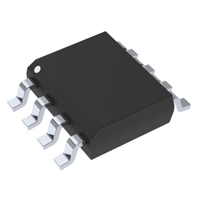
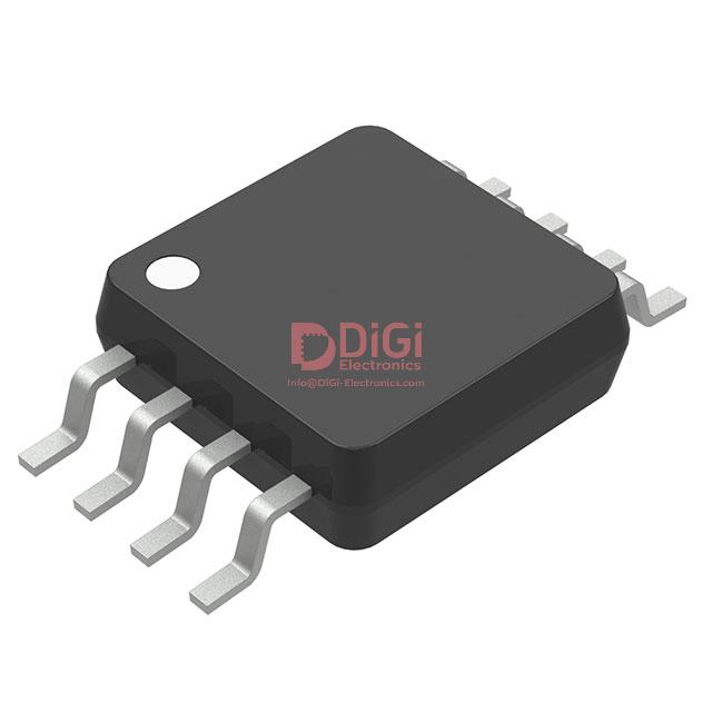
Package diversity, including 8-MSOP (Micro8), SOIC-8, and UDFN8 options, addresses both board-density and thermally constrained scenarios. The MSOP footprint is especially effective for space-constrained modules, while the UDFN variant enhances heat dissipation in surface-mount assemblies with elevated current densities. Matching package selection to deployment context streamlines the realization of compact, durable assemblies without sacrificing access to industrial-grade device variants.
For deployment in automotive, industrial, and high-reliability sectors, the LMV393DMR2G family offers AEC-Q100 qualified options, underlining operational confidence in electrically and environmentally hostile settings. This qualification aligns with stringent OEM validation workflows, allowing for seamless drop-in replacement during design maintenance or lifecycle extension initiatives.
Sophisticated analog front-ends leverage the LMV393DMR2G for voltage monitoring, window detection, and brownout-protection schemes, where consistent threshold response and low power are paramount. Through open-drain versatility and single-rail friendly inputs, system integration is simplified, supporting streamlined BOM profiles and predictable manufacturing outcomes. Integrating these comparators early in systems with fluctuating supply rails or multiplexed analog domains circumvents the pitfalls of over-engineered compensation or unnecessary analog complexity, underscoring the value provided by the LMV393DMR2G’s feature-rich architecture.
Electrical Characteristics and Typical Performance Parameters of LMV393DMR2G
The LMV393DMR2G is a dual low-voltage comparator engineered for robust performance across both 2.7 V and 5 V power rails, accommodating mainstream digital and analog system requirements. Its design provides stable operation in environments ranging from -40°C up to 85°C, maintaining predictable behavior even as supply and ambient conditions fluctuate. For automotive or industrial applications subject to harsher environments, extended temperature variants such as the NCV393 operate reliably up to 125°C, leveraging identical silicon-level mechanisms for temperature resilience.
Analysis begins at the quiescent characteristics: the typical supply current of approximately 60 µA per channel at 5 V signifies low static power consumption—a key factor in battery-powered or always-on systems where total load must be minimized. This efficiency is achieved without compromising dynamic response or comparator accuracy.
At the input stage, the common-mode voltage range stretches from the negative rail (ground) up nearly to the positive supply, only falling marginally short of full-rail input for signals near Vcc. This nearly rail-to-rail operation supports flexible interfacing with diverse input signals, enabling both ground-sensing and top-of-rail monitoring in mixed-signal environments. Empirically, the input offset voltage remains within bounds sufficient for typical analog sensing and zero-crossing determinations, minimizing calibration complexity even as boards age or environmental exposures vary. The ESD protection circuitry protects during hot swapping and assembly phases, reducing latent failure rates that stem from inadvertent discharges, an often-underestimated risk in rapid prototyping environments.
The output stage exploits an open-drain architecture, decoupling the output logic level from the comparator’s own supply voltage. This design supports seamless integration with logic circuits operating at different IO voltages—an important distinction in heterogeneous designs where interfacing across legacy and modern nodes is common. The correct sizing of the external pull-up resistor is crucial; experience indicates that values between 2 kΩ and 10 kΩ balance switching speed and power dissipation, though application-specific tuning may be required to suppress unwanted noise pickup or reduce output rise times.
Switching performance is characterized by stable, clean transitions with minimal oscillation or chatter at the threshold, particularly when a modest overdrive is present between the input voltages. In practical deployments such as voltage monitoring or window comparator circuits, this translates to reliable state transitions even in the presence of analog noise, supporting both signal conditioning and digital logic handoffs without excessive filtering. The device’s internal architecture minimizes propagation delay variance with temperature and supply, reducing timing uncertainty in clock-sensitive or feedback-type implementations.
Consideration should also be given to PCB layout practices. Short, direct routing at the comparator’s inputs, along with strategic ground referencing, further mitigates susceptibility to spurious triggers, an aspect underscored when deploying in high-EMI industrial settings. The LMV393DMR2G’s solid ESD resilience and low output saturation voltage—200 mV typical at 4 mA sink current—ensure compatibility with direct drive of optoisolators and discrete logic gates where budgeted headroom for logic lows is limited.
The essential insight underlying optimal use of the LMV393DMR2G lies in its balance of efficiency and interface agility. Its parameter profile facilitates not just low-power design but also robust, predictable analog-to-digital interfacing under diverse electrical and environmental conditions. This versatility, paired with careful supporting circuit design and external component selection, enables reliable deployment in instrumentation, supervisory, and signal-level detection roles, both as a core element and as a glue logic solution bridging analog and digital domains.
Package Options and Mechanical Details for LMV393DMR2G
LMV393DMR2G packaging strategy targets both spatial optimization and environmental compliance, addressing the diverse needs of modern electronics. Its Micro8 (8-MSOP) format, characterized by a highly compact outline, is engineered for applications demanding aggressive board space minimization. This configuration especially benefits battery-powered handhelds and modular sensor arrays, where PCB real estate directly translates to product competitiveness. The use of case 846A ensures interoperability with automated pick-and-place equipment, and exacting lead coplanarity specifications minimize open connections during reflow, reducing field failure rates.
The SOIC-8 variant, leveraging case 751, presents a balance between manufacturability and robustness. Its slightly larger dimensions favor designs in industrial controls and process instrumentation where ease of manual inspection and higher tolerance for mechanical stress are critical. The wider lead pitch reduces solder bridging defects during wave soldering, a recurring practical concern in high-throughput assembly lines. This form factor’s adoption is further bolstered by its predictable thermal profile during soldering, simplifying process window control and reducing susceptibility to thermal-induced warpage, especially in multi-layer PCBs with heavy copper pours.
UDFN8, based on case 517AJ, fulfills requirements for ultra-thin and low-profile integrations. This package is optimized for mobile and wearable electronics, supporting stacked or double-sided placement and enabling tighter component clustering. Its minimized z-axis height limits potential interference in high-frequency signal paths, which becomes critical in mixed-signal environments or RF front-ends. The exposed thermal pad enables efficient heat dissipation despite size constraints, enhancing long-term device reliability under continuous operation.
Across all package variants, strict adherence to JEDEC mechanical outlines guarantees process compatibility and reduces NPI risk when migrating between suppliers or manufacturing sites. Precise dimensional tolerances support high-speed, automated SMT processes, maximizing yield through repeatable component registration and solder joint integrity. RoHS compliance, Pb- and halogen-free construction, and compatibility with lead-free solder profiles permit unrestricted application in global markets and future-proof designs against evolving environmental mandates.
Optimized recommended footprints, validated through actual assembly and inspection processes, balance solder paste volume with pad-to-lead alignment, ensuring strong joints while simplifying rework. These layout guidelines, when adhered to, mitigate common pitfalls such as tombstoning or cold solder defects and streamline production ramp-up for new designs. The LMV393DMR2G’s flexible package ecosystem, combined with rigorously engineered mechanical details, offers a comprehensive platform—supporting rapid prototyping, scalable manufacturing, and mission-critical deployment across the spectrum from consumer gadgets to industrial infrastructure.
Application Guidelines and Circuit Design Considerations Using LMV393DMR2G
The LMV393DMR2G is engineered for flexible integration into analog signal comparison tasks, serving in roles such as voltage level indication, window discrimination, zero-crossing detection, and battery status monitoring. The device leverages an open-drain output architecture, obligating designers to select appropriate pull-up resistors, typically within the 1 kΩ to 10 kΩ range. This choice is a critical intersection: lower resistor values optimize transition sharpness and propagation delay, enabling crisp digital edge formation at the cost of increased static power consumption during logic-low states, while higher values favor energy efficiency yet may compromise switching acuity in high-speed or capacitive environments.
Effective obstacle remediation within comparator circuits centers on noise resilience and input stability. Hysteresis integration, implemented via external resistor networks, addresses the phenomenon of output oscillation when the input voltage hovers near the comparison threshold or exhibits gradual transitions. Selection between inverting or non-inverting hysteresis feedback topologies should be determined by application-specific constraints—such as desired polarity of switching and coupling to neighboring analog domains. Empirical tuning of hysteresis resistor values in the prototyping phase is indispensable, offering a pragmatic route to suppress transient noise and ensure deterministic behavior in production environments subject to fluctuating analog sources.
Unused comparator channels in dual or quad packages present potential for latent instability if inputs are left floating. Driven termination—assigning one input to VCC and the other to ground—eliminates spurious toggling, mitigating risks of extraneous power draw and electromagnetic interference propagation. In system layouts characterized by dense analog and digital cohabitation, this simple tie-off protocol yields outsized benefits in ensuring comparator subsystem tranquility and facilitating straightforward manufacturing test procedures.
Application of LMV393DMR2G extends notably into battery management schemas, where the comparator efficiently classifiers voltage thresholds for charge state indication or automatic cutoff circuits. In portable device design, such as notebooks and PDAs, the device underpins signal conditioning chains that translate analog sensor outputs into robust digital triggers, harmonizing disparate voltage domains and immunizing logic states against ambient artifacts. Its use for straightforward analog-to-digital thresholding expedites rapid prototyping; the open-drain topology dovetails with a variety of microcontroller and FPGA logic levels, eliminating inter-level contention.
Layered design principles emphasize that optimal performance is not contingent on individual component choice alone, but on holistic evaluation of environmental noise profiles, targeted switching speed, input signal variability, and system-level interfacing voltages. Practical deployments demonstrate that methodical selection of resistor values in hysteresis and pull-up circuits, coupled with disciplined channel termination strategies, are decisive in achieving consistent, low-latency, and noise-immune operation. Implicit in such implementations is the recognition that comparator circuits must be engineered as adaptive subsystems, rather than static modules, with component selection dynamically referenced against evolving application constraints and field performance feedback.
Potential Equivalent/Replacement Models for LMV393DMR2G
The task of identifying potential equivalent or replacement models for the LMV393DMR2G centers on understanding both the circuit-level implications and the procurement strategy. The LMV393DMR2G, a dual comparator, is part of a broader product family differentiated primarily by channel count, packaging, and specialized features. The LMV331 presents itself as a single-channel counterpart, particularly effective in designs where board area is highly constrained or where a single comparison node suffices. For designs scaling up in channel requirements, the LMV339, with its quad-channel configuration, offers an efficient route to minimize component count, streamline layout, and potentially reduce BOM complexity.
Assessment of replacements extends beyond surface compatibility. The NCV331 introduces automotive-focused attributes, such as an extended operating temperature up to +125°C and compliance with AEC-Q100 standards, making it ideal for harsh environments or applications requiring rigorous reliability verification. Its feature set enables seamless integration into automotive or industrial systems where certification is non-negotiable.
In practice, the interchangeability of these comparators is contingent on a meticulous review of their electrical parameters. Key metrics such as input offset voltage, propagation delay, and supply current directly impact analog front-end fidelity and response time. A subtle mismatch in these characteristics can adversely affect system stability, noise margin, or power budget—especially in sensitive instrumentation or battery-powered devices. Direct experience highlights that pin-for-pin compatibility, while desirable, is not sufficient; thermal characteristics and PCB footprint compatibility often necessitate additional layout or qualification effort during late-stage engineering changes.
When implementing substitutes, constraints imposed by package variants—such as SOT-23, SOIC, or TSSOP—can affect manufacturability and assembly flow. Engineers routinely benefit from verifying the supplier lifecycle and second-source availability to protect the supply chain against obsolescence or allocation shortages. This proactive strategy mitigates redesign cycles and maintains production agility.
A nuanced perspective reveals that although datasheet parity establishes a baseline, a model’s behavior under real-world transient conditions, such as common-mode range excursions or recovery from saturation, frequently distinguishes a merely equivalent part from a truly drop-in replacement. System verification, preferably under representative load and temperature variation, is indispensable for robust substitution.
Ultimately, a well-executed comparator selection process accounts for operational parameters, system certification needs, supply risks, and practical implementation challenges. Design flexibility is maximized by treating cross-compatibility as a multidimensional problem, integrating both technical and logistical evaluations early in the development timeline. This layered approach ensures enduring performance while maintaining sourcing resilience.
Conclusion
The LMV393DMR2G, produced by onsemi, is engineered to address the nuanced requirements of modern systems operating at reduced voltage rails and constrained power budgets. The core architecture centers on low quiescent current and wide supply range, supporting voltages down to 2.7V while maintaining consistent propagation delay and output integrity. Its input stage features rail-to-rail common-mode capability, ensuring compatibility with a wide spectrum of analog signal paths within battery-powered or energy-sensitive designs. Output stages are tailored for open-drain connectivity, permitting versatile logic-level interfacing and easy integration into mixed-voltage domains.
Industry-standard SOT-23-8 packaging provides a compact solution to board real estate challenges prevalent in highly integrated consumer electronics, wearables, and compact industrial controllers. The mechanical and electrical robustness of the package supports effective automated assembly, repeatable solder joint integrity, and thermal stability under fluctuating environmental conditions.
In practical deployment, the LMV393DMR2G demonstrates resilience in high-noise environments, exhibiting low input offset and high common-mode rejection ratio. This performance translates to stable reference tracking and reliable threshold detection within sensor interfaces, DC/DC converter circuits, and protection modules. Its low-current characteristics extend battery runtime in portable medical sensing or remote IoT endpoints, reducing the need for frequent maintenance interventions.
From a systems perspective, the device’s pin compatibility with legacy comparators simplifies design updates, offering a risk-mitigated migration path when upgrading older platforms to leverage improved efficiency or supply chain flexibility. Compatibility with alternative second-source parts enables streamlined design-in processes and ensures procurement resilience, a critical factor in volume manufacturing cycles.
A careful layout, such as minimizing input trace length and shielding critical nodes, further optimizes the device's performance in precision analog front-ends. In scenarios with stringent board space or power envelopes, de-rating practices and close adherence to recommended operating conditions help sustain long-term device reliability, even under extended operation or rapid switching regimes.
The continuing relevance of the LMV393DMR2G emerges from its synthesis of established analog principles and design refinements aligned with modern deployment contexts. This makes it particularly suitable not merely as a drop-in comparator, but as a strategic element in platforms requiring scalable, reliable analog decision-making within a continually evolving electronics landscape.