>
>


Product overview
The LM393DMR2, a dual independent precision voltage comparator from onsemi, implements a balanced architecture aimed at robust signal discrimination under varied operating conditions. Central to its design is a low input offset voltage, a parameter that directly impacts sensitivity and accuracy when resolving small differential signals. Internally, the comparator leverages input stage topology optimized to suppress offset drift across temperature gradients and supply excursions, maximizing fidelity for analog-to-digital front ends and threshold detection circuits.
Operational efficiency is further enhanced by a broad supply voltage range, accommodating both low-voltage digital logic systems and higher-voltage analog domains typical of industrial sensor arrays. Its minimal quiescent current addresses energy constraints in battery-powered applications, extending device longevity without compromising on responsiveness. This characteristic proves critical during deployment in automotive control modules and embedded diagnostics, where power budget and system stability are closely linked.
Physical integration is streamlined through availability in both Micro-8 and SOIC-8 packages. Their compact form factors simplify PCB layout constraints and enable high-density placement in space-limited enclosures. The LM393DMR2 exhibits rail-to-rail output swing, reducing the need for additional level-shifting circuitry when interfacing with subsequent digital blocks. In field use, its tolerance to input common-mode voltages approaching ground makes it favorable for precision undervoltage lockout and monitoring functions, especially in multi-voltage architectures.
The core design philosophy prioritizes deterministic response in noisy environments. Input filtering minimizes susceptibility to transient spikes, while internal compensation ensures rapid propagation delay without excessive overshoot. Predictable switching characteristics facilitate robust design in mixed-signal environments, supporting high-integrity edge detection and pulse width monitoring.
From a procurement perspective, the LM393DMR2's pedigree within the LM393 family ensures continuity of supply and cross-compatibility across legacy and modern platforms. Built-in reliability features and rigorous qualification support its selection in applications demanding extended operational lifetimes and reduced field failures.
A nuanced aspect of the LM393DMR2's utility is its adaptability: in hands-on prototyping, the device consistently maintains stable thresholds under fluctuating load and bus conditions, reflecting well on its internal matching and noise immunity. This reliability underpins its role across consumer devices, where system calibration requirements vary, as well as within industrial controllers, where uptime and diagnostics are paramount. The LM393DMR2 thus exemplifies a component that integrates foundational analog precision with practical design flexibility, achieving a synthesis of performance and reliability that is seldom compromised.
Key features of the LM393DMR2 dual comparator
The LM393DMR2 dual comparator integrates advanced features, meeting stringent requirements across diverse analog signal processing applications. Its architecture accommodates both single-supply (2.0 V to 36 V) and dual-supply (±1.0 V to ±18 V) environments, supporting compatibility with a broad spectrum of analog and mixed-signal platforms. This flexibility streamlines inventory management in designs that migrate between industrial and portable domains.
Precision in voltage comparison emerges from its low input offset voltage—typically 2.0 mV, with an absolute ceiling at 5 mV. Such minimization of offset ensures high fidelity when resolving millivolt-level differential signals. This is especially critical in sensor front-end circuits and low-level signal discriminators, where even minor offset can mask or distort threshold crossings. Consistent performance is further reinforced by low input bias (25 nA) and offset currents (5 nA), directly reducing static error sources and ensuring stable behavior over extended operational lifetimes.
Current consumption remains a dominant concern in energy-constrained systems. The LM393DMR2’s quiescent current, capped at 0.4 mA, remains largely independent of supply voltage. This trait is leveraged in battery-operated modules or solar-powered monitoring devices where efficiency translates into practical runtime benefits and reduced thermal footprints. Even in high-density assemblies, the comparator’s minimal draw supports aggressive power budgeting without sacrificing speed or responsiveness.
Input common-mode range reaches from ground up to the maximum supply potential in single-supply topologies, eliminating the need for virtual ground references in ground-sensing comparators—essential in zero-crossing detectors, relay drivers, and window comparators for fault monitoring. Its high differential input voltage tolerance, limited only by supply itself, bolsters circuit resilience against transient overdrive conditions—a frequent occurrence in industrial and automotive environments with unshielded wiring and unpredictable signal swings.
The open-collector output design is a critical enabler for logic interface interoperability. Direct connectivity with DTL, TTL, ECL, MOS, and CMOS families supports seamless communication between the analog and digital domains, simplifying interfacing in mixed-signal boards with multi-voltage logic. Open-collector topology also facilitates wire-OR and wired-AND configurations, allowing multiple comparator outputs to aggregate alarms or control lines without external logic.
Robustness is built in: internal ESD clamps suppress fast surges at the input pins, guarding against assembly or field damage and reinforcing long-term reliability. Compliance with environmental regulations (Pb-Free, Halogen Free/BFR Free, RoHS) adds competitive value, easing integration into green-certified product lines and aligning with global supply chain mandates.
In field deployment, the LM393DMR2 demonstrates measurable advantages. Devices leveraging its full input common-mode swing require less external conditioning circuitry. Design cycles are shortened when offset errors and bias currents are negligible, as thermal or device-matching compensations can be deemphasized or omitted. Furthermore, the practical combination of protection features and interface versatility sets the LM393DMR2 apart when scaling designs from prototypes to high-volume production, particularly where failure rates and compliance costs must remain tightly controlled. The underlying design choices consequently yield not only technical robustness but also clear project management and lifecycle benefits, marking this device as a foundation component in modern signal comparison architectures.
Electrical characteristics and performance data for LM393DMR2
Detailed examination of the LM393DMR2’s electrical characteristics reveals a component engineered for robust signal discrimination across diverse environments. At the foundation, the device’s wide operating temperature range responds to various industrial and automotive integration challenges—standard grades maintain function between 0°C and 70°C, while specialized variants cover demands spanning –40°C to +125°C. This versatility ensures reliable threshold detection in temperature-volatile scenarios such as under-hood instrumentation or factory process control, where abrupt ambient shifts would compromise less resilient designs.
Focusing on the output stage, the comparator’s capacity to sink up to 20 mA regardless of supply voltage simplifies output stage calculations and expands its compatibility with TTL and CMOS logic circuits. However, practical designs should avoid prolonged output shorts to VCC, as the lack of automatic current limiting can feed thermal overstress and eventual failure. Correct engineering practice involves series resistance or logic-level signaling to forestall such overstress, embedding these precautions early in schematic capture.
Response dynamics are quantified with a 100 mV input transition and 5 mV overdrive, underscoring the LM393DMR2’s aptitude for detecting fast, low-amplitude signals. In fast comparator applications—such as window detectors or zero-crossing circuits—rapid response directly correlates with timing precision and overall system fidelity. Application experience consistently shows that deliberately increasing the input differential can further shorten propagation delays, an approach often exploited in time-critical analog front-ends. Yet, designers must balance speed benefits against noise immunity, ensuring high-frequency artifacts do not trigger false switching.
The comparator’s overvoltage immunity stems from its input topology, which allows one input to surpass the positive supply rail, provided the opposite input remains within the specified common-mode range. This feature suits scenarios with signal excursions due to coupling or fault transients—such as input channels exposed to unconditioned sensors or noisy transmission lines—allowing for graceful handling of momentary overvoltage events. However, input swings below –0.3 V risk forward biasing internal junctions, making board-level clamping or series resistance mandatory when interfacing with signals prone to negative undershoot.
A central aspect of LM393DMR2’s architecture is its PNP differential input stage. The resulting nearly-constant bias current flows out of the input pins, an important trait when connecting to high-impedance sources. This behavior minimizes input offset drift and provides superior input common-mode performance compared to FET- or NPN-based alternatives. Nevertheless, when bias-sensitive circuitry adjoins the comparator, unaccounted input current can introduce errors—particularly in precision analog measurement systems. Strategic sensor buffering or bias compensation becomes essential, especially in multi-channel analog acquisition.
Within high-reliability applications, these characteristics consolidate the LM393DMR2 as a preferred comparator for signal conditioning, threshold detection, and fault monitoring. A key insight is that successful use depends not simply on specification compliance, but on disciplined consideration of overstress protection, input conditioning, and load matching. Applying these engineering controls fully leverages the LM393DMR2’s strengths while safeguarding operational longevity across deployment contexts.
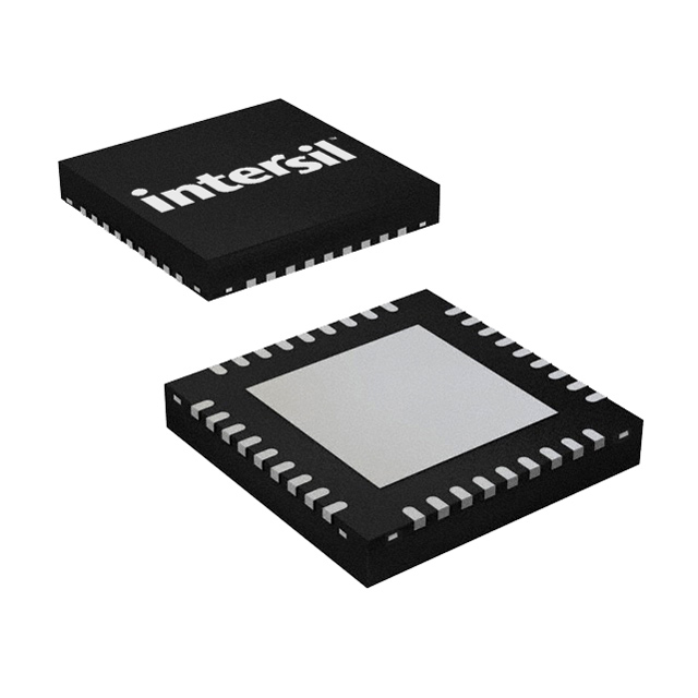
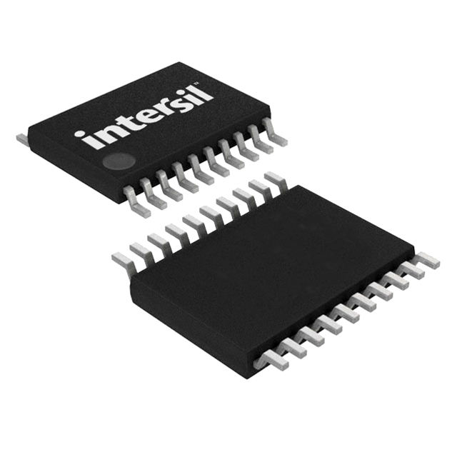
Package options and mechanical dimensions for LM393DMR2
The LM393DMR2 operational amplifier integrates seamlessly into a range of board architectures by offering multiple packaging options optimized for space efficiency and automated manufacturing. The device is available in industry-standard SOIC-8 (Narrow Body) and Micro-8 surface-mount packages. SOIC-8, designed in accordance with JEDEC specifications, ensures reliable alignment with automated pick-and-place systems and supports straightforward reflow soldering. Its consistent lead pitch and narrow form factor enable dense component placement, minimizing routing complexity in multilayer boards. The Micro-8 option provides even greater spatial efficiency, with negligible impact on electrical performance, thus facilitating implementation in miniature assemblies such as sensor modules or wearables.
Mechanical dimensions and land-pattern recommendations are precisely documented in the datasheet, providing dedicated guides for footprint creation in EDA tools. These drawings incorporate tolerances for both package and pin geometry, mitigating risk of solder bridging or open connections. A standardized pin assignment across both package variants streamlines circuit design and enables straightforward substitution, which proves essential in prototyping cycles and volume production transitions.
For traceability and quality assurance, each LM393DMR2 unit features comprehensive package marking according to established onsemi conventions. This embedded identifier, recognizable throughout logistics chains, expedites component verification and ensures compliance with regulatory audits. Field deployment has demonstrated that adopting these standardized markings, in conjunction with automated optical inspection systems, significantly reduces error rates during inbound component verification and assembly validation.
Identification of optimal package selection depends on application constraints. Projects requiring ultra-compact layouts, such as mobile platforms or IoT nodes, benefit significantly from Micro-8's reduced occupancy, improving performance-per-area metrics and enabling advanced device miniaturization. Conversely, SOIC-8's robustness and proven manufacturability make it preferable when balancing cost, compatibility, and assembly yield in high-volume production.
Experience indicates that meticulous adherence to recommended land-pattern geometry and mounting strategies dramatically enhances reflow results and minimizes post-reflow inspection cycles. Proactive engagement with package dimension drawings within the initial PCB design phase reduces downstream revisions and supports first-pass manufacturing success. Integration of the LM393DMR2 with well-established package standards accelerates project timelines and expands flexibility for future design updates. Recognizing the interplay between mechanical footprint, signal integrity, and process compatibility is key to optimizing both electrical performance and manufacturing efficiency in modern analog circuit deployments.
Application considerations for LM393DMR2 in circuit design
The LM393DMR2, a widely utilized dual comparator, distinguishes itself by accommodating a broad supply voltage range and exhibiting stable, low-offset performance, thereby supporting a spectrum of applications demanding precision and noise resilience. Understanding its core functional mechanisms provides the basis for effective deployment in diverse circuit topologies.
Fundamentally, the input structure of the LM393DMR2 supports common-mode voltages extending down to ground, enabling seamless integration in zero-crossing detection schemes. This feature, combined with a typically low input offset voltage, ensures accurate differentiation between signal polarities even in low-amplitude, line-powered environments. For example, in AC phase monitoring modules interfacing with microcontrollers, consistent triggering during signal transitions mitigates false detection events—particularly relevant in noisy mains environments and at low signal levels.
In timing component design, the LM393DMR2’s high open-loop gain and extended bandwidth are leveraged to produce sharp, repeatable output transitions. These characteristics are essential when configuring oscillators or pulse generators where timing accuracy and switching symmetry underpin performance. Feedback-derived oscillators exploit the comparator's clean switching to minimize pulse-to-pulse jitter, translating directly to reliable timing in reference clock or delay generator circuits. In practical implementations, component selection for the feedback and timing networks directly determines frequency stability and response to loading, making layout and parasitic management critical for robust operation.
The integration of hysteresis via positive feedback differentiates the LM393DMR2 in threshold-sensitive applications. With the appropriate resistor network, stable, noise-immune switching is achieved, overcoming traditional comparator vulnerabilities to slow or noisy input transitions. This is particularly valuable in sensor interfacing, where input signals often drift slowly across threshold points, and in windowed comparator circuits designed to detect when inputs enter or exit defined voltage bands. Experience demonstrates that optimizing hysteresis values tailored to expected signal conditions often resolves debounce issues and prevents erratic toggling in high-interference environments.
For control-related implementations in industrial and automotive contexts, the LM393DMR2 maintains compatibility with higher-specification family derivatives, relying on a similar architecture that emphasizes reliability over a broad temperature range. While automotive-grade variants extend qualification margins, careful circuit protection—such as minimizing input pin floating, managing supply transients, and ensuring adequate decoupling—offers substantial improvements in system robustness. Within alarm and monitoring subsystems, the comparator's quick response and immunity to supply variations underpin fail-safe operation, provided classic comparator caveats—like preventing DC output shorts to VCC and controlling output loading—are respected.
Engineered success with the LM393DMR2 depends heavily on mindful design practices. Input resistors should not exceed 10 kΩ to reduce susceptibility to instability from stray capacitance and electromagnetic coupling. All unused comparator inputs must be secured, preferably tied to a known voltage potential, to forestall unpredictable behavior and inadvertent oscillations. Mechanical layout should isolate sensitive analog paths, while outputs must be protected against overcurrent, especially during fault conditions such as accidental output-to-VCC shorts, which pose reliability risks.
A salient insight in deploying the LM393DMR2 is its capacity as a precision component in loosely regulated environments: by strategically leveraging its tolerance to ground-referenced inputs, low offset, and practical frequency response, it can act as a bridge between analog phenomena and digital control, even under less-than-ideal conditions. Well-executed designs often result from harmonizing these core electrical attributes with thorough defensive engineering, translating manufacturer specifications into tangible resilience at the circuit level.
Potential equivalent/replacement models for LM393DMR2
In evaluating functionally equivalent or drop-in replacement options for the LM393DMR2, a methodical approach starts with electrical and mechanical compatibility, then extends toward long-term supply chain resilience and compliance mandates. Among direct replacements, devices such as the LM393E from onsemi deliver closely matched parameters, typically mirroring the input offset voltage, propagation delay, and supply current of the LM393DMR2, but with revisions that can optimize performance for marginally demanding rail-to-rail or temperature-bound applications. Device selection at this level often hinges on the nuances of input bias stability, power supply accommodation, and pin-for-pin interchangeability within the existing PCB footprint.
Broader industrial requirements often necessitate comparators like the LM293 or the LM2903-series, which feature extended temperature ranges and, in some variants such as the LM2903V, additional robustness against voltage transients and output latch-up. The LM293 stretches operational boundaries to –25°C to +85°C, accommodating applications exposed to variable climates or peripheral industrial control. For systems targeting even higher reliability and low failure tolerance—such as automotive ECUs or powertrain management—the NCV2903 distinguishes itself by meeting AEC-Q100 standards and supporting PPAP documentation, ensuring both process traceability and long-term availability under automotive supply agreements.
Selecting among these alternatives involves analysis beyond datasheet tables. Offset voltage stability, input common-mode limits, and output drive capabilities must be quantitatively verified under representative use-case conditions—simulated worst-case temperature drifts, voltage supply sags, and noisy signal environments. During board spin iterations, differences in input offset or response time, even when minimal, can manifest as functional anomalies at system margins. It’s common to iterate through characterization boards with multiple candidate comparators to empirically confirm parametric equivalence and mitigate latent risks, particularly in designs sensitive to window comparator accuracy or jitter in signal edge detection.
Interchangeability sometimes reveals itself in subtle PCB or system-level observations. Slight differences in input bias current or output stage topology can affect pull-up resistor selection or introduce timing glitches, so real-world bench measurements are indispensable. Experience shows that while datasheet figures often align, secondary parameters—EMI immunity, output phase reversal susceptibility, and recovery from fault conditions—can differentiate operational maturity of candidate devices.
A pragmatic insight is the importance of engaging component suppliers early for lifecycle support and revision control, particularly for high-volume or safety-critical builds. Premature obsolescence or uncommunicated silicon revisions have, on occasion, led to costly board requalifications. Incorporating replacement flexibility into BOM strategy—by dual-qualifying two or more pin-compatible comparators—bolsters resilience, reducing vulnerability to market shocks or allocation periods.
In summary, the process of qualifying LM393DMR2 replacements integrates technical diligence with practical supply chain foresight, requiring rigorous verification of critical parameters under actual application stresses, iterative prototyping, and proactive sourcing strategies to ensure uninterrupted and robust comparator performance.
Conclusion
The onsemi LM393DMR2 dual comparator exemplifies a balance of precision and power efficiency, addressing the evolving demands of analog signal comparison in contemporary electronic architectures. Its supply voltage flexibility, spanning a wide range without compromising core performance metrics, ensures compatibility with legacy systems and modern low-voltage designs alike. The device’s low-input offset voltage, achieved through careful internal architecture and process controls, minimizes error propagation in signal conditioning stages. This feature proves crucial in threshold detection circuits, window comparators, and zero-crossing detectors, where accuracy directly influences system reliability.
Further reinforcing its advantage is the LM393DMR2’s minimal quiescent current draw, which enables energy-conscious deployment in battery-powered devices, remote sensors, and distributed control modules—sectors where total power budget is tightly managed. Multiple surface-mount package options expand integration possibilities, supporting high-density PCBs and thermal considerations intrinsic to industrial and automotive environments. The comparator’s open-collector output stage facilitates seamless interfacing with varied logic levels and enables wired-AND configurations, a notable benefit in multi-channel comparison applications or fault detection networks requiring robust logic flexibility.
Effective circuit implementation leverages the LM393DMR2’s high common-mode voltage range and impressive CMRR, allowing for precision performance under noisy or fluctuating supply conditions—a frequent scenario in harsh industrial fields or under-hood automotive control. Transition edge speed and minimal propagation delay further enrich real-world applicability by supporting rapid event detection and time-critical system responses, such as motor protection circuits or supervisor subsystems within embedded controller designs.
Broader component ecosystem support, with readily available drop-in equivalents, allows streamlined sourcing and mitigates risks associated with single-vendor dependency. This aspect is vital for long-life platforms and agile prototyping, where design continuity and component interchangeability accelerate project timelines. In practice, leveraging such feature parity between equivalent models enables designers to maintain tight design cycles, adhere to stringent qualification standards, and ensure supply chain resilience—factors increasingly critical in competitive electronics markets.
Deep integration of the LM393DMR2 in both finished products and rapid proof-of-concept platforms results from its mix of analog finesse and practical engineering forethought. Consistent performance across temperature extremes and supply noise further cements its role as a foundational analog building block, one that facilitates both cost efficiency and elevated reliability across layered system topologies.