 >
>


Product Overview: LM393DG Dual Comparator Series
The LM393DG Dual Comparator Series, manufactured by onsemi, integrates two precision voltage comparators within a single device. It operates as part of a broader comparator family—including the LM393, LM293, LM2903, LM2903V, and NCV2903—each sharing a design philosophy oriented towards robust signal discrimination in noisy or variable power environments. Central to the LM393DG’s architecture is its open-collector output topology, which enables flexible wired-AND logic configurations and seamless interface with TTL and CMOS circuits. This attribute proves particularly advantageous when multiple comparators must share a common status line or execute level translation across circuit domains.
The LM393DG’s input stage features a design that extends input common-mode operation down to the negative rail, supporting true ground-sensing even under single-supply conditions. Such behavior is vital in low-voltage systems where reference and sense points are near ground potential. Unlike some legacy comparator designs that suffer from input offset limitations or require dual supply rails, the LM393DG ensures reliable threshold detection whether operated at 2 V or 32 V. This adaptability minimizes design constraints, allowing engineers to architect circuits for both legacy and emerging markets without redesigning the analog front end.
Thermal and supply voltage robustness is another foundational aspect of the series. The internal circuitry manages input offset voltage, propagation delay, and bias current across industrial temperature ranges, making the LM393DG suitable for harsh automotive or industrial control environments. The variations in switching thresholds or output transition times due to temperature or voltage transients remain within tightly specified bounds, supporting critical functions like overcurrent detection, window comparators for sensor diagnostics, and zero-crossing detectors in AC signal monitoring.
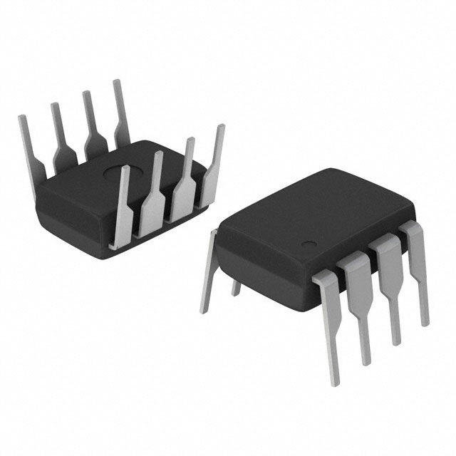
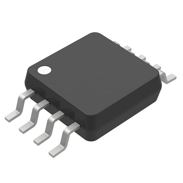
Regarding integration and mounting, the LM393DG is offered in footprint-optimized packages such as SOIC-8, PDIP-8, and Micro8™. These packages balance PCB density requirements with ease of automated assembly, facilitating quick prototyping and high-throughput production. This flexibility supports a range of deployment—from compact wearable devices, where PCB area is constrained, to mass-produced automotive dashboards requiring robustness and cost efficiency. Placement and routing are simplified by the comparator’s straightforward pinout, and external pull-up resistors can be tuned for the desired output logic swing and speed.
A unique practical strength of the LM393DG arises in mixed-voltage systems. When integrating analog front ends with modern microcontrollers, mismatched I/O levels often complicate signal translation. The open-collector outputs permit direct connection to MCU inputs—regardless of whether those inputs use 3.3 V or 5 V logic—by simply choosing an appropriate pull-up resistor tied to the target logic rail. This property not only cuts BOM components but also reduces debugging iterations and enhances system reliability.
A subtle advantage of the LM393DG, often underappreciated, is its immunity to supply sequencing and power-up transients owing to its ground-sensing input and robust input structure. In systems where supply rails ramp in unpredictable order or feature brown-out behavior, the comparator reliably asserts output states without oscillation or latch-up—even before the main controller has booted. This makes the device a go-to choice in power-good indicators, supervisor circuits, and watchdog implementations.
Overall, the LM393DG encapsulates a balance of electrical performance, application versatility, and integration convenience. When evaluated as a platform solution within analog signal chains, it supports cost-effective and resilient comparison functions across consumer appliances, industrial instrumentation, and automotive subsystems. Its enduring industry adoption stems not only from electro-mechanical reliability but also from subtle engineering details that address real-world mixed-signal challenges.
Key Features and Performance Characteristics of LM393DG
The LM393DG comparator stands out through its integration of versatile electrical characteristics, supporting a broad range of analog and mixed-signal circuit topologies. Its supply voltage adaptability allows operation from as low as 2.0 V up to 36 V in single-supply configurations, or ±1.0 V to ±18 V with dual supplies. This flexibility facilitates direct deployment across systems ranging from battery-operated low-power instruments to industrial control modules. In practice, such range minimizes design constraints when aligning with varied power rails or existing analog infrastructure.
At the core of its architecture is a low supply current draw, maintained at 0.4 mA regardless of voltage. This property enables efficient continuous monitoring tasks, such as threshold sensing or signal digitization, without imposing significant thermal or battery drain. In high node-count systems, such as multiplexed sensor arrays, reduced quiescent current becomes an enabling factor for scalable deployments without aggregate power issues.
Precision is underscored by its input parameters: input offset voltage remains tightly controlled at 2.0 mV (typical), limiting deviation in voltage comparison even at low signal amplitudes. Such performance is valuable in measurement or fault-detection circuits, where multi-millivolt fidelity between input references is needed to avoid false signaling. The comparator’s low input bias and offset currents—25 nA and 5 nA respectively—along with a ground-reaching common-mode input range, support interfacing with high-impedance elements, like resistive sensors, photodiodes, or remote condition transducers. In setups employing long wiring or high output impedances, this combination curtails erroneous input loading and drift, ensuring data integrity.
The LM393DG output employs an open-collector design, providing direct compatibility with prevalent logic standards including TTL, CMOS, and ECL. Designers can exploit this characteristic to implement wire-OR logic, level shifting, or interconnect multiple units for expanded digital processing without reciprocal loading. Additionally, saturation voltage at the output remains low enough to maintain crisp transition edges, critical in clocked measurement or timing capture subsystems.
Robustness is embedded via input ESD clamping, which materially improves survivability under transient voltage conditions encountered in industrial panels or automotive modules. This attribute simplifies compliance with EMC and reliability guidelines, reducing the footprint and cost of external protection circuitry. The device’s extended capability is reflected in the NCV2903 automotive-grade variant, which covers process and qualification requirements for high-demand transportation applications. In powertrain monitoring or safety signaling designs, adherence to such standards aligns with long-term field operation and regulatory mandates.
Distinctively, the LM393DG sustains high differential input tolerance while preserving stability across voltage and temperature extremes. System integrators routinely exploit this trait in adaptive thresholding applications, such as battery diagnostics or dynamic reference control, where input variances must translate cleanly into fast, unambiguous switching behavior. Close analysis of field implementations reveals that the device’s dual-channel configuration often facilitates compact fault monitoring, relay actuation, and PWM signal demodulation in tightly constrained layouts.
In synthesis, the LM393DG’s attribute stack—low power profile, precise input metrics, broad logic interface, and ruggedized inputs—enables exceptional integration into mixed-signal designs requiring consistent performance amid variable supplies and environmental stress. Targeted use of its strengths can yield circuits that balance efficiency, accuracy, and resilience even when exposed to operational noise or process variation.
Electrical Ratings and Operating Conditions of LM393DG
Electrical ratings of the LM393DG are essential parameters shaping the operational envelope and long-term stability of comparator-based designs. Interpreting the maximum output current rating—20 mA, unaffected by supply voltage—requires precise integration into system layouts. Although this current rating enables driving logic loads directly, circuit designers must exercise caution against output pin shorts to VCC, as the open-collector topology is prone to rapid thermal escalation, causing catastrophic device failure. Mitigation is often achieved through external pull-up resistors correctly sized for both logic high-level timing and current constraints, balancing propagation delay and power dissipation.
Thermal considerations broaden when examining the LM393DG family’s temperature specifications. Device variants serve distinct application profiles: LM393 supports commercial environments (0°C to +70°C), LM293 enables operation in moderate industrial contexts, and LM2903 as well as its V and NCV derivatives satisfy robust automotive and outdoor requirements up to +125°C. Selection hinges on deployment scenario—precision sensor interfacing within monitored enclosures favors LM393, while vibration-prone or exposed control units benefit from NCV2903. Throughout, reliable comparator behavior mandates derating component and PCB layout for ambient extremes, as comparator offset voltage and response time exhibit temperature dependence.
Input voltage limits, explicitly capped at 0.3 V below ground/minus supply and an upper common mode bound of VCC–1.5 V, dictate analog front-end architecture. Failure to enforce these restrictions invites nonsymmetrical output transitions or latch-up. In precision analog measurement, input signal conditioning circuitry such as voltage dividers or op amp buffers assure consistent operation within bounds, thereby eliminating spurious state changes under transient or noisy input conditions. Optimizing for signal integrity at the interface enhances overall system predictability.
The LM393DG’s response behavior under dynamic stimulus—defined by input step magnitude and overdrive—is a critical lever for timing-sensitive logic. A standard response time arises from a 100 mV input step plus 5 mV overdrive, but aggressive overdrive (higher differential inputs) reliably accelerates the switching edge. Tactical deployment in high-frequency signal discrimination or pulse-width modulation circuits benefits from deliberate overdrive amplification; the tradeoff is balanced against input noise immunity, demanding judicious design of signal thresholds and hysteresis, sometimes through positive feedback or Schmitt trigger augmentation.
Extensive empirical deployment reveals comparator resilience when supply decoupling is optimized and layout minimizes parasitic capacitance at input nodes. Troubleshooting often exposes marginal input exceedances resulting in intermittent mismatches or oscillations. Rectifying such issues requires not only adherence to datasheet boundaries but also an appreciation of real-world voltage excursions, laying groundwork for robust comparator selection and placement.
Overall, prudent selection and meticulous system integration of the LM393DG family—commanded by electrical and thermal boundary respect, input compliance, and strategic timing enhancement—yield reliable, application-tailored circuit solutions. Deep coupling between device parameters and use-case scenario elevates circuit immunity and performance, establishing a predictable design process and reducing failure rates.
Packaging and Mechanical Information for LM393DG
The LM393DG comparator series demonstrates well-considered packaging versatility, enabling designers to meet stringent board-level and assembly constraints. Offered in SOIC-8 (D suffix), PDIP-8 (N suffix), and Micro8™ (DM suffix) configurations, the series adapts efficiently across a spectrum of layout topologies typical in analog front-ends, mixed-signal designs, and high-density digital subsystems. Each outline provides calibrated lead pitch and standoff tolerances, ensuring compatibility both with hand-solder and automated reflow processes. The SOIC-8 balances compactness with soldering robustness, supporting SMT flows without excessive warping or co-planarity challenges, while the PDIP-8 format supports development, validation, and legacy socketed applications requiring mechanical endurance.
All available versions comply with contemporary Pb-Free initiatives, aligning to RoHS regulatory demands and minimizing process-based contamination risks—vital in eco-sensitive or medical equipment supply chains. Precision package drawing standards per ANSI Y14.5M underpin consistent mechanical referencing, mitigating dimensional ambiguity during system-level DFM reviews. The accessible footprint recommendations—frequently referenced in layout design tools—streamline padstack definition, promote uniform wetting, and optimize thermal conduction during soldering, thus reducing the likelihood of open circuits or cold joints in mass production.
The mechanical dimensionality of the LM393DG series enables seamless integration into space-constrained, multilayer PCBs where route congestion and thermal management present frequent hurdles. The Micro8™ package, with minimized Z-height and lateral dimensions, is especially effective in portable instrumentation, wearables, and point-of-load monitoring circuits. Real-world implementation often finds the LM393DG mounted adjacent to analog sensors or reference sources, leveraging the small outline for optimized node proximity and signal fidelity. Experience has shown that maintaining precise pad geometry, as prescribed in the manufacturer’s documentation, minimizes delamination and failure rates under cyclic thermal or vibrational stresses—a non-trivial concern in automotive or industrial deployments.
Unique among low-voltage comparators, the LM393DG’s availability in multiple packages with well-documented mechanical profiles accelerates design reuse across platforms and simplifies parts management in high-mix manufacturing environments. This multi-format support, when coupled with high-quality reference collateral, empowers engineering teams to optimize both electrical performance and long-term assembly yield—a pragmatic advantage particularly in cost-sensitive or safety-critical electronic assemblies.
Application Information and Design Guidelines for LM393DG
Application of LM393DG comparators is driven by their high open-loop gain and broad bandwidth, characteristics that support deployment in precision voltage comparison circuits where responsiveness and accuracy are mandatory. These devices excel in classic roles such as zero-crossing detectors, both in single and dual supply environments, highlighting their adaptability. In this context, the comparator's rail-to-rail performance and consistent response reduce the error margin in AC signal processing and waveform analysis.
The inherent architecture also allows the LM393DG to provide clean, fast edge transitions, making it ideal for free-running square-wave oscillators. Carefully selected external resistors and capacitors enable control of oscillation frequency and duty cycle. When used for time delay generation, the device leverages its fast propagation delay and predictable input-output characteristics, thus guaranteeing reliable circuit timing under varying load or temperature conditions. Integration of hysteresis through positive feedback is vital when stability is critical; it enhances noise immunity and prevents chattering at threshold crossings—a frequent requirement in environments with significant electrical noise.
Oscillation at the output during voltage transitions remains an important consideration. Coupling via parasitic capacitance from output to input poses a genuine risk of instability, especially in densely populated PCB layouts. Empirically, a combination of input resistors no greater than 10 kΩ and tightly controlled positive feedback below 10 mV effectively curbs spurious switching. Such interventions are most effective when paralleled with trace optimization and meticulous PCB layout, minimizing cross-talk and routing-related capacitive effects.
Best practices further dictate secure grounding for all unused input pins. This precaution not only suppresses latent susceptibility to stray fields and EMI but also forestalls unpredictable output states. Direct experience shows this measure significantly reduces troubleshooting effort post-assembly, particularly in mixed-signal environments where input impedance mismatches can otherwise propagate systemic errors.
A notable advantage of the LM393DG family lies in the robust tolerance of differential input voltages that exceed supply rails, provided negative excursions are kept within a -0.3 V envelope. This resilience supports flexible front-end interfacing to sensor arrays or other out-of-range voltage sources, simplifying protection circuit requirements while extending safe operating conditions. Such electrical durability translates into considerable latitude during iterative prototyping and system rework, capitalizing on the comparator's stability rather than constraining board design to theoretical margins.
Ultimately, leveraging the LM393DG's unique combination of electrical properties, judicious circuit topology, and practical design safeguards enables optimal implementation in both canonical and advanced comparator roles. By systematically addressing noise sources, input/output stability, and input integrity, the design process can exploit the full potential of the device in complex analog front ends and digitally interfaced voltage monitoring systems.
Potential Equivalent/Replacement Models for LM393DG
Evaluating alternatives to the LM393DG dual comparator centers on maintaining circuit integrity while enhancing reliability and adaptability. Several ON Semiconductor models—LM293, LM2903, LM2903V, and NCV2903—offer compatibility at both the architectural and pinout levels, streamlining substitution in both legacy and new designs.
At the electrical specification tier, the LM293 mirrors the core operating parameters of the LM393DG, including input offset voltage and propagation delay, while extending the temperature range. This feature supports deployment in industrial environments where thermal variations exceed commercial thresholds. Transitioning to the LM2903 family, both LM2903 and LM2903V maintain equivalent input threshold and open-collector output profiles. The extended ambient temperature tolerances of up to 105°C for LM2903 and 125°C for LM2903V introduce resilience in power electronics and motor control systems, often exposed to high dissipation and minimal cooling. Consistency in supply voltage and input voltage range ensures these comparators integrate seamlessly into existing analog sections without necessitating redesign.
Application-specific demands drive unique selection criteria. For domains demanding stringent reliability certification—automotive, transport, or mission-critical embedded nodes—the NCV2903 incorporates AEC-Q100 qualification. This component guarantees performance under rigorous stress testing for temperature cycling, humidity, and mechanical shock. Deploying the NCV2903 in automotive ECUs or sensor controls offers predictable endurance across a vehicle’s lifetime, minimizing field failures. Practical substitution often involves verification of footprint compatibility and minor recalibration of external pull-up values to match open-collector output dynamics, a process expedited by datasheet alignment within this family.
The layered approach to replacement emphasizes not only electrical congruence but also logistical considerations. Supply chain optimization is enabled through the interchangeability of these models, reducing dependency on single-source inventory and allowing procurement teams to respond dynamically to market fluctuations. Reliability is enhanced by leveraging multi-vendor sourcing, especially when addressing global manufacturing constraints or regulatory requirements in safety-critical contexts.
In complex systems, the practice of qualifying alternative comparators such as LM2903V or NCV2903 has demonstrated reduced downtime associated with thermal drift and increased tolerance for voltage transients. Integration with mixed-signal sensor interfaces or power monitoring circuits has revealed less susceptibility to input bias shifts over extended operational cycles, contributing to overall system stability. Subtle differentiation in packaging options—for instance, SOIC and TSSOP—enables custom layout adjustments, supporting compact designs in dense PCBs without sacrificing electrical performance.
A nuanced selection process, informed by both datasheet-level equivalence and field performance characteristics, maximizes the functional and operational landscape for analog comparators. Carefully matching extended temperature capability, automotive reliability, and supply logistics to specific application profiles delivers enduring circuit performance, operational flexibility, and risk mitigation in diverse engineering contexts.
Conclusion
The LM393DG dual comparator series demonstrates a robust architectural foundation, engineered for precise voltage threshold detection within constrained power budgets. Core to its operation is an input offset voltage typically limited to low millivolt levels, which sharply reduces false triggering in sensitive measurement systems. The part’s rail-to-rail input capability extends applicability across diverse supply scenarios, simplifying integration within mixed-signal and battery-powered platforms. Noise immunity, stemming from differential input topology and consistent common-mode rejection, is vital for stable performance in electrically noisy environments.
Industrial designers frequently leverage LM393DG’s open-drain output structure for flexible logic interfacing, whether sinking current for microcontroller GPIO signaling or driving relay controls. The output can be directly coupled to TTL, CMOS, or custom logic, bypassing translation complexities and streamlining system design. In automotive modules, reliability is enhanced by the device’s ESD protection and tolerance for wide temperature variations, aligning with the stringent standards for powertrain and safety electronics.
Package variations—including SOIC, TSSOP, and surface-mount options—support miniaturization objectives and high-density PCB layouts crucial for modern consumer devices and IoT nodes. During prototyping, its predictable propagation delay and minimal quiescent current ensure that timing-critical functions, like fault notification and voltage window detection, operate without excessive latency or risk of drift over time. Utilizing LM393DG within redundancy architectures or as part of multi-level trip-point detection chains mitigates single-point failures and supports graceful shutdown or protection policies in mission-critical applications.
Compared to alternative comparators, the LM393DG balances cost-effectiveness with advanced electrical characteristics, fostering long-term sourcing stability. When future-proofing designs, the family’s compatibility with drop-in equivalents and pin-to-pin alternatives provides flexibility for supply chain continuity and design reuse. In high-voltage interfaces or transient-prone environments, designers combine device-level features with external filtering to further suppress erratic threshold crossings, leveraging the comparator’s stable input structure.
Strategic deployment of LM393DG in hierarchical system architectures—such as primary-voltage supervisors, multi-zone fault detectors, or adaptive sensor bridges—catalyzes overall reliability and robust response. Its intrinsic versatility emerges not only from datasheet metrics but from a pattern of successful field implementations across sectors where performance, ease of design, and longevity intersect.