


 >
>


Product overview: TC7109CLW dual-slope ADC by Microchip Technology
The TC7109CLW exemplifies a class of analog-to-digital converters built on a dual-slope integration principle, optimized for applications requiring high precision and resilience to electrical noise. The device’s differential input topology enables effective rejection of common-mode noise, a frequent challenge in electrically noisy industrial environments or when interfacing with low-level transducers like bridge sensors. This attribute is accentuated by the architecture’s inherent immunity to fluctuations in reference voltage and clock frequency, maintaining accuracy over extended integration times.
Engineers benefit from the device’s single-channel, differential analog interface, which allows seamless integration with high-impedance sources or sensors where signal integrity is paramount. The TC7109CLW outputs a true 12-bit digital word following its conversion cycle, surpassing many successive approximation ADCs in noise robustness and resolution under real-world conditions. The converter’s timing and conversion logic are designed for auto-ranging scenarios, aligning well with data acquisition systems performing multi-range measurements or where input amplitudes vary widely.
From the system architecture perspective, dual-slope ADCs like the TC7109CLW demand careful attention to reference capacitor and resistor selection, as their performance directly influences integration linearity and accuracy. In practice, stability and low dielectric absorption in the integrating capacitor significantly reduce measurement drift, while precision resistors tighten endpoint linearity. Resilient printed circuit board layout further mitigates external noise coupling by segregating analog and digital planes, observing meticulous grounding protocols, and shielding sensitive traces.
The ±5V supply range and low power operation broaden the deployment spectrum, accommodating remote or battery-powered installations where thermal management or supply constraints dictate component choice. Coupled with a 44-pin PLCC footprint, system designers achieve both replacement flexibility and a cost-effective path for board-level upgrades or maintenance in legacy industrial equipment.
A nuanced advantage surfaces in calibration and field adjustment: the dual-slope method’s reliance on time rather than voltage comparison eliminates the drift and offset concerns common in other ADC types. This translates to stable, predictable measurement baselines across temperature and voltage variations—an essential trait for remote instrumentation, process control, or safety-critical monitoring, where recalibration intervals are lengthy and access is limited.
In advanced deployment, the TC7109CLW’s digital interface supports integration into microcontroller- or FPGA-based systems, simplifying serial communication tasks and supporting distributed sensor arrays. Here, the converter’s robust rejection of power supply and switching noise proves advantageous, maintaining high-fidelity signal reconstruction in electrically complex environments. By leveraging the dual-slope ADC’s unique properties, practitioners can architect measurement systems that deliver both high accuracy and reliable operation, even in deployments characterized by challenging noise profiles or long signal runs.
Key features and advantages of TC7109CLW
The TC7109CLW integrates several nuanced design elements that collectively optimize precision measurement tasks, particularly in systems demanding consistent low-noise performance and reliable signal fidelity. Its 12-bit resolution, augmented by an additional sign bit, establishes a measurement baseline capable of resolving subtle signal variations. This granularity is essential in applications such as high-precision weigh scales and industrial monitoring, where signal differentiation directly influences system accuracy.
At the core of the TC7109CLW lies a dual-slope ADC architecture. This topology is characterized by exceptional linearity and superior noise immunity, evident from its typical noise figure of only 15μVp-p. Such low noise levels enable effective acquisition of microvolt-level signals, facilitating seamless integration with bridge sensors (load cells, strain gauges) without the need for complex filtering or supplementary amplification. True differential signal and reference inputs further enhance compatibility with these sensor types, allowing direct interfacing that preserves signal integrity and minimizes error sources associated with ground loops or common-mode voltage fluctuations.
Signal handling capabilities are augmented by an impressively low input bias current (1pA typical), which is crucial when measuring outputs from high-impedance sources. This feature reduces the risk of signal attenuation, ensuring that instrumentation amplifiers and sensor networks deliver genuine readings without distortion. In practical deployments, maintaining signal accuracy over varying ambient conditions is paramount. The TC7109CLW achieves this through stringent control of drift (<1μV/°C) and non-linearity (±0.2 count typical), which collectively stabilize sensor outputs and prevent systematic errors during extended operation. This stability is particularly beneficial in industrial automation and laboratory instrumentation, where temperature fluctuations are common.
Auto-zero functionality embedded within the device streamlines calibration workflows, obviating manual zero adjustment and ensuring baseline precision. This attribute translates to measurable reductions in downtime during setup and maintenance cycles. Complementing auto-zero, advanced overload recovery features—including over-range indication and zero integrator phase—reinforce the system’s robustness by preventing data corruption and cross-channel interference in multiplexed sensor arrays. These mechanisms underpin reliable operation in multi-node environments, such as distributed sensor networks and modular test benches.
Digital communication is facilitated through byte-organized, TTL-compatible tri-state outputs, supporting both parallel bus interfaces and UART handshake mode. This dual-mode flexibility simplifies PCB layout and system integration, allowing seamless cross-compatibility between legacy and modern data acquisition platforms. The interface versatility accelerates prototyping and expedites deployment across a diverse spectrum of engineering applications, ranging from laboratory analytics to embedded field systems.
Conformance to RoHS3 and the absence of REACH restrictions are subtle yet significant design choices. They preserve long-term supply chain viability and reduce regulatory compliance overhead, positioning the TC7109CLW as an attractive solution in environmentally sensitive projects and regulated markets. The confluence of these attributes demonstrates thoughtful engineering intent, favoring balanced performance and resilient operation across multi-domain implementation scenarios.
Layering these features reveals a device crafted to minimize error sources and maximize measurement reliability. Deeper experience with the TC7109CLW underscores its utility in system-level designs requiring scalable accuracy, rapid signal recovery, and robust environmental endurance—characteristics that position it as an efficient and versatile node within high-precision instrumentation ecosystems. An implicit insight is that its combination of hardware-driven stability and flexible connectivity anticipates emerging demands for precision and integration, making it a strategically sound choice in both legacy upgrades and forward-looking architectures.
Architecture and operational principles of TC7109CLW
The TC7109CLW leverages a dual-slope integrating ADC at its core, establishing high precision through a combination of architectural features and rigorous operational sequencing. Each measurement cycle is partitioned into four clock-controlled phases, optimizing both signal fidelity and conversion accuracy.
During the auto-zero phase, the design systematically references all analog components to the system analog common. Capacitive elements are actively charged to neutralize inherent offset voltages, employing a dynamic compensation mechanism that preserves baseline integrity across varying operating environments. This procedure sharply reduces drift and low-frequency noise, which often compromise accuracy in long-term deployments. Practically, implementing a periodic auto-zero cycle is essential for applications where ambient temperature or supply fluctuations are expected; it preempts and suppresses cumulative error sources that can affect subsequent signal processing stages.
Signal integration forms the second phase, with the integrator and analog buffer directly interfaced to the differential input. The incoming signal is integrated over a fixed interval, ensuring that both amplitude and polarity are faithfully captured. Measurement polarity assignment is postponed until after integration, enabling the converter to operate symmetrically for both positive and negative inputs—a critical feature when interfacing with sensor arrays or bidirectional measurement systems. This design choice streamlines input handling, facilitating robust multiplexing strategies and error mitigation in thermal and electrical sensing scenarios.
In the reference de-integrate phase, the integrator receives the reference voltage in opposing polarity and begins the process of returning to equilibrium. The time required for this reversal is directly proportional to the magnitude of the original input, forming the quantitative foundation for the digital output. By separating the integration and de-integration intervals and capturing precise timing, the TC7109CLW effectively isolates the measurement from supply and reference fluctuations. This timing-based conversion methodology also eliminates many classical nonlinearity concerns found in successive approximation or flash ADC designs when exposed to variable analog domains.
Zero integrator phase is invoked specifically to address over-range conditions and residual charge artifacts. The architecture discharges the integrator, eradicating hysteresis and preventing signal cross-talk, which can otherwise propagate errors across channels in high-density or multiplexed systems. This phase is particularly valuable in distributed thermocouple arrays or sensor networks, where rapid channel switching may leave the integrator exposed to charge accumulation. Ensuring a clean reset between cycles is an integral tactic for achieving high repeatability in precision measurement deployments.
Supporting true differential input and reference voltages, the TC7109CLW maintains a robust common-mode range. It achieves optimal performance when analog common is close to digital ground, which simplifies system layout and minimizes susceptibility to ground loop artifacts. Designed for ±5V supply operation, the device attains a typical common mode rejection ratio of 86dB. This high CMRR is crucial for operating in environments with substantial electromagnetic interference or fluctuating ground references. Integrating these features into practical circuit layouts yields consistent results, particularly in industrial and medical instrumentation where noise immunity is paramount.
Auto-zeroing is embedded throughout each conversion cycle, enforcing real-time recalibration and minimizing offset errors. Continuous offset suppression and frequent internal referencing result in superior long-term stability, even as environmental factors shift. This architectural philosophy of recurrent baseline correction directly enhances measurement reliability and ensures consistent output across diverse operation scenarios. Experience shows that utilizing the auto-zero function, coupled with careful grounding and shielding practices, dramatically reduces field calibration requirements and maintenance overhead in deployed systems.
These layered operational principles coalesce into an architecture that delivers not only high accuracy but also exceptional robustness. Combining dual-slope integration, systematic auto-zeroing, differential measurement, and precise phase control, the TC7109CLW sets a benchmark for ADC design in applications demanding precision and stability across varying conditions. Implicit in its design is the idea that a properly sequenced and compensated ADC core can redefine the bounds of achievable signal integrity, especially in complex or adverse environments.
Electrical specifications and performance characteristics of TC7109CLW
The TC7109CLW integrates a high-resolution analog-to-digital conversion core, yielding a true 12-bit plus sign output that supports precise bipolar measurements across a symmetrical ±4V input range. Its architecture utilizes fully differential analog inputs with a wide common-mode accommodation, accepting voltages within 1.5V of either supply rail. This capability, coupled with a typical input bias current held to just 1pA, renders the device optimally suited for interfacing with high impedance sources—such as precision sensor front-ends or passive divider networks—without bias-induced measurement degradation.
Driven by an external oscillator, the conversion process operates reliably with standard 3.58MHz crystals, achieving a complete measurement cycle every 8192 clock periods. The predictable timing framework enables straightforward synchronization in multi-channel or time-critical instrumentation designs. In practice, this structure supports deterministic sampling intervals, vital for applications like weigh scales, bridge transducer signal acquisition, or low-speed data loggers where timing accuracy underpins system-level repeatability.
Signal integrity is preserved by a notably low typical peak-to-peak noise of just 15μV across the conversion range. This performance ensures that low-level analog variations are resolved with minimal quantization error and backend signal processing burden. The input stage demonstrates input-referred drift below 1μV/°C, delivering stable results under variable environmental temperatures—key for long-term deployments in instrumentation or process automation. Additionally, non-linearity remains tightly bounded, with full-scale errors limited to ±1 count, simplifying downstream calibration and enabling seamless integration into measurement subsystems where linear transfer characteristics are assumed.
The overload recovery mechanism is anchored by a zero integrator phase, actively discharging residual charge from the integrating capacitor. This rapid recovery eliminates cumulative error propagation that would otherwise arise when transient high-input events or over-range signals occur. In field deployments, this design element maintains data integrity in environments subject to unpredictable input excursions, such as in battery monitoring circuits or industrial sensor interfaces.
Digital interfacing is enhanced by robust output drive capabilities, especially pronounced in the TC7109A derivatives, where improved high-state source current ensures reliable communication with standard microcontrollers, FPGAs, or legacy TTL logic. Data outputs are organized by byte with full tri-state support, accommodating both direct parallel data acquisition and handshake-driven UART communications. This flexibility allows seamless integration with diverse system architectures, from compact embedded controllers to modular data logging hardware.
Typical quiescent supply currents, ranging from 700μA to 1500μA per supply rail, reflect a careful balance between conversion speed and energy efficiency. The device is therefore apt for both line-powered and battery-sensitive designs, supporting deployment across varied industrial, laboratory, or portable equipment scenarios.
A nuanced understanding of these parameters reveals the TC7109CLW as a refined solution where repeatable accuracy, robust interfacing, and resilience to adverse conditions are paramount. The interaction between low bias current and differential input versatility, coupled with deterministic timing and strong output characteristics, positions this converter as a cornerstone for modular data acquisition modules and precision sensor interfaces. Experience shows that leveraging well-chosen external components—such as low-noise reference sources and low-leakage input protection networks—further amplifies performance, especially in applications demanding traceable metrological standards or where margins for drift and noise are particularly constrained.
Pin configuration and functional description of TC7109CLW
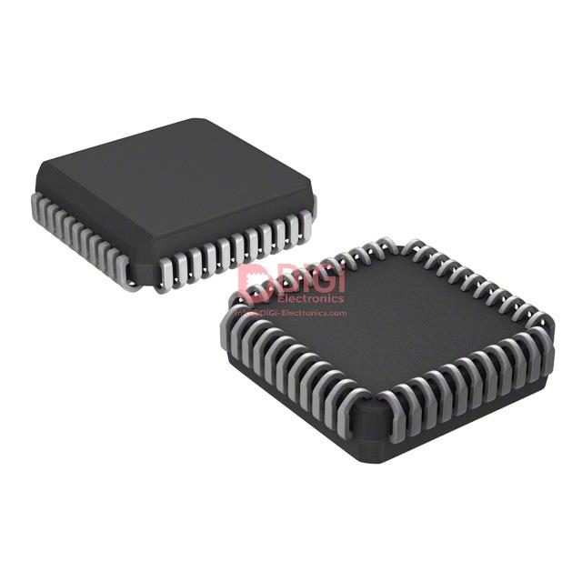
The TC7109CLW’s 44-pin PLCC package optimizes for high-density, surface-mounted assembly in complex instrumentation systems. Strategic pin allocation simplifies modular circuit design, allowing streamlined signal routing and robust platform expansion. Power supply connections—V+ and V-—are distinctly segregated, with both analog and digital ground returns, minimizing noise coupling and establishing a strong foundation for mixed-signal operation. This separation is critical in precision environments, reducing digital switching artifacts from propagating into sensitive analog sections.
The differential input architecture, featuring IN HI and IN LO, directly accepts signals from low-level sensor sources. The COMMON pin serves as an analog reference, facilitating offset compensation and efficient grounding strategies, especially when integrating multiple transducers or remote sensing nodes. Reference input/output (REF IN+, REF IN-, REF CAP+, REF CAP-, REF OUT) interfaces support tightly controlled external voltage references, essential for calibration routines and drift minimization. In practice, leveraging high-stability reference sources through these pins yields quantization accuracy exceeding the theoretical limits of simple ratiometric designs, enabling system integrators to achieve repeatable measurements across thermal and supply variations.
Digital output lines include twelve tri-state data bits, polarity, and over-range indicators. This structure enables straightforward parallel bus integration and supports multi-device environments; polarity signals track input sign changes, while over-range outputs flag excursions beyond input thresholds. These indicators are vital in real-time process control, allowing firmware handlers to respond immediately to anomalous sensor behavior or calibration needs. Tri-state operation further improves bus compatibility, ensuring seamless multiplexing and reducing contention when scaling I/O capacity.
Interface control pins—MODE, CE/LOAD, HBEN, LBEN, RUN/HOLD, SEND, and oscillator sources—provide operational flexibility. Engineers can select between direct data output and handshake modes tailored for UART or synchronous serial transfer, adapting the device for either continuous acquisition or event-driven communication. Mode control allows integration with legacy and modern systems, and additional enable lines (HBEN/LBEN) partition high and low byte transfers for optimized data pipeline management. Practical deployment reveals these pins facilitate efficient diagnostics and system testing, accelerating time-to-validation in custom hardware environments.
Auxiliary functions round out the device’s configurability. The onboard buffer amplifier, auto-zero, integrator, and test pins offer granular control over signal integrity and system debugging. Oscillator input/output pins provide adaptable clock sources for both internal timing and external synchronization; implementing custom frequency controls through these pins enables tailored throughput and power consumption regimes. In field applications, engineers frequently exploit test and auto-zero features to verify signal path linearity and preempt drift-related errors, embedding automated routines that ensure long-term platform reliability.
A layered design approach, beginning with foundational power and signal integrity, progressing to data transfer and communication strategies, and culminating in system-level customization, allows the TC7109CLW to serve in environments ranging from laboratory instrumentation to industrial process control. Integrating reference and auxiliary functions with precise signal routing techniques not only enhances measurement fidelity but establishes a platform for scalable, high-reliability architectures. A critical insight: intelligently leveraging modular pin assignments and auxiliary controls unlocks deeper integration possibilities, supporting rapid adaptation from prototype to final deployment without compromising performance or maintainability.
Package, environmental, and compliance information for TC7109CLW
TC7109CLW, encapsulated in a 44-lead PLCC format measuring 16.59 x 16.59 mm, exemplifies packaging tailored for automated surface mount processes, enabling efficient assembly and optimal board real estate usage. The PLCC form factor, with its standardized footprint, reduces layout complexity in high-density circuitry and permits reliable solder joint formation, mitigating risks associated with thermal cycling and mechanical stress. Its geometry also supports straightforward visual inspection and X-ray analysis, enhancing manufacturability and quality assurance in volume production.
The device’s environmental reliability is anchored in its commercial operating range between 0°C and +70°C, suitable for deployment in controlled indoor infrastructures such as measurement instrumentation, process controllers, and digital sensor interfaces. The Moisture Sensitivity Level (MSL 3, 168 hours) enables flexible logistics and scheduling, provided established dry bake protocols are observed prior to reflow operations. Failure to maintain these parameters can irreversibly impact package integrity, leading to microcracking or diminished electrical performance. Experience confirms that rigorous adherence to drying and humidity controls at every stage maximizes yield and reduces latent reliability issues, particularly when integrating the TC7109CLW into multi-layer PCB assemblies.
The component’s regulatory posture addresses global supply chain requirements with RoHS3 conformity, evidencing the absence of restricted substances such as lead, cadmium, and hexavalent chromium. Its exemption from REACH limitations further streamlines international sourcing and cross-jurisdictional compliance audits. This regulatory robustness removes potential bottlenecks for OEM and CEM operations, directly supporting scalable deployment from proof-of-concept prototyping to mature commercial release.
From an engineering perspective, the intrinsic CMOS architecture demands comprehensive ESD risk mitigation throughout handling and assembly. Standard antistatic measures—grounded workstations, conductive packaging, and protective garments—delimit exposure to voltage gradients and minimize the probability of gate oxide rupture. Additionally, the device’s absolute maximum ratings (+6.2V for V+ and -9V for V-) define the envelope for system-level interfacing; exceeding these bounds can catalyze transient failures or cumulative degradation. In practical circuit layouts, decoupling routines and protective clamping diodes are systematically employed near supply rails and I/O pins, providing a first line of defense against switching surges and inadvertent signal coupling.
Device integration often leverages the TC7109CLW’s resilience—combining its mechanical, thermal, and compliance attributes to anchor high-precision conversion chains in instrumentation systems. A notable insight emerges from field deployment: consistently superior field reliability is observed when conservative derating and full traceability of assembly conditions are enforced, especially in projects requiring extended operational lifespans. Implementing controlled storage, scheduled moisture pre-conditioning, and rigorous system-level protection against overvoltage events forms the foundation of fault-tolerant design practice.
In sum, the TC7109CLW exemplifies a convergence of packaging efficiency, regulatory certainty, and electronic robustness, yielding a component highly suited for demanding applications and scalable production. Its operational safeguards and environmental credentials, layered with best-practice integration routines, position it as a strategic element in advanced electronic architecture.
Potential equivalent/replacement models for TC7109CLW
When evaluating alternative solutions to the TC7109CLW, the focus first shifts to package and environmental requirements. The TC7109CKW, packaged in a 44-pin PQFP, maintains functional compatibility with the TC7109CLW while offering a compact, surface-mount form factor. This facilitates board space savings in high-density layouts or automated SMD assembly processes. For legacy systems or prototyping, the TC7109CPL presents a 40-pin PDIP, ensuring straightforward handling for through-hole designs and simplifying socketed test configurations. Where environmental extremes are present—such as industrial controls, outdoor sensing modules, or rugged instrumentation—the TC7109IJL, with its CERDIP enclosure and wider temperature rating (-25°C to +85°C), preserves device integrity and accuracy across varying thermal conditions.
From an architectural standpoint, the TC7109A series introduces refinements in drive strength and over-range recovery. These enhancements manifest as improved reliability in noisy or fast-switching environments, with the strengthened output stage directly supporting lengthy PCB traces, optoisolator interfacing, or multi-drop digital data lines. In re-engineering or forward-looking designs, these advantages substantially reduce signal integrity troubleshooting and board iterations. Notably, even minor improvements in over-range behavior minimize downtime during signal excursions, increasing overall system robustness.
When resolution requirements exceed 3.5 digits or higher accuracy is needed—such as in precision weighing, instrumentation front ends, or high-resolution process control—the TC500’s 15-bit plus sign ADC core surpasses the TC7109 series, offering finer quantization and expanded dynamic range. This device situates itself effectively in applications where quantization noise and transition uncertainty limit system performance. However, higher resolution may entail trade-offs in conversion speed or code latency, emphasizing the necessity for demand-driven component selection.
Each alternative relies on a nuanced interplay between package constraints, operating environment, and electrical performance. Experienced practitioners leverage extended temperature packages for unshielded sensor arrays, migrate to enhanced-output variants in multiplexed signal chains, and adopt higher-bit solutions in analytical measurement platforms. In deployment, relying on pin-compatible replacements can drastically streamline maintenance and field upgrades, provided that power supply, reference voltage, and interface logic remain within the new device’s operating envelope.
A systematic approach—mapping circuit requirements to package, environmental tolerance, and ADC performance—enables selection of an optimal fit within the Microchip family. This perspective underscores that value is best realized not through isolated parameter evaluation, but by integrating product characteristics with real-world deployment scenarios and lifecycle considerations.
Conclusion
The TC7109CLW, a precision analog-to-digital converter from Microchip Technology, leverages a dual-slope integration architecture coupled with true differential inputs. This architectural choice directly enhances noise immunity, a necessity for applications where signal integrity is paramount. Dual-slope conversion effectively averages input noise by integrating over a longer time window, mitigating rapid disturbances and minimizing offset errors. Differential inputs further suppress common-mode noise, strengthening measurement accuracy even in electrically harsh environments.
Analog performance is defined by input impedance, stability over temperature, and linearity. The TC7109CLW achieves high input impedance, reducing signal source loading and enabling straightforward interface with a variety of analog front-ends. Temperature drift is minimized through on-chip references and precision-trimmed components, ensuring reliable readings across fluctuating thermal conditions. Linearity, vital for accurate digitization, is maintained via careful layout, internal shielding, and matched internal signal paths—attributes critical for both laboratory instrumentation and remote sensor nodes.
Digital interfacing flexibility distinguishes the TC7109CLW in multipurpose system integration. Parallel and serial interface options permit direct connection to a wide spectrum of microcontrollers and processors. This adaptability is valuable in both new designs and drop-in replacements for legacy systems, simplifying migration without board-level rework. Furthermore, fast overload recovery enables rapid return to valid output after transient excursions, an often-overlooked feature that preserves data throughput and avoids conversion stalls in the presence of signal spikes.
Electromechanical integration is addressed through the compact PLCC package, compatible with standard automated assembly processes and well-suited to dense PCB layouts. Environmental robustness, affirmed by compliance with established industry standards, supports deployment in commercial and light industrial settings where voltage, vibration, and humidity can fluctuate.
Optimization of component choice extends beyond electrical parameters. When evaluating alternatives such as higher-resolution converters or variants in the same family, it is essential to assess package geometry, input voltage range, and established communication protocols. Systems operating at lower supply voltages or necessitating even tighter error tolerances may benefit from newer pin-compatible parts, but trade-offs in cost, latency, or software support should not be underestimated.
In practice, integrating the TC7109CLW within precision weighing systems and panel meters has demonstrated consistent conversion stability even during temperature cycles and under intermittent transient events. Deployments in field dataloggers have confirmed long-term reliability, especially where local calibration is limited or impractical. These operational contexts reveal the device’s resilience and highlight the importance of carefully matched peripheral circuitry—precision references, low-impedance grounds, and shielded traces amplify the benefits of the core architecture.
Ultimately, the most effective selection process grounds itself in a full system view, aligning TC7109CLW’s capabilities with the end application’s operational boundary conditions. The device balances mature analog design with interface versatility, offering enduring value in precision measurement domains requiring both accuracy and integration flexibility.


