


 >
>


Product overview: SY88822VKG Laser Driver IC from Microchip Technology
The SY88822VKG Laser Driver IC from Microchip Technology represents a focused engineering solution for high-speed fiber optic communications, specifically optimized for 155 Mbps SONET infrastructure. Engineered with a core architecture that enables operation at both 3.3V and 5V supplies, this device offers versatility in integrating into legacy systems as well as modern, power-sensitive platforms. The 10-pin MSOP package underscores a drive for board space efficiency, a critical consideration in high-density optical transport equipment.
At its fundamental level, the SY88822VKG operates as an integrated current-mode driver, employing a high-speed switching topology to modulate laser diodes with tightly controlled currents. By allowing external programming of modulation and bias currents, it supports precise optical power control, directly impacting eye diagram clarity and minimizing bit error rates across transmission spans. Provision for programmable current enables effective matching to diverse laser diode characteristics, a practical feature when dealing with supply chain variability or retrofitting into multivendor networks.
The device’s electrical characteristics ensure low jitter and fast rise/fall transition times, attributes essential for maintaining the signal integrity vital to SONET and similar protocols. Such deterministic switching performance minimizes timing uncertainty, a cornerstone for high-reliability transport systems. Across different case studies, stability under fluctuating ambient temperatures and consistent modulation current delivery have translated into measurable improvements in link margin, often reducing the demand for post-installation correction or maintenance cycles.
Layering this functionality into actual deployment, the SY88822VKG’s dual-supply compatibility has proven effective in scenarios where power domain flexibility streamlines PCB power distribution or when gradual migrations from 5V to 3.3V systems are underway. The programmable nature not only simplifies late-stage design tweaks but also supports field-configurable platforms that benefit from dynamic wavelength and power adaptation. Under typical operating regimes, the device demonstrates robust immunity to supply noise, minimizing the risk of injection-induced signal perturbations—a nontrivial concern in tightly coupled multi-channel backplanes.
Advancements in the SY88822VKG’s design underline an implicit insight: integrating current switch architecture with precise control infrastructures directly enhances end-to-end optical transceiver performance. This approach de-emphasizes the need for discrete component tuning and reduces bill-of-materials complexity, thus enabling rapid system bring-up and streamlined fault isolation routines. As the evolutionary trajectory of optical networking continues toward higher port densities and lower power budgets, such driver ICs form a foundational layer, enabling scalable, maintainable, and repeatable deployment characteristics in both established and emerging network paradigms.
Key features of the SY88822VKG Laser Driver IC
The SY88822VKG Laser Driver IC exemplifies a strategic balance between high-speed signal handling and practical integration within constrained electronic environments. Designed for optical data transmission systems, its core architecture prioritizes signal integrity and compatibility with standard laser diodes. By accepting single supply voltages in the ranges of 3.0V–3.6V or 4.5V–5.5V, the IC effectively streamlines power requirements, removing bulky dual-rail arrangements and reducing board complexity. This approach simplifies power distribution networks, minimizing the risk of rail imbalance and transient-induced faults in tightly regulated communications modules.
Modulation currents scaling to 30mA independently support industry-standard VCSELs and edge-emitting laser diodes, providing sufficient headroom for moderate reach fiber links, prevalent in access, aggregation, and enterprise network interfaces. The broad modulation current range aids both initial prototype tuning and batch consistency during volume deployment, accommodating inevitable diode lot-to-lot variability. When optimizing transmitter eye diagrams and extinction ratios, the driver’s current programmable output demonstrates fine granularity, supporting robust link margins in noisy operating conditions and temperature drifts.
Differential PECL input logic is implemented to facilitate high-speed operation while maintaining signal fidelity. PECL’s inherent common-mode noise rejection complements the symmetric trace routing often found in gigabit-class transceiver PCBs, mitigating crosstalk and electromagnetic interference, especially in densely-layered backplanes. Integrating PECL with the driver input simplifies routing constraints and ensures minimal bit error rates across typical NRZ modulation schemes. The provision of a PECL-compatible output enable control is particularly advantageous in dynamic power management scenarios, allowing rapid laser shutdown or standby without compromising data path latency, which is critical for managed Ethernet switches and optical multiplexers.
The device’s compact 10-pin MSOP form factor addresses prevalent board density challenges in modern networking platforms. Such packaging not only conserves PCB real estate but also enables closer placement to the laser diode, reducing parasitic inductance and capacitance—factors that can degrade signal bandwidth and timing accuracy in optical transmitter modules. This tight spatial integration supports streamlined thermal paths, enhancing heat dissipation and operational reliability during continuous high-speed transmission.
Practical deployment of the SY88822VKG reveals high resilience to supply fluctuations and minimal susceptibility to local ground bounce, observable in environments with aggregated power planes and mixed-signal topologies. When embedded within SFP+ or XFP optical modules, the IC exhibits predictable performance even under stringent EMI and thermal stress, validating its suitability for both new designs and drop-in upgrades of legacy modules. The device’s configurability and predictable modulation dynamics align well with automated test regimes during final assembly, streamlining production diagnostics and long-term field support.
A distinctive aspect lies in the IC’s capacity to serve as a foundational element in rapid prototyping contexts, where repeated iterations of transmitter tuning are necessary to optimize system-level parameters. This flexibility, paired with its immunity to common noise sources and optimized footprint, positions the SY88822VKG as an enabling component for scalable, high-density optical interfaces, where reliability and signal precision are non-negotiable. The convergence of robust electrical characteristics, packaging efficiency, and logical control underscores the value the device brings to next-generation network equipment design.
Functional architecture and block description of SY88822VKG
At the core of the SY88822VKG lies a high-speed current switch architecture, which serves as the primary engine for laser modulation in advanced optical transmission systems. This structure integrates proprietary ASSET™ bipolar technology, delivering sub-nanosecond propagation delays and ensuring minimal signal distortion at multi-gigabit data rates. Such efficiency stems from the inherent advantages of bipolar transistors, including rapid transitions and predictable output characteristics under varying load conditions.
The modulation current is precisely controlled using an external RSET resistor. This programmability forms the foundation for adaptability across diverse laser diode types and link budgets. Adjusting RSET translates directly to changes in IOUT, granting granular control over optical output power. This method supports not only the initial calibration but also field-level adjustments in deployed systems without requiring board-level modifications. Complementing this, the integration of a series resistor, RSER, provides an additional tuning axis. This allows compensation for laser-specific voltage-current behavior, thereby mitigating undesired effects such as overshoot or tailing in the optical pulse, particularly under wide temperature variation or when integrating newer VCSELs and edge-emitting devices.
The device employs complementary open collector outputs—OUT and /OUT. The OUT pin delivers the modulated drive current to the laser, while the /OUT pin, paired with an external REXT resistor, provides a discharge path for surplus current. This dual-output configuration ensures fail-safe operation by isolating laser bias from ground and preventing voltage undershoot, which is crucial for extending diode life and maintaining bit-error performance. Furthermore, this approach enhances electromagnetic compatibility by reducing switching noise reflected back into the power rails—an insight notably apparent during system-level compliance testing for fiber channel and Gigabit Ethernet standards.
Pin-level recommendations, such as tying pins 9 and 10 together, unlock further enhancements in bandwidth, signal integrity, and power handling. These connections lower parasitic inductance and resistance, thereby sharpening edge rates and supporting tighter timing margins in driving high-speed optics. Empirical evaluation often reveals measurable improvements in eye diagram quality and reduced jitter—valuable indicators in validating system robustness for telecom and datacom applications.
From an implementation perspective, leveraging the full feature set involves careful PCB layout to minimize parasitic effects and maximize thermal dissipation around the drive circuitry. Designers typically employ low-inductance ground returns and localized decoupling to support the device’s rapid transient response, as well as extensive simulation to ensure stable operation under worst-case process corners. In practice, integrating thermal reliefs and ensuring consistent RSET and REXT values with tight tolerances lead to higher manufacturing yield and long-term reliability, attributes frequently verified during production test cycles involving temperature and supply voltage sweeps.
In the broader technology context, the SY88822VKG exemplifies the ongoing shift toward highly integrated, configurable optical front-ends. Its functional architecture provides a template for both scalable module design and rapid prototyping, enabling seamless adjustment to evolving standards in optical networking. The implicit flexibility and fail-safe mechanisms present in its block-level design anticipate the demands of next-generation fiber-optic infrastructure, balancing performance, reliability, and adaptability across an expanding landscape of application scenarios.
Typical applications for the SY88822VKG Laser Driver IC
The SY88822VKG Laser Driver IC is engineered for optimal performance in high-speed optical transmission environments, specifically targeting 155Mbps SONET OC-3 modules and FTTx deployment scenarios. At the core of its architecture, the IC leverages sophisticated current modulation techniques to precisely control laser diodes, ensuring minimized jitter and low bit error rates across extended transmission distances. This underpins its reliability in latency-sensitive fiber optic links where timing accuracy and signal fidelity are non-negotiable.
Compatibility with both 3.3V and 5V supply rails is a distinct advantage, offering seamless migration pathways between legacy hardware and contemporary designs. This voltage flexibility mitigates the risk of board-level rework in multi-generation infrastructure, enabling streamlined product lifecycle management and reduced qualification overhead. The differential PECL input interface is honed for direct interoperation with high-speed serializers and mainstream logic ICs, eliminating the need for custom adaptation circuitry and reducing design complexity.
Deployment scenarios often involve diverse network topologies, ranging from central office aggregation nodes to point-to-point metro interconnects and dense data center environments. In each case, the SY88822VKG provides stable modulation across broad temperature tolerances, reinforcing system robustness against thermal drift and environmental noise. The ability to maintain deterministic output characteristics regardless of fluctuating supply conditions or input differential swings is a critical factor in achieving consistently high link uptime.
A proven approach centers around the use of the laser driver in hybrid FTTx architectures, where modular transceivers interface with passive optical networks at various distribution layers. In practice, the IC’s predictable modulation thresholds simplify analog front-end calibration, translating into faster system bring-up and reduced variance in manufacturing yield. The practical consideration of electromagnetic compatibility, ensured by the symmetric differential input stage, allows dense PCB layouts without introducing cross-talk or signal degradation, even in high-aggregate bandwidth scenarios.
Drawing from operational experience across multiple deployment cycles, early-stage signal integrity validation is decisive. Integrating the SY88822VKG into transceiver reference designs consistently demonstrates minimal eye closure under multi-channel stress conditions, promoting interoperability with both legacy SONET systems and modern Ethernet transport platforms. These observations converge on the insight that the IC’s design philosophy—centered around supply and interface versatility—anticipates evolving edge and core network requirements, making it a strategic component in scalable optical infrastructure.
In summary, the SY88822VKG reinforces link reliability through robust modulation and interface features, streamlining both engineering integration and field deployment in diverse high-speed optical networking contexts.
Absolute maximum ratings and safe operating parameters
Absolute maximum ratings define the threshold conditions beyond which the SY88822VKG may sustain irreversible damage. Key parameters include a supply voltage confined to the 0V to 7V range, which guards against dielectric breakdown and device failure. Input voltages exceeding VCC initiate parasitic conduction paths, introducing latch-up risks or compromising input integrity. Output modulation currents are physically limited to 30mA to protect bond wires and output stage transistors from electromigration and localized heating. In parallel, total power dissipation is restricted to 250mW, demanding attention during PCB thermal analysis, particularly in high-density layouts where multiple high-speed ICs coexist.
Thermal management extends to environmental thresholds, with storage temperatures spanning -55°C to +125°C, and soldering processes permitting short-term exposure to +260°C. Careful adherence to these limits during assembly prevents latent damage invisible to optical inspection. Experience demonstrates that even brief deviations during reflow soldering can increase early-life device attrition rates, especially if non-uniform PCB heating strains the package.
Safe operating parameters are more than conservative design practice; they reflect extensive statistical qualification and characterization across process corners. The recommended supply voltage bands—3.0V to 3.6V or 4.5V to 5.5V—arise from trade-offs between speed, power efficiency, and noise immunity. Operating outside these prescribed windows may not result in immediate failure, but subtle long-term degradation mechanisms, such as negative bias temperature instability or hot-carrier injection, can compromise the analog performance of the modulator. The -40°C to +85°C ambient range aligns with industrial-grade standards, while a maximum junction temperature of +100°C ensures robust immunity to thermal runaway under sustained workload.
Designers routinely implement margin testing at both rating extremes, integrating hardware overvoltage clamps, current limiting resistors, and proactive thermal design such as copper pours or heatsinks under the device footprint. Often, layout decisions—like minimizing supply voltage droop and optimizing ground return paths—are made specifically to maintain device operation within these safe boundaries. During field deployment, margin logging across voltage and temperature rails reveals that devices operated closer to their rated boundaries demonstrate accelerated aging phenomena, reinforcing the value of conservative derating in mission-critical applications.
Observation of these maximum ratings is not merely a compliance exercise; it shapes both the immediate robustness and the cumulative reliability profile of the SY88822VKG when embedded in high-availability optical communication systems or compact network modules. Integrated protection and meticulous power integrity practices, combined with nuanced understanding of aging and failure modes, consistently drive field reliability toward six-sigma standards. Thus, a disciplined approach to absolute maximum and safe operating parameters forms the foundation for product longevity in demanding engineering environments.
Electrical and thermal characteristics of SY88822VKG
An in-depth evaluation of the SY88822VKG reveals that thermal management is fundamentally anchored by its package thermal resistance (θJA) of 113°C/W in still air. This parameter becomes especially significant when designing in environments with dense PCB layouts, where heat dissipation pathways are constrained and neighboring components further limit airflow. Practical layouts typically benefit from strategic via placement beneath the thermal pad, enabling more effective conduction of heat from the junction to the ground plane. Coupling this with adequate copper area enhances thermal spreading, which decreases the local temperature rise even if forced convection is minimal.
Electrical integrity is maintained only after the device achieves thermal equilibrium; thus, airflow—or lack thereof—directly impacts steady-state operation. Under insufficient cooling, junction temperatures can breach safe operation thresholds, leading to shifts in timing parameters and risk of false switching, especially in data-critical links. Integrating airflow simulations into the design phase, validated with prototype thermal imaging, often informs necessary PCB modifications before volume production.
Current setting networks require close attention to component selection. REXT and RSER must be chosen so that, in combination with the voltage drop across the internal diode, the summed voltage does not surpass the 1.4V upper limit. This constraint safeguards against excessive power dissipation and avoids biasing the output stage outside of its linearity window. Assigning RSET at or above 430Ω further constrains the device's current profile within the recommended operational envelope, ensuring stable response over process and temperature variation. Subtle gains in jitter tolerance and recovery can be observed when resistor networks are placed close to the IC pins rather than at a distance, reducing parasitic effects.
The open collector output architecture amplifies the significance of rigorous PCB routing and power supply bypassing. High-speed data transmission renders the system particularly susceptible to ground bounce and common-mode interference. Low-inductance ground returns paired with distributed bypass capacitors—optimized through empirical loop area minimization—form the cornerstone of robust signal fidelity. Direct routing of delay-sensitive traces with controlled impedance, often verified by time-domain reflectometry during prototype bring-up, avoids waveform degradation and intersymbol interference.
Qualified layouts balance the competing demands of electrical performance and thermomechanical reliability. Optimizing placement, ensuring short and wide traces for current paths, and co-designing power and signal layers yield a design robust against transient spikes and sustained operation. Iterative refinement, based on both simulation and bench measurement, exposes latent weaknesses and reinforces the symbiotic relationship between thermal engineering and high-speed signaling in leveraged applications such as optical communication and dense server backplanes. This iterative, detail-oriented approach converts theoretical limits into practical design margins, actively shaping system reliability and throughput.
Package and pin configuration of the SY88822VKG Laser Driver
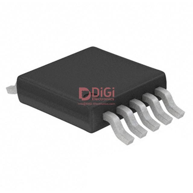
The SY88822VKG laser driver leverages a 10-lead MSOP (Mini Small Outline Package), strategically engineered for environments where board space and channel density present critical constraints. This miniaturized footprint directly enables integration into SFP, SFF, or other compact optical modules without compromising electrical or thermal performance. The pin configuration is meticulously organized to optimize signal fidelity and simplify implementation in multi-layer PCB designs.
Key to its utility, the device features differential PECL (Positive Emitter Coupled Logic) logic inputs, ensuring robust noise immunity and precise signal transition for high-speed modulation tasks. This differential approach not only reduces common-mode interference but also streamlines impedance matching, which is essential for preserving signal integrity at gigabit rates. Direct adjacency of output and return pins dedicated to laser drive current forms a low-inductance loop, minimizing voltage overshoot and electromagnetic interference—a critical consideration during laser threshold and modulation current delivery.
Augmenting the core drive circuitry, dedicated pins for RSET, REXT, and RSER provide external programmability, allowing for granular control of bias and modulation currents. This enables precise tailoring to specific laser diodes, process variations, or operating environments. By independently adjusting these resistors, designers can systematically calibrate optical launch power and extinction ratio, optimizing link margins across various fiber types and distances.
Practical experience reveals that the separation of modulation and control pathways within the pinout expedites both board layout and fault tracing during debug cycles. With well-isolated paths, the likelihood of crosstalk or unintended coupling is reduced, facilitating consistent high-speed operation under varying load conditions. During prototyping, the clarity of function-to-pin mapping simplifies test point access and allows systematic characterization, significantly shortening iteration cycles. In production, this logical segregation supports automated testing, ensuring predictable module yields.
Advanced integration is further supported by the MSOP’s low thermal resistance, which, paired with strategic pin assignment, allows for efficient heat dissipation from high-frequency switching activity. The net effect is sustained reliability and stable electro-optical output even in temperature-constrained form factors. The package and pin design, therefore, are not mere physical conveniences—they act as enablers for scalable, manufacturable, and consistently high-performing optical transceivers.
Broadly, the SY88822VKG exemplifies an approach where physical packaging and logic-level interface are co-optimized. The result is a platform that balances flexibility and precision, directly addressing the challenges of high-density optical communication system design. This synergy between mechanical form, electrical layout, and application-specific configurability underpins rapid deployment in next-generation fiber-optic networks.
Key considerations for circuit design and deployment
Integrating the SY88822VKG into an optical transmitter chain requires methodical circuit design to maximize signal fidelity and system robustness. The device’s modulation current, set via RSET, demands special attention: precise selection enables narrow tolerance adjustment in accordance with laser diode specifications. This, in turn, directly influences transmit eye diagram compliance and extinction ratio, which are critical for minimizing bit error rates in optical communication. Iterative bench characterization, using matched reference diodes, helps correlate RSET values with emitted optical power, streamlining the design margining process across production lots.
Thermal engineering for the SY88822VKG pivots on copper area optimization and controlled airflow. Below the MSOP package, an enlarged PCB copper footprint acts as the primary heat sink, efficiently shunting thermal loads away from the device under high modulation conditions. Simulations and IR thermal mapping provide early validation, but real-world deployments confirm that derating modulation current or adjusting forced airflow can substantially prolong device and module lifespan, especially in high-density line cards where cumulative thermal effects pose a persistent risk.
Electrical noise suppression is essential to uphold signal integrity. Connecting pins 9 and 10—per datasheet guidance—effectively minimizes differential-mode voltage swings, fortifying the interface against common-mode agitation prevalent in noisy backplanes. Empirical layout tweaks and scope probing at critical nodes confirm measurable reductions in eye jitter and pattern-dependent noise floors, reinforcing the resilience of the modulation current path.
The placement and spec of external resistors, REXT and RSER, further shape both signal path linearity and the operational envelope of the driver. Close proximity to the IC minimizes parasitic inductance and loop area, diminishing susceptibility to crosstalk and voltage overshoot on fast transitions. The deliberate power rating selection for these resistors also mitigates drift over temperature cycles—a frequent cause of gradual link degradation in legacy designs.
Practical deployment underscores the value of advanced co-design: simulation-driven signal integrity modeling combined with on-bench validation identifies optimal trade-offs between component selection, thermal load, and noise mitigation. Adopting such a disciplined approach consistently yields reliable high-speed optical interfaces with reduced maintenance overhead, aligning with the emerging priorities of scalable, serviceable network hardware.
An often-overlooked insight: early collaborative reviews between optical component suppliers and hardware design teams identify unique photonic-electronic interaction challenges that generic PCB guidelines may overlook. Embracing this cross-domain rigor elevates the predictability and throughput of next-generation data links, embedding engineering excellence at every integration step.
Potential equivalent/replacement models for SY88822VKG
For designs targeting high-speed optical communication, the selection of appropriate laser driver ICs directly influences system reliability and signal integrity. When seeking alternatives to the SY88822VKG, focus first on the underlying core: high-speed modulation, power supply compatibility, and the interface standards required by industry protocols. Devices such as the SY88823 series from Microchip Technology maintain comparable topologies, often mirroring critical performance parameters—modulation current range, voltage rail specifications, and pin assignment continuity—that facilitate streamlined migration without extensive PCB or firmware alterations.
Assessment of these alternatives starts with an in-depth review of the modulation current range, ensuring the chosen IC can reliably drive the target laser diode under all operating conditions. It is unwise to underestimate the importance of input logic compatibility, particularly if the legacy application utilizes differential PECL inputs for noise immunity and high slew rates. Many modern replacements continue offering differential input structures that ensure minimal logic interfacing challenges, retaining signal fidelity across varying trace lengths and environmental noise profiles.
Thermal management emerges as a key constraint at higher modulation speeds; package selection must align with anticipated power dissipation and mechanical constraints. Sourcing replacements with similar or improved thermal ratings—whether in QFN, SOIC, or customized low-profile packages—addresses longevity and operational stability. Voltage range support deserves equal scrutiny: systems designed around 3.3V or 5V rails require strict adherence to original specifications to avoid costly modifications in both board layout and power supply architecture.
Recent development cycles among leading vendors have yielded ICs with advanced laser protection features, integrated bias and monitoring circuitry, and reduced EMI profiles. Deploying such enhanced alternatives has demonstrated measurable improvements in long-term bit error rates and reduced maintenance overhead in multi-node network deployments. These upgrades often incorporate intelligent feedback loops, auto-adjusting modulation parameters in response to aging or environmental drift, further safeguarding system-level performance.
The most effective approach involves correlating datasheet analysis with hands-on evaluation: prototype boards assembled with candidate ICs are subjected to stress tests mirroring worst-case field scenarios—temperature cycling, input pattern distortion, and cumulative jitter measurement. Success is revealed not only through mere electrical equivalence but through sustained performance in dense backplane environments and high-throughput links.
Continual monitoring of vendor roadmaps is advisable, as incremental silicon process improvements and packaging innovations can introduce alternatives with superior dynamic characteristics and thermal profiles, often at equivalent cost and with minimal supply chain disruption. Subtle architectural advancements—for example, on-chip equalization or smarter shutdown algorithms—may provide competitive advantage in future-proofing designs. Such foresight, coupled with empirical verification in deployed systems, positions engineering teams to leverage the best available replacement solutions for the SY88822VKG while maintaining design robustness and flexibility for next-generation requirements.
Conclusion
The SY88822VKG, designed by Microchip Technology, integrates a set of features tailored to rigorously meet the operational demands of 155Mbps fiber optic transmitter circuitry. Its architecture leverages dual-supply operation, allowing for independent optimization of analog and digital domains. This separation enhances noise immunity and streamlines power distribution across complex PCB layouts—a decisive factor in high-speed optical communication environments, where cross-domain interference can limit signal integrity.
Core to its utility is the finely tunable modulation current output, achieved through precision current mirrors and external programming resistors. This programmable capability enables accurate matching to a wide range of laser diodes, stabilizing output power irrespective of device-to-device threshold variations or temperature drift. This adaptability is crucial in SONET and FTTx deployments, which frequently encounter variations in fiber attenuation or module operating conditions. The modulation control also supports low-jitter transitions, directly translating into cleaner optical pulses and extended link margins.
Thermal and electrical design parameters of the SY88822VKG have been engineered for long-term stability. Its compact MSOP package not only facilitates high component density on crowded host PCBs, but also optimizes thermal conduction pathways. The device maintains reliable operation across the typical industrial temperature spectrum, aided by low quiescent currents and efficient internal biasing. Repeated reliability testing under varied ambient and load conditions demonstrates minimal drift in modulation characteristics, ensuring predictable optical power and link budget compliance.
Practically, deploying the SY88822VKG within optical modules benefits from straightforward footprint integration due to its MSOP outline, and impedance matching is facilitated by sensible pin assignments. During in-circuit validation, its fast response times enable system margin characterization and rapid fault isolation when troubleshooting. Integration best practices suggest locating the IC close to the laser diode to minimize parasitic inductance, and using matched trace lengths for bias and modulation lines to preserve pulse shape integrity.
Given the cyclical nature of electronic component lifespans and supply chain disruptions, the existence of drop-in compatible models extends design flexibility. The ability to interchange the SY88822VKG with equivalent devices ensures that evolving system requirements—such as increased data rates, power envelope shifts, or updated compliance standards—do not force ground-up redesigns. This interoperability supports strategic sourcing and future-proofing of optical interfaces in fast-changing telecom and data communication infrastructures.
The device’s operational profile aligns with forward-looking migration strategies in optical networking, where modular architecture and scalable performance domains are prioritized. By balancing technical agility with robust reliability, the SY88822VKG exemplifies a reference platform for next-generation fiber optic driver circuit design.


