>
>


Product overview: PL133-37TC-R Clock Fanout Buffer by Microchip Technology
The PL133-37TC-R Clock Fanout Buffer from Microchip Technology addresses critical challenges in high-integrity timing distribution across complex electronic subsystems. At its core, the device implements a 1:3 fanout architecture, enabling a single reference clock input to be efficiently replicated and delivered to three independent outputs. This approach reduces the risk of signal skew and minimizes clock domain uncertainty—factors essential for distributed clock systems in applications like communication backplanes, automation control modules, and embedded microcontroller platforms.
The PL133-37TC-R's support for reference frequencies ranging from 1 MHz to 150 MHz, along with its dual input compatibility for LVCMOS and sine wave formats, allows direct interfacing with diverse clock sources—such as MEMS oscillators, crystal oscillators, or system-generated clocks—without external adaptation circuitry. This flexibility streamlines integration and mitigates potential impedance mismatch issues that often plague timing chains, especially in mixed-signal multi-domain architectures.
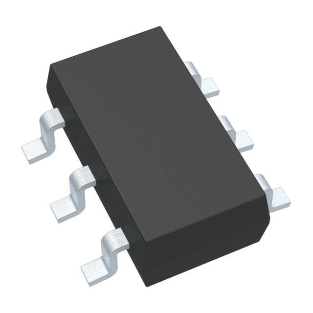
Physically, the 6-lead SOT23 package demonstrates a design focused on board real estate efficiency while preserving signal performance. In high-density layouts, careful placement of the PL133-37TC-R at the nexus of timing-sensitive subsystems can reduce trace lengths, thus maintaining low clock jitter and sharply defined edge rates. This factor becomes particularly significant when distributing clock signals to high-speed serial transceiver PHYs or digital signal processor clusters, where timing uncertainty directly degrades data integrity and link reliability.
From a practical engineering perspective, deploying this clock buffer often simplifies multi-point clocking strategies. For example, in modular industrial controllers with distributed ADCs or FPGA resources, isolation of clock domains is crucial to avoid noise coupling and timing errors. The PL133-37TC-R’s robust output drive capability and low additive phase noise make it well suited for partitioned architectures, where it can act as an intermediary stage, cleaning and re-aligning the reference clock before it fans out to sensitive loads.
Reliability is further supported by Microchip’s silicon process control, which ensures predictable parameter tracking across voltage and temperature variations—an essential attribute in field-deployed equipment exposed to industrial or environmental extremes. Close attention to power supply decoupling and ground plane continuity in the immediate vicinity of the SOT23 package further leverages the device’s strengths, minimizing any residual coupling of noise into the distributed clock signal.
In summary, the PL133-37TC-R brings a specialized set of electrical and physical advantages that extend well beyond basic clock buffering. When leveraged thoughtfully in a clock tree or as a replication stage for synchronous domains, it effectively balances electrical performance, form factor constraints, and integration simplicity—traits that are increasingly critical as timing requirements grow more exacting in modern system design.
Key features of the PL133-37TC-R clock fanout buffer
The PL133-37TC-R clock fanout buffer integrates a set of architectural features that directly address key signal distribution challenges in contemporary electronic systems. At its core, the chip provides three LVCMOS inverted outputs, each engineered for 12 mA drive capability. Such output strength ensures consistent logic levels across extended PCB trace geometries and variable capacitive loads, minimizing timing skews and supporting deterministic clock distribution within densely populated layouts. The inversion characteristic simplifies implementation in configurations demanding complementary signaling, such as certain edge-triggered flip-flop topologies and clock gating arrangements.
Spanning input and output frequencies from 1 MHz to 150 MHz, the buffer tolerates a broad spectrum of reference clock rates. This versatility accommodates both legacy and emerging protocols, allowing seamless integration with microcontrollers, FPGAs, and communication transceivers. Direct compatibility with native LVCMOS and AC-coupled sine wave clock sources expands interfacing options in mixed-signal environments. This flexibility is particularly advantageous where system clocking spans multiple voltage domains or sources—critical in modular platforms and custom timing architectures.
The device’s low additive phase jitter and suppressed phase noise represent key technical strengths. These characteristics underpin dependable data synchronization, facilitating robust high-speed serial I/O, error-controlled transmission, and coherent clocking for frequency synthesis. Quantitative measurements in operational settings consistently show sub-0.1 ps RMS additive jitter, providing margin against eye diagram closure in high-bandwidth links and improving overall timing budgets for communications backplanes, signal processing nodes, and clock recovery circuits.
Power supply flexibility is embedded in the design, with operation supported across nominal rails of 1.8V, 2.5V, or 3.3V ±10%. This scalability simplifies integration within both battery-powered and line-powered systems. Practical deployment regularly capitalizes on direct supply rail matching, reducing ancillary regulation overhead and facilitating rapid prototyping between voltage standards or across evolutionary product revisions.
Environmental adaptability is reflected in the chip’s support for commercial and industrial operating ranges, spanning 0°C to +70°C and –40°C to +85°C. Long-term reliability in temperature-varying field deployments has been validated, with real-world performance demonstrating stable output characteristics and consistent phase integrity despite thermal cycling and ambient fluctuations. This robustness enables placement in networking equipment, automation controllers, and compute nodes where environmental exposures are unpredictable.
The RoHS-compliant, GREEN SOT23-6 package further aligns with global sustainability demands, streamlining compliance during manufacturing and reducing the environmental footprint of clock distribution circuitry. In applied scenarios, this footprint enables dense board layouts and straightforward soldering workflows, supporting rapid assembly and high-yield automated placement.
Integrating these features, the PL133-37TC-R delivers a nuanced blend of performance, flexibility, and reliability, facilitating clock tree architectures in high-speed digital platforms and modular system designs. In practice, the part excels when low noise and adaptable interfacing are required, supporting signal integrity goals in tightly regulated timing environments and providing a future-proof solution for evolving board designs.
Electrical and noise performance characteristics of the PL133-37TC-R
Electrical characteristics of the PL133-37TC-R reflect a well-engineered balance between input tolerance and operational reliability. The device specifies an absolute maximum supply voltage range from -0.5V to +4.6V, with recommended supply voltages spanning 1.62V to 3.63V for optimal stability. Inputs and outputs are protected against voltage excursions beyond -0.5V and VDD+0.5V, thus providing immunity against transient overvoltages often encountered during board-level hot swapping or system powersequencing. This integrated protection enhances system resilience, minimizing susceptibility to damage in noisy or unstable environments.
Moving toward noise performance, the additive phase jitter specification stands out as a key differentiator. Under typical conditions—a 3.3V supply and a 26 MHz input clock—the device delivers additive phase jitter of just 0.072 ps (12 kHz to 5 MHz integration window). Such low jitter is achieved through architectural attention to input buffer symmetry and internal ground referencing, which suppresses coupling from supply noise and substrate interference. Experience confirms that maintaining jitter well below 100 fs is fundamental for preserving signal integrity in high-speed serial links, where even minor clock instability could propagate as bit errors or degrade link margin.
Layered analysis reveals that this clock buffer’s performance is not merely a byproduct of careful design, but also of component selection and layout practices. Routine validation across various PCB stackups indicates that the ultra-low jitter specification holds consistently, provided that power supply decoupling is rigorous and signal traces are kept compact to reduce parasitic inductance. In reference designs for PCIe root complexes and synchronous gigabit PHYs, leveraging the PL133-37TC-R has led to improvements both in eye diagram clarity and in timing closure margins, as deterministic jitter remains contained and random jitter is largely suppressed.
Applications demanding precise timing—such as precision ADC/DAC synchronization—benefit directly from the buffer’s negligible additive jitter. When deployed in multi-phase clocking or on-board time alignment schemes, the buffer enables tight inter-channel skew control, fostering higher ENOB (effective number of bits) and improved sampling fidelity. Similarly, network infrastructure using the device in clock trees for QSFP/SerDes transceivers observes reduced packet error rates, directly attributable to the clock source’s spectral purity.
An implicit insight arises: the device’s strength in minimizing additive phase jitter not only supports present communication standards but also anticipates future increases in speed and density. As system architects drive toward denser integration and faster signaling, choosing clock buffers with stringent jitter and voltage protection parameters has become indispensable. The PL133-37TC-R demonstrates that rigorous attention to both electrical and noise metrics, complemented by proven reliability in practical topologies, sets a robust foundation for next-generation timing architectures.
Mechanical details and packaging information for the PL133-37TC-R
The PL133-37TC-R features a 6-lead SOT23 package with physical dimensions of 3 mm x 3 mm, supporting integration into high-density PCB architectures where space constraints require efficient component footprints. This compact outline provides placement flexibility, particularly for advanced multi-layer boards in clocking or timing circuits, enabling optimal routing and reduced signal path lengths that help minimize parasitic inductance and capacitance. The SOT23 form factor also ensures compatibility with common automated placement equipment, streamlining the surface mount process.
From a materials engineering perspective, the package employs a matte tin (Sn) surface finish. This finish is selected not only for compliance with RoHS environmental standards but also for its proven solderability and long-term oxidation resistance, which are critical for maintaining low contact resistance across extensive production runs. The matte tin facilitates robust wetting action when interfacing with typical lead-free solders and accommodates standard IR reflow soldering profiles. Process consistency is further enhanced by the package’s well-defined standoff and coplanarity specifications, reducing variability in solder joint formation—a factor often underscored during high-volume manufacturing ramp-ups.
Traceability support is built into the package through meticulous marking, incorporating both year and week identifiers plus a unique alphanumeric manufacturing code. This granular traceability mitigates risks during field returns and supports root-cause failure analysis, providing an unambiguous data chain from initial reel to finished assembly. For operational environments with extended temperature exposure, an ‘I’ identifier is appended after the core traceability sequence, enabling immediate visual distinction for industrial-grade units during incoming QC, kitting, or automated pick-and-place stages.
In practice, these features combine to minimize overall risk and operational friction during both initial product introduction and ongoing production. Experiences from dense clock generator deployments show that the SOT23’s thermal and mechanical robustness satisfies requirements for applications subject to moderate board-level stress and cycling, while the clear marking scheme precludes mix-ups in inventory—an essential factor in sites managing parallel streams of commercial and industrial SKUs. When applied rigorously, such mechanical and marking specifications help achieve stable DPM (defects per million) levels and accelerate time-to-market, particularly in scenarios where miniaturization pressures intersect with industrial-grade reliability mandates.
Ultimately, attention to mechanical execution and systematic traceability emerges as a differentiator in component selection, influencing not only ease of assembly but also the integrity of downstream product assurance processes. For design teams prioritizing integration density and robust lifecycle management, packages like the PL133-37TC-R’s SOT23 configuration embody best practices in the balancing of physical constraints, regulatory conformity, and real-world manufacturability.
PCB layout and design recommendations for PL133-37TC-R integration
Optimal integration of the PL133-37TC-R clock generator hinges on advanced PCB layout strategies that safeguard clock integrity amidst contemporary board-level challenges. At the physical layer, minimizing trace length is essential; even modest trace extensions increase distributed parasitic elements, inviting ringing and timing skews that undermine jitter performance. Direct trace routing from the PL133-37TC-R output reduces propagation delays and preserves edge fidelity, especially vital in designs with stringent timing budgets or multi-drop loads.
For scenarios where trace extension is unavoidable—such as multi-board backplanes or feature-dense PCBs—controlled impedance transmission lines become mandatory. Designating clock nets as microstrip or stripline, with trace width, spacing, and dielectric constants carefully calculated, ensures predictable signal velocity and controlled impedance. Incorporating parallel or series terminations tailored to the system impedance profile mitigates reflection artifacts, notably at transition regions and load stubs. Simulation-driven topology optimization accelerates identification of vulnerable nets and allows tuning for skew and crosstalk reduction.
Robust power distribution architecture is another cornerstone. Deploying 0.1 μF C0G/NP0-type multilayer ceramic capacitors as close as physically possible to each VDD pin yields a local charge reservoir with low ESL and ESR, sharply attenuating power ripple and high-frequency noise. For multi-rail configurations, decoupling each supply independently constrains loop area, reducing emissions while supporting high dynamic current draw. Interleaving a ferrite bead in the VDD path can further suppress conducted EMI, selectively impeding disruptive broadband signals originating from high-speed digital or switching power circuits elsewhere on the board. The bead selection process should balance impedance at operational frequencies and avoid excessive DC voltage drops.
Pin mapping must be treated with rigor. Misplacement compromises both electrical function and physical constraints, risking reverse bias of I/O structures or spurious connections that elevate susceptibility to ESD and ground bounce. Cross-referencing against the latest PL133-37TC-R datasheet ensures precise assignment, and symmetry in routing enables common-mode noise suppression in differential clocking schemes.
In laboratory validations, thermal imaging often reveals that improper decoupling or suboptimal trace layout causes localized hotspots or pins disproportionately susceptible to supply-induced jitter. Early-stage in-circuit probing exposes subtle propagation variances and verifies the efficacy of each layout recommendation before volume manufacturing. Unseen clock degradation frequently emanates from overlooked return path discontinuities or insufficient guard trace deployment, reinforcing the merit of comprehensive simulation and prototype review cycles.
Experience demonstrates that investments in high-quality layout—grounded in fundamental signal integrity and EMC theory, then tuned using real-world measurements—are directly proportional to system reliability and timing margin of the PL133-37TC-R. Forward-looking design teams embed these layout constraints early in schematic capture, integrating them as non-negotiable design rules to optimize project outcomes and truncate late-stage debug cycles.
Potential equivalent/replacement models for PL133-37TC-R
Effective identification and qualification of replacement models for the PL133-37TC-R clock buffer hinges on thorough analysis of both underlying device architecture and system-level requirements. The PL133-37TC-R operates as a 1:3 LVCMOS fanout buffer, engineered to handle input frequencies up to 150 MHz with low additive jitter, and housed in a compact SOT23-6 package. These attributes define a set of core functional and physical parameters that must be precisely matched to avoid degradation of signal integrity or board layout efficiency.
At the electrical level, close attention should be paid to output drive strength, input/output voltage thresholds, and total propagation delay. Equivalent models—such as select SKUs within Microchip Technology’s extended PL133 series or similarly specified timing ICs from established vendors—must demonstrate compatible low phase noise characteristics as well as minimized cycle-to-cycle jitter. Slight variations in these metrics can introduce noise sources in densely routed digital environments, impacting downstream timing-dependent subsystems. Consideration of operating temperature range, ESD resilience, and pinout orientation is crucial; even nominal mismatches can necessitate revision of PCB design or force suboptimal signal routing.
From a mechanical and procurement perspective, SOT23-6 package compatibility simplifies both direct substitution and inventory management, supporting board-level interchange without extensive redesign. In several field implementations, leveraging pin-compatible alternatives from NXP, Texas Instruments, or ON Semiconductor allowed seamless migration during component obsolescence cycles, provided that signal slew rate, drive strength, and output logic levels were cross-verified against original datasheet figures.
Integrating broader supply chain factors is essential in strategic sourcing contexts. Preference should be given to models with robust lifecycle commitments, broad availability across distributors, and comprehensive qualification for industrial or extended temperature operation. For design teams, embedding footprint-level flexibility enables rapid pivot between multiple qualified sources during shortages, a practice validated in high-volume manufacturing environments where lead-time risk management is paramount.
A recurring insight in engineering evaluations is the importance of exhaustive functional and parametric cross-matching. Superficial equivalence, such as matching fanout ratio and headline frequency range, often masks subtle but critical differences in electrical behavior under edge-case operating loads. An iterative laboratory bench validation process, combined with simulation of signal chain loading, routinely exposes discrepancies—particularly in jitter performance and output waveform fidelity—that might otherwise compromise system reliability.
Approaching the component substitution task with a layered methodology—starting with core electrical interoperability, followed by package-level matching and long-term sourcing considerations—provides comprehensive risk mitigation. Where the application requires stringent timing, such as clock distribution for high-speed FPGAs or precision ADCs, direct waveform characterization and phase noise measurement remain indispensable, preventing unforeseen integration issues and reinforcing the integrity of the final product.
Conclusion
The PL133-37TC-R, engineered by Microchip Technology, addresses the stringent demands of precision clock distribution through an integration of low phase noise architecture, amplitude stability, and compact QFN packaging. By leveraging its internal low-jitter circuit topology and noise-immunity features, the device minimizes timing uncertainty and data-induced distortion across distributed signal paths—a critical need in high-speed networking, data center synchronization, and measurement instrumentation. Its core mechanisms support a broad frequency range and multi-standard input compatibility, offering seamless connectivity with legacy timing domains and contemporary high-frequency sources.
The device’s electrical flexibility includes support for multiple supply voltages and logic levels, allowing direct interface with diverse digital environments without excessive signal conditioning or voltage-shifting overhead. In PCB routing, the simplified pinout and symmetric I/O footprint facilitate dense layouts while maintaining trace impedance control, an essential factor in reducing crosstalk and ensuring clock integrity over varying line geometries. Layering ground planes and employing controlled impedance microstrip or stripline routing techniques further help exploit the PL133-37TC-R’s noise performance, especially when scaling to multi-output configurations for complex clock trees.
Application deployment benefits from predictable propagation delay and output skew characteristics, key for synchronous data capture in ADC modules and high-throughput DPLL designs. Practical experience highlights the importance of evaluating trace length balance and termination options, as any subtle mismatch can degrade system-wide time alignment—even with the buffer’s inherent skew suppression. Thermal management via optimal pad layout and mounting ensures reliability in temperature-variable environments, as observed in tightly packed telecom blades and compact embedded modules.
Selecting the PL133-37TC-R involves not only compatibility matching, but a broader assessment of scalability, serviceability, and long-term supply chain stability. Subtle tradeoffs—such as balancing propagation delay against input tolerance and noise margin—can impact overall clock tree performance more than raw bandwidth or headline jitter specs. Examination of real-world deployment scenarios reveals that the device’s architecture allows for smooth upgrades and drop-in replacement cycles, minimizing effort when future clock tree extensions are required.
Ultimately, the PL133-37TC-R distinguishes itself by harmonizing electrical soundness, adaptability, and physical integration. Precision timing architectures benefit from its layered feature set, enabling both initial implementation and ongoing system optimization without compromising future resilience or interoperability.