>
>


Product Overview: PIC32MX370F512L-V/PF
The PIC32MX370F512L-V/PF represents a sophisticated integration of 32-bit processing and expansive peripheral support, tailored for demanding embedded environments. Central to its architecture is the MIPS32® M4K® core—optimized for instruction throughput and deterministic execution—enabling real-time responsiveness crucial in advanced HMI frameworks, such as capacitive touch panels and graphical controls. Operating at frequencies up to 80 MHz, the microcontroller delivers a performance envelope well-suited to tasks involving DSP-like audio signal conditioning, complex protocol handling, or intensive data manipulations inherent in real-time control and monitoring systems.
When examining the memory subsystem, the device features 512 KB of embedded Flash and 128 KB SRAM, balancing program space with data retention for multi-layered application software. The ample Flash sizing allows robust bootloaders, firmware redundancy, and secure OTA update mechanisms—key for maintenance and field reliability. From practical experience, leveraging dual partitioned Flash can mitigate corruption risks during critical updates, streamlining recovery and rollback functions in volatile deployments.
Peripheral integration spans a matrix of communication interfaces, analog modules, and timing resources. Designers benefit from native USB 2.0 OTG support, enabling both device and host capabilities—a feature harnessed in modular sensor hubs, data streaming endpoints, and accessory interfacing. Ethernet MAC/PHY options facilitate board-level connectivity, supporting the construction of distributed control systems and remote diagnostics through TCP/IP stacks. Analog functionality is robust, with multiple 10-bit ADC channels, comparators, and precision timers, allowing direct interfacing to sensors or actuators without extensive external circuitry. In field applications, configuring ADC sampling and DMA streams for non-blocking sensor acquisition significantly reduces processor overhead, ensuring consistent real-time performance in multitasking environments.
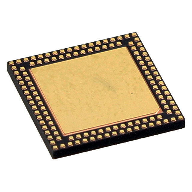
The flexible I/O matrix simplifies adaptation to various board layouts and system topologies. Programmable pin mapping permits pin multiplexing according to functional requirements, optimizing PCBs for both signal integrity and manufacturing scalability. The 100-pin TQFP package provides sufficient routing space while maintaining moderate footprint, a strategic balance for high-density industrial controls and multifunction logger nodes.
Electrical ratings support operation between 2.3V and 3.6V, compatible both with battery-powered designs and industrial-grade 3.3V domains. The extended temperature specification targets installations in thermal stress zones, such as outdoor control panels or motor drives.
A key insight emerges from the device’s holistic approach to microcontroller design: The blend of computational headroom, flexible peripherals, and robust memory management enables complex embedded solutions without resorting to external co-processors or fragmentation of system responsibilities. When prototyping scalable machine interfaces or integrated sensor gateways, this architectural convergence accelerates development cycles, promotes code portability, and enhances long-term maintainability—especially in sectors prioritizing field upgradeability and diagnostic transparency.
Key Features of PIC32MX370F512L-V/PF Microcontroller
Centered around the MIPS32® M4K® core, the PIC32MX370F512L-V/PF achieves a balance between computational throughput and code footprint efficiency. The five-stage pipeline design supports up to 80 MHz operation, delivering deterministic execution and maximizing instruction-level parallelism. Leveraging MIPS16e® code compression, the system reduces code size by approximately 40%, a tangible benefit for embedded applications facing tight memory constraints or requiring frequent firmware updates. This capability harmonizes with the device's extensive 512 KB of self-programmable Flash, enabling both robust primary application storage and flexibility for in-field upgrades. The 128 KB SRAM reserve matches typical requirements for sizeable buffer allocations in real-time data handling.
The presence of DSP-oriented instructions, such as single-cycle MAC and improved divide operations, differentiates the core for advanced control and embedded signal processing. These primitives mitigate latency in feedback loop applications, power electronics, and audio processing, where throughput and tight timing margins are non-negotiable. Empirical observation confirms the advantage in motor control algorithms, where reliance on fast arithmetic minimizes cycle consumption, supports higher control loop bandwidths, and unlocks new possibilities in embedded analytics.
Architecturally, the dedicated Prefetch Cache introduces a further optimization layer. By automatically pre-loading instructions and data, and supporting lockable lines, the microcontroller minimizes pipeline stalls associated with memory fetches. Predictive instruction prefetch works symbiotically with caching of constant and variable data, providing a seamless bridge between deterministic control code and data-intensive tasks. This approach translates into measurable improvements in time-critical operations, such as interrupt servicing and multi-threaded firmware.
The integrated analog subsystem underpins versatility in mixed-signal designs. A 10-bit, 1 Msps ADC delivers high-speed, multi-channel sampling for sensor interfacing, while support for up to 28 analog inputs allows dense signal aggregation on a single controller. The on-chip temperature sensor and flexible comparators are tailored for real-time diagnostics and threshold-based event detection, eliminating the need for supplementary analog hardware. In practical developments, this has enabled system consolidation, simplifying PCB layout and reducing bill-of-materials costs in industrial and scientific instrumentation.
Power management is addressed via dedicated Sleep and Idle modes, facilitating aggressive duty cycling without extensive software overhead. The retention of core context during transitions ensures fast wakeup, supporting both battery-sensitive and energy harvesting designs. This deliberate focus on low-power features extends operational longevity, a key parameter in remote and portable deployments.
A notable asset is the Charge Time Measurement Unit (CTMU), specifically engineered for high-resolution capacitive touch sensing. In conjunction with mTouch™ technology support, the CTMU streamlines the implementation of robust HMI interfaces, delivering precise response even in challenging electromagnetic environments. Practical integration reflects stable baseline tracking and immune performance in noisy settings, outperforming discrete implementation both in reliability and ease of tuning.
The PIC32MX370F512L-V/PF demonstrates a tightly engineered synergy between computational capacity, memory architecture, analog interfacing, and low-power operation. This convergence empowers the microcontroller to address the increasing demands of resource-constrained edge applications, where performance, integration, and deterministic response are all imperative. Its layered optimizations enable system architects to prototype and scale solutions across industrial, medical, and consumer segments with accelerated time-to-market and enduring functional resilience.
Power Management and Clocking in PIC32MX370F512L-V/PF
Power management and clocking in the PIC32MX370F512L-V/PF are architected to balance performance, energy efficiency, and robustness—core requirements for embedded control in dynamic environments. The device integrates multiple internal and external oscillator options, enabling seamless adaptation across various frequency domains. The on-chip PLL modules can dynamically scale core and peripheral clocks, supporting rapid mode-switching and clock divisibility. This configurability equips complex applications to optimally match system throughput with energy targets, yielding significant current savings during low activity periods.
Underlying these features is a resilient clock system. Fail-safe clock monitoring continuously checks primary oscillators, with automatic fallback to internal sources when anomalies are detected. This, paired with independent watchdog timers, forms a robust safety net for systems where interruption or misclocking has critical consequences. Practical deployments benefit from these layers of redundancy when managing remote or autonomous devices, where service interruptions can have operational or cost repercussions. The integration of Power-On Reset, Brown-Out Reset, and High Voltage Detect further extends system resilience, automatically enforcing safe states during supply transients or fault events—a necessity for applications deployed in unstable power environments.
Energy efficiency is further advanced by differentiated low-power modes. Sleep mode suspends CPU and most peripherals, dropping system currents to a minimum for deep power savings during inactivity. Idle mode provides granularity, halting only the CPU while peripherals run, optimizing trade-offs for scenarios such as sensor polling or timed communication windows. Real-world application frequently merges these features, cycling between active computation and controlled inactivity to minimize average power draw—particularly impactful in battery-operated or duty-cycled system designs.
Measurement data reinforce these architectural choices: typical dynamic current averages 0.5 mA/MHz under standard operation, with standby IPD current as low as 50 μA. Such characteristics enable deployment in energy-constrained contexts while maintaining high clock accuracy and operational integrity. Experience shows designs benefit most from an early assessment of power and clock requirements, leveraging flexible PLL settings and low-power modes. Strategic configuration—selecting optimal oscillator sources, scaling frequencies for task requirements, and using resets—builds both efficiency and resilience into embedded solutions.
A key insight emerges: robust clocking and power management are not simply peripheral features but foundational system enablers. Their engineered interplay within the PIC32MX370F512L-V/PF unlocks nuanced application tailoring, balancing latency, robustness, and autonomy. This layered approach ensures reliable operation and optimal power profiles, elevating system design possibilities across a range of embedded applications.
Peripheral Integration of PIC32MX370F512L-V/PF
Peripheral integration within the PIC32MX370F512L-V/PF is systematically architected for high versatility and scalability, targeting modern embedded solutions demanding simultaneous multi-domain interaction. The device’s peripheral fabric provides an instrumental foundation, serving both high-performance control and user interface requirements.
Graphics and Touch HMI capabilities are particularly robust. The Parallel Master Port (PMP) extends up to 34 independent pins, enabling direct interfacing to a wide range of TFT LCDs and external graphics accelerators. Support for mTouch™ capacitive sensing elevates the platform for intuitive human-machine interfaces (HMI), streamlined by low-latency I/O and minimal external component count. Often, direct connection to external frame buffers is feasible, minimizing glue logic in complex GUIs. PMP bandwidth, when paired with careful DMA utilization, unlocks flicker-free displays and responsive UI without overburdening the core, even under concurrent process loads.
Audio integration is refined for deterministic, high-throughput data movement. Dedicated I2S with left-justified, right-justified, and native USB audio interfaces supports multi-protocol streaming, critical in applications ranging from voice processing to high-fidelity media players. Real-time audio clock tuning and synchronization remove the historical burden of drift and noise, ensuring sample-exact alignment even during clock domain crossings. Hardware-driven SPI and I²C allow codec configuration or digital mixing with tight temporal control, key for minimizing audio latency in complex embedded designs. The peripheral’s deterministic nature is pivotal when pairing with wireless stacks, where interplay with Bluetooth or WiFi introduces additional timing requirements.
Advanced analog blocks are tailored for precise signal acquisition and monitoring under all power modes. The ADC, operable during device Sleep, supports asynchronous trigger modes—ideal for low-power sensing paradigms or event-driven acquisition in harsh environments. Dual comparators with programmable voltage references expand the analog front-end for power fail detection, motor control commutation, or touch interface baseline compensation. The integrated temperature sensor provides both functional safety and system self-monitoring, enhancing the device’s suitability in mission-critical or Class B safety contexts, where continuous health diagnostics are essential.
Timers and Output/Input modules are organized to maximize configurability and real-time processing efficiency. With multiple 16/32-bit timers, developers can implement advanced pulse generation (e.g., PWM for motor drives or lighting control) or assemble extended timebase architectures without recourse to firmware emulation. Output Compare and Input Capture modules, each with universal Peripheral Pin Select (PPS), adapt to variable board routing limitations and support rapid prototyping in evolving hardware environments. This pin multiplexing is further complemented by predictable interrupt response, essential for closed-loop control systems and time-sensitive communication protocols.
A communication interface suite is provisioned for dense, low-latency connectivity. The full-speed USB 2.0 On-The-Go (OTG) controller supports both host and device modes, enabling direct connection to peripherals or acting as an acquisition endpoint. Up to five independent UARTs, with LIN 2.1 and IrDA built-in, address not just legacy serial integration but also robust in-vehicle networking and industrial automation scenarios. Dual high-speed SPI controllers (up to 25 Mbps) facilitate serial memory expansion or sensor fusion with deterministic throughput, while I²C with SMBus support ensures reliability in system management and battery-monitoring networks. On-board RTCC (Real-Time Clock/Calendar) enables persistent scheduling, event logging, and power-fail resilience without external supervisor integration.
DMA and CRC resources are engineered for autonomous data movement and rapid integrity validation. The four general-purpose DMA channels perform auto data size detection and scatter-gather, substantially offloading the CPU during high-bandwidth transfers—especially notable in graphics refresh or complex sensor arrays. Two USB-specific DMA engines assure sustained throughput for isochronous or bulk endpoint streaming, a requirement for digital audio or imaging endpoints. Hardware CRC accelerates both memory integrity checks and real-time communications, adding a robust baseline for reliability in distributed or safety-critical designs.
Safety and compliance are programmed into the hardware domain. The embedded Class B library and IEC 60730 compliance features support critical function monitoring, such as clock, RAM, and flash diagnostics, with minimal software overhead. This hardware-software synergy is instrumental for white goods, HVAC controllers, or building automation equipment targeting certification-driven markets.
Strategically, the granularity and independence of each peripheral domain allow system-level designers to phase expansions or feature rollouts without platform migration. In practical deployment, it is evident that establishing early hardware abstractions—especially in PPS configuration and DMA channel allocation—streamlines iteration cycles and obviates later design bottlenecks. This modularity, coupled with advanced safety and reliability primitives, positions the PIC32MX370F512L-V/PF as a future-ready core for applications merging advanced UI, deterministic control, and secure connectivity under a unified silicon envelope.
Memory Architecture of PIC32MX370F512L-V/PF
PIC32MX370F512L-V/PF utilizes a sophisticated memory architecture designed to maximize performance, reliability, and flexibility in embedded systems. Central to its design is a unified 4 GB virtual address space, which enables both virtual and physical addressing while simplifying memory management. This architecture supports scalable and dynamic mapping of resources, minimizing fragmentation and allowing efficient utilization of available memory. The virtual addressing scheme also facilitates distinct user and kernel memory spaces, managed via hardware-enforced memory protection. By segregating these spaces, the architecture inherently mitigates risks arising from errant application code impacting critical system routines.
Flash memory implementation comprises a self-programming 512 KB array, structured with a 4 KB page size and 512-byte row boundaries. This fine granularity enables efficient erase and write cycles, optimizing in-application firmware updates. The device’s memory design ensures minimal disruption by isolating flash operations from ongoing SRAM usage, which is capped at 128 KB. The SRAM is logically divided for stack, heap, and static allocations, with clear demarcation enforced by the memory protection unit (MPU). This arrangement supports deterministic memory behavior, an essential property in real-time and safety-critical applications.
The inclusion of a 12 KB Boot Flash region provides a secure, immutable boot mechanism, essential for systems requiring resilient recovery and code integrity. Practical deployment illustrates that, by housing initial bootloader routines separately, it is possible to update main flash regions with minimal risk of rendering the device non-bootable. Such a strategy is common in field-upgradeable firmware, where robust failover pathways are necessary.
Cacheable memory regions deliver tangible performance benefits by mitigating access latency to frequently used code and data. Selective control over cacheability permits optimization tailored to the workload, enabling critical sections to benefit from reduced fetch cycles without incurring unnecessary overhead on non-critical areas. This modular cache control extends beyond performance, due to the potential for tight power management in constrained environments.
Robust bus exception handling detects and isolates memory access violations, supporting rapid diagnosis and recovery. Error handling registers track anomalies like illegal access or bus contention. Notably, such hardware-level diagnostics facilitate rapid root-cause analysis during development, and support in-field debugging through structured exception logging.
Key insights emerge from practical system integrations: leveraging both hardware memory protection and flexible memory mapping allows for secure implementation of multithreaded or real-time tasks, where memory isolation and deterministic response are paramount. Effective use of segmented SRAM, combined with judicious cache management, provides a balanced trade-off between throughput and predictability. At a system level, the unified memory model of the PIC32MX370F512L-V/PF delivers holistically managed, scalable resources — a necessity for modern embedded applications requiring both robustness and adaptability.
I/O and Pin Mapping Flexibility with PIC32MX370F512L-V/PF
The PIC32MX370F512L-V/PF microcontroller delivers exceptional pin mapping flexibility, supported by an I/O architecture engineered for adaptation across diverse hardware contexts. Available in up to 100-pin TQFP packages, as well as QFN and VTLA options, the device leverages industry-standard footprints to streamline integration into new or legacy designs. This breadth of packaging supports rapid prototyping cycles, facilitating the repurposing of standardized PCBs and sockets when platform requirements change over projects.
A central differentiator is the Peripheral Pin Select (PPS) system, which allows digital peripheral functions—including UART, SPI, I2C, PWM, and Timer inputs/outputs—to be reassigned to virtually any qualifying pin. PPS directly addresses the traditional bottleneck of fixed pinouts by enabling dynamic rerouting of signals during board layout and even in firmware updates. This intrinsic adaptability not only minimizes trace congestion and layer counts but also supports modular PCB topologies. For multi-functional platforms, PPS proves particularly valuable where peripheral allocation may evolve, enabling software-level reconfiguration without physical redesign.
Change notification input capability on all I/O pins further augments real-time responsiveness. Configuring pins as change notification sources enables efficient event-driven architectures, reducing polling overhead and advancing deterministic interrupt handling. Such features enhance the microcontroller’s suitability for control systems, industrial automation interfaces, and portable instrumentation. In practice, deploying change notification inputs minimizes latency in state-dependent routines while ensuring stability under asynchronous signal conditions.
Selective 5V tolerance across designated I/O pins creates reliable bridges with legacy systems and mixed-voltage domains, removing the need for external level shifters when interfacing with 5V logic components. This attribute simplifies BOM and layout complexity, allowing direct mating with off-board infrastructure or sensors operating at higher standards. It has proven effective in designs requiring seamless interoperability across automotive or industrial environments, where voltage standards may shift.
Further granularity emerges from software-driven options for open-drain mode, weak pull-up/pull-down resistors, and selectable Schmitt Trigger/TTL input thresholds. Open-drain configuration is instrumental in multi-master bus designs, fault-tolerant signaling, and direct LED drive circuits, where designers require explicit output control. Integrated weak pull-ups/pull-downs reduce reliance on discrete passives, leading to more compact and cost-effective boards. The choice between Schmitt Trigger and TTL inputs refines noise immunity and input sensitivity, proving especially relevant in mixed-signal environments or when interfacing with mechanical switches subject to bounce.
Navigating the configurability landscape, one perceives a strategic undercurrent: the PIC32MX370F512L’s I/O and pin mapping versatility is less about raw feature count and more about fostering hardware abstractions. Designs leveraging these features exhibit enhanced lifespan, reusability, and scalability. Through real deployment scenarios, such as transitioning prototypes to mass production or retrofitting existing control boards, the consistent experience is reduction in time-to-market and lowered risk when specification drift occurs.
Ultimately, the interplay of flexible pin mapping, robust interface options, and voltage domain accommodation constructs a comprehensive toolkit. The device stands as a prime enabler for platforms seeking both rapid adaptation and long-term maintainability, allowing configurable signal allocation to become a core element of intelligent hardware design.
Embedded Safety and Development Tools for PIC32MX370F512L-V/PF
Embedded safety and development strategies for the PIC32MX370F512L-V/PF emerge from a tightly integrated suite of hardware features and engineering workflows. The platform prioritizes reliability and rapid iteration through in-circuit and in-application programming capabilities. This permits on-board firmware modifications without physical removal, expediting both initial prototyping and iterative field updates. These methods enable a continuous refinement cycle, crucial in environments where minimizing downtime and increasing flexibility are non-negotiable.
At the silicon level, the four-wire enhanced JTAG interface, adhering to IEEE 1149.2, provides advanced debugging granularity. Unlimited program breakpoints and multiple data breakpoints facilitate fine-tuned code examination, allowing developers to trace nuanced operational flows and resolve multi-threaded or timing-sensitive anomalies. The extended breakpoint architecture ensures that run-state analysis scales from single-step debugging to complex interrupt-driven applications. This level of visibility is essential for isolating subtle bugs under real-world loading, significantly reducing time-to-resolution compared to more limited hardware debuggers.
The hardware’s code trace and boundary scan capabilities further emphasize design assurance and diagnostic throughput. Boundary scan enables comprehensive PCB-level connectivity checks, reducing the risk of latent soldering errors in production runs. Integrated support for MIPS EJTAG debugging deepens low-level firmware visibility, extending from register inspection to direct manipulation of instruction sequences. Development tool interoperability, unified by the industry-standard ICSP™ interface, accelerates toolchain setup and ensures seamless transitions between simulation, emulation, and physical device deployment.
System integrity is reinforced by built-in self-test and diagnostics functions, supporting IEC 60730 Class B compliance. These mechanisms execute at both boot and run-time intervals, autonomously verifying the integrity of critical peripherals, memory segments, and control logic. In practice, the modularity of these safety loops allows granular partitioning—individual tasks or state machines may invoke targeted diagnostics on-demand, enabling dynamic re-validation without full-system downtime. Implicitly, this fosters architectural designs where fault containment is inherent: the microcontroller can isolate and recover from transient or permanent faults, ultimately enhancing mission-critical system availability.
Carefully leveraging these embedded safety-centric features, development cycles achieve both velocity and resilience. The platform’s layered tool support harmonizes prototyping, debugging, validation, and certification efforts. Experience illustrates that maintaining clean separation between application logic and diagnostic routines, coupled with disciplined breakpoint management, yields maintainable codebases and simplifies regression workflows.
Neglecting these native capabilities compromises both efficiency and dependability, especially as product complexity escalates. Forward-looking designs incorporate systematic self-testing and granular debug hooks from the outset, establishing a foundation for both robust operation and expedient troubleshooting in real deployment. The PIC32MX370F512L-V/PF, through its tightly integrated safety and development tool ecosystem, exemplifies an architectural approach where hardware-centric support acts not as an afterthought, but as a core enabler for reliable, scalable, and certifiable embedded systems engineering.
Application Guidelines and Design Best Practices for PIC32MX370F512L-V/PF
Robust integration of the PIC32MX370F512L-V/PF hinges on a multi-layered approach to power distribution and signal integrity. Critical to stable performance is the deployment of high-frequency decoupling networks: parallel ceramic capacitors (0.1 μF with 0.01 μF), positioned within millimeters of each VDD and AVDD pin. This configuration drastically reduces local voltage fluctuations under dynamic load conditions and forms the first line of defense against transient switching noise, particularly at high core frequencies. For the internal regulator, the prescribed VCAP capacitor is non-negotiable for maintaining output stability—aluminum types are discouraged due to their high ESR characteristics, which can compromise transient response and introduce oscillatory behavior.
Pin state management is pivotal in safeguarding against unintended logic states and reducing spurious power dissipation. Configuring unused I/Os as outputs driven low achieves both EMI minimization and leakage control. Where input passivation is preferred—such as for diagnostic accessibility or design flexibility—using 1kΩ to 10kΩ pull-down resistors to Vss ensures a defined logic level and mitigates floating node susceptibility, a subtle yet common vector for noise ingress, particularly in dense layouts.
Oscillator circuit layout demands rigorous attention. Clock traces must remain as short as possible, with ground guard rings strategically routed to decouple sensitive signals from neighboring interference sources. Calculation of crystal load capacitors—aligned with manufacturer data and PCB stray capacitance—directly influences startup margins and sustained signal purity. Design oversights here frequently manifest as intermittent operation or degraded timing accuracy under temperature or supply variations, stressing the importance of both pre-silicon simulation and post-fabrication validation with precision instruments.
Leveraging the device’s 5V-tolerant digital I/Os enables straightforward interfacing in multi-voltage environments, streamlining direct bus connections. For non-5V tolerant pins, integration with mixed-voltage or floating external circuits necessitates the inclusion of dedicated level shifters or signal isolators. This is particularly vital in decentralized or modular deployments, such as hot-pluggable nodes, where voltage domain mismatches and unpredictable connection sequences are routine. Failing to provide this isolation is a frequent root cause for latent device failures brought on by EOS events or logic contention during power-up.
In environments characterized by high electromagnetic interference—typical of automotive control units or industrial automation—supplemental T-filters on supply rails prove invaluable. These filters attenuate conducted EMI and suppress cross-coupling through the power infrastructure, complementing the on-board decoupling strategy. Empirically, combining such hardware filters with disciplined grounding schemes elevates noise immunity margins, supporting compliance with stringent regulatory standards and enhancing system-level reliability.
A successful design process benefits from early, thorough system simulation and prototyping. Iterative analysis—oscilloscope-based eye diagram validation at oscillator nets, in-circuit monitoring of supply stability, and passive/active injection probing for EMI mapping—often reveals subtle layout dependencies and the efficacy of implemented countermeasures. Overlooking these adaptability elements can undermine yields and expose vulnerabilities in production, making seamless integration of these best practices central to both functional robustness and long-term maintainability.
Potential Equivalent/Replacement Models for PIC32MX370F512L-V/PF
Evaluating substitute or equivalent models for the PIC32MX370F512L-V/PF requires a methodical approach, beginning with internal architecture similarities within the PIC32MX family. The series groupings—PIC32MX330, PIC32MX350, PIC32MX370, PIC32MX430, PIC32MX450, and PIC32MX470—are anchored by consistent MIPS32 core architectures, similar peripheral frameworks, and standardized package options, supporting seamless migration across family variants. Central considerations include flash and RAM size, peripheral subset equivalence, and physical compatibility, as subtle changes in pinouts or feature sets may disrupt established software or PCB design.
Models such as PIC32MX350F256L offer a pragmatic downgrade in memory, reducing flash to 256 KB while maintaining the same TQFP-100 footprint and peripheral configuration. This facilitates cost reduction in applications where code size and data storage are moderate yet demands for CAN, UART, and timer modules persist. The PIC32MX330F064L pushes this optimization further; lower flash allocation (64 KB) and maintained peripheral parity address budget-constrained deployments, primarily where firmware complexity and sensor interfacing are predictable and bounded.
Migration toward enhanced connectivity and graphics capability situates the PIC32MX470F512L as a strategic upgrade path. With elevated CPU clock, improved core efficiency, integrated Ethernet MAC, and advanced SPI/Graphics controller support, this model aligns with scenarios requiring richer human-machine interfaces or networked communications. During hardware upgrades, one must recognize the subtle differences in analog subsystem implementations—such as ADC resolution—and additional high-speed communication modules that can introduce software adaptation requirements.
Pin mapping scrutiny remains essential throughout such transitions. Even minor discrepancies, such as shifted oscillator or Vref pins, can challenge production processes or system reliability. Comprehensive review of datasheet specifications, particularly electrical ratings and alternate pin functions, is required to forestall unexpected runtime conflicts or throughput bottlenecks. Layering this diligence with early schematics prototyping helps validate real-world compatibility prior to production.
Practical experience suggests that successful migration includes benchmarking peripheral drivers against new silicon, monitoring startup timing, and validating interrupt vectors. Occasional firmware adjustments are necessary when differing hardware errata emerge, especially in high-reliability instrumentation or mixed-signal control applications. Simplified bootloader update mechanisms and modular software architectures ease transition across product lines.
Integrating these insights supports sound engineering decision-making: selecting a true equivalent or superior replacement demands consideration beyond headline specifications, with integrated analysis of hardware, firmware, and manufacturing workflow interdependencies. This layered view yields robust system upgrades and avoids common pitfalls in the lifecycle evolution of PIC32MX-based products.
Conclusion
The PIC32MX370F512L-V/PF operates as a deeply integrated 32-bit MCU, leveraging the MIPS32 M4K core to deliver deterministic real-time performance. On-chip flash (512 KB) and SRAM (128 KB) enable responsive execution of complex firmware architectures, accommodating both control logic and data-intensive subsystems. Hardware multiply/divide capabilities and a high-speed peripheral bus facilitate low-latency responses in closed-loop systems, often critical for motion control, sensor fusion, and high-frequency signal processing domains.
Peripheral flexibility distinguishes this microcontroller in the embedded landscape. Up to 55 configurable digital I/O pins, multiple UART, SPI, and I2C channels, alongside industry-standard CAN 2.0b and USB 2.0 OTG functionality, permit seamless integration across layered communication topologies. Sophisticated analog support—featuring 16-channel, 10-bit ADC and multiple comparators—directly addresses mixed-signal requirements, such as real-time sensor interfacing in industrial automation or medical instrumentation. The on-chip graphics controller and touch sensing modules further condense electronics, eliminating the need for dedicated ICs in HMI or audio-visual implementations.
A primary concern in system-level design is minimizing both BOM complexity and PCB footprint. The comprehensive peripheral set and internal voltage regulation of the PIC32MX370F512L-V/PF support this goal, allowing for denser layouts and streamlined signaling. Practical deployment often reveals that distributed control schemes and sophisticated user interfaces can be realized effortlessly within the constraints of a single microcontroller, eliminating inter-processor synchronization and reducing the failure envelope.
The development ecosystem surrounding this device is mature and resilient. MPLAB X IDE integration, along with rapid prototyping hardware such as Curiosity Boards, accelerates product cycles and facilitates production-grade debugging via in-circuit emulation and trace features. Built-in support for memory protection and error correction underscores a commitment to functional safety, aligning with the stringent compliance regimes typical in industrial automation, automotive subsystems, and critical infrastructure monitoring.
Practical application scenarios emphasize tangible reductions in design iteration counts and field failure rates. Implementing robust bootloaders and adaptive firmware update mechanisms is simple, leveraging the controller’s Flash capabilities, and preempts costly recalls. Embedded designers routinely deploy this MCU in distributed sensor arrays, modular PLCs, and multi-protocol gateways, exploiting its deterministic response—especially under concurrent peripheral load—without sacrificing computational throughput.
The most effective exploitation of the PIC32MX370F512L-V/PF lies in deliberately architecting firmware for peripheral synergy, favoring event-driven design over traditional polling loops. This approach unlocks latent system performance, as peripheral interconnects and DMA engines decouple CPU intervention from routine tasks. Such design philosophies elevate not just throughput, but reliability in edge computing and data-acquisition systems.
The PIC32MX370F512L-V/PF represents an advanced convergence node in the modern embedded domain, offering substantial leverage for engineers seeking to balance performance, integration, and reliability. By facilitating scalable, safety-compliant, and maintainable products, it remains a crucial enabler for innovative designs in sectors where resource constraints and operational certainty define project viability.