


 >
>


Product Overview: Microchip PIC18F2580-I/SP
The Microchip PIC18F2580-I/SP exemplifies a refined integration of performance, connectivity, and memory management within the established constraints of an 8-bit microcontroller platform. Leveraging Microchip’s PIC18F architecture, this 28-pin SPDIP device achieves efficient instruction throughput by utilizing a pipelined RISC core optimized for up to 40 MHz operation. This core design minimizes instruction cycle bottlenecks, allowing deterministic response times—a critical requirement in embedded control systems where predictable behavior ensures reliability.
A key technical advantage lies in the microcontroller’s memory structure. With 32 KB of self-programmable flash and 1.5 KB of SRAM, the device enables flexible code deployment and efficient data buffering without external memory overheads. The inclusion of an endurance-enhanced EEPROM provides non-volatile storage for calibration or configuration parameters, supporting persistent application state across power cycles. These memory features support rapid development iteration, field upgrades, and long-term data retention typical of industrial and automotive applications.
Integrated peripherals position the PIC18F2580-I/SP as a versatile solution for interfacing requirements. The on-chip Enhanced CAN (ECAN) controller offers robust, standards-compliant communication for distributed network designs. This is complemented by interfaces including EUSART, SPI, and I2C, facilitating seamless connectivity across sensor modules, actuators, and other subsystems. The microcontroller’s analog-to-digital converter (ADC) and Capture/Compare/PWM (CCP) modules enable precise measurement and real-time control, crucial for energy management, motor control, or complex automation tasks.
Advanced power management allows for adaptive energy savings via selectable sleep modes, programmable brown-out resets, and a low-voltage programming interface. These features, when properly leveraged during system design, extend operational lifespans in battery-powered or power-sensitive deployments. Effective power strategy not only reduces thermal stresses but also enhances overall device dependability in harsh or remote environments.
Deployment scenarios benefit from the microcontroller’s capacity for rapid prototyping in through-hole development boards, thanks to its SPDIP packaging, while also ensuring low production costs. In practice, developers appreciate the streamlined configuration of subsystems via Microchip’s XC8 compiler and MPLAB X IDE, enabling swift migration from prototype to production. Iterative debugging, rapid parameter tuning, and field programming are routinely facilitated by the microcontroller’s bootloader capabilities and in-circuit serial programming support.
Careful system partitioning is advisable to prevent CAN bus latency from impinging on critical-control timing, particularly in multi-node networks where message prioritization is required. Additionally, selecting suitable oscillator configurations and optimizing interrupt routines allow developers to extract maximum real-time performance without sacrificing code maintainability. These nuances often determine the difference between marginal and robust system implementations.
Looking ahead, the PIC18F2580-I/SP’s architecture serves as an effective transitional platform—bridging traditional 8-bit processing with the emerging demands of networked, intelligent embedded systems. Its blend of deterministic execution, flexible peripherals, and scalable memory offers a pragmatic pathway for engineers seeking to balance design complexity, cost, and long-term maintainability within a single microcontroller solution.
Core Architecture and Performance of the PIC18F2580-I/SP
The PIC18F2580-I/SP leverages an 8-bit enhanced RISC core, which utilizes the Harvard architecture to realize distinct program and data memory buses. This separation fundamentally optimizes instruction fetch and data access phases, eliminating potential memory access bottlenecks and enabling parallelism that is pivotal for real-time embedded systems. The precise demarcation between instruction and data paths permits simultaneous data transfers and code execution, minimizing latency during critical operations.
The instruction set architecture is purpose-built for high-level C compilation, supporting advanced control flow and arithmetic routines without incurring excessive overhead. Designers benefit from predictable, single-cycle instruction timing, which is essential for deterministic system behavior in timing-sensitive applications. Extensions within the instruction set further enhance programmability when dealing with complex logic or protocols, such as those found in automotive or industrial controller environments.
Central to the execution efficiency is an integrated 8x8 hardware multiplier, completing multiply operations in a single clock cycle. This hardware feature transforms the microcontroller’s capacity for signal processing tasks, such as digital filtering or fast sensor data analysis, making it well-suited for pulse-width modulation control loops or motor algorithms. Bypassing software-level multiplication sharply reduces processing time and power consumption during intensive tasks.
The interrupt controller is finely tuned, supporting multiple priority levels for nested and vectored interrupt handling. This hierarchical scheme allows time-critical interrupts to preempt less urgent ones, maintaining system responsiveness under sustained or bursty event conditions. Practical scenarios benefit from this robust structure, such as CAN protocol stack servicing, where reception and transmission need tight timing guarantees. The controller’s architecture allows for tailored prioritization strategies according to operational risk factors and real-world deployment conditions.
Performance is anchored by the device’s ability to reach up to 40 MHz clock speeds, facilitated by an internal phase-locked loop. This capability enables the execution of sophisticated algorithmic routines and concurrent peripheral management, meeting requirements for data-heavy or cycle-hungry functions. During in-circuit deployment, this headroom allows adaptation to variable workload, whether scaling protocol handling or synchronizing high-speed I/O events.
From a design perspective, integrating fine control over low-level memory access, arithmetic acceleration, and real-time event management creates a scalable platform. The architecture’s careful balance between enhanced instruction flexibility, high-speed arithmetic, and interrupt agility yields significant advantages for developers aiming to maximize throughput without excessive resource overhead. This design philosophy positions the PIC18F2580-I/SP as a robust component for applications demanding precise control, predictable timing, and compact code implementation.
Oscillator Options, Clock Control, and Power Management in the PIC18F2580-I/SP
Oscillator architecture in the PIC18F2580-I/SP microcontroller demonstrates high configurability tailored for robust system design. The availability of ten distinct oscillator modes—including multiple external crystal and resonator interfaces supporting frequencies up to 40 MHz, external RC configurations, and clock input options—enables custom tuning to match application-specific timing, frequency accuracy, and cost demands. The internal oscillator block further expands possibilities, presenting eight selectable frequencies ranging from 31 kHz to 8 MHz, and a Phase-Locked Loop (PLL) multiplier that extends usable clock rates to 32 MHz for performance-critical tasks. Calibration circuitry incorporated in the internal oscillator fosters precise baseline timings, which is fundamental when operating in environments susceptible to temperature variation or supply disturbances. Selection between internal and external sources by firmware or hardware, and real-time switching capabilities, facilitate seamless adaptation to changing requirements across operational states.
From a systems perspective, frequency management directly impacts electromagnetic compatibility (EMC). For example, shifting clock sources or dynamically scaling frequency with the PLL can minimize emissions in noise-sensitive designs. In prototyping, frequency adjustments were used to reduce radiated emissions below regulatory thresholds, allowing integration without redesign of board-level shielding or filtering. Engineers benefit from an adaptable platform that can shift priorities from throughput to compliance with minimal firmware intervention.
Power management is interwoven into the oscillation strategy, promoting exceptionally low current draw through three primary operating states: Run, Idle, and Sleep. Strategies such as leveraging the IDLEN bit and Secondary Clock Select (SCS) register enable efficient transitions and real-time clock switching, reducing the active core power when full speed is unnecessary. The microcontroller’s ability to attain sub-microamp consumption in Sleep and Idle states—empirically validated by measuring sleep currents under various supply conditions—is instrumental for battery-powered sensors and portable instrumentation. Firmware-controlled clock gating ensures that peripherals not required by application logic are systematically down-clocked or disabled, optimizing overall energy budget.
Rapid wakeup from low-power modes is crucial for data acquisition, control, or monitoring systems requiring both responsiveness and prolonged operational life. The hardware implementation minimizes latency to restore system clocks and peripheral logic, supporting predictable interrupt response pathways. In practice, firmware leveraging on-the-fly clock switching has minimized energy usage during communication intervals while maintaining instantaneous activation on external stimulus—demonstrating the value of granular clock domain control in time-sensitive applications.
When integrating oscillator and power-management features, attention to layout, component selection, and supply decoupling further amplifies system reliability. Using short traces for crystal connections and low ESR capacitors enhanced startup robustness and limited phase jitter. These design details, when coupled with firmware that deliberately tailors operational modes to the application profile, realize the full spectrum of flexibility the PIC18F2580-I/SP offers. As system complexity and energy-conservation demands intensify, the ability to orchestrate diverse oscillator sources and power regimes translates into tangible benefits for designers pursuing optimal efficiency and compliance across a broad range of embedded deployments.
Memory Organization and Endurance Features of the PIC18F2580-I/SP
The PIC18F2580-I/SP features a balanced memory architecture tailored for reliable embedded control. Its 32 KB Enhanced Flash program memory is engineered for in-circuit reprogrammability, supporting dynamic firmware updates without the need for external programming interfaces. High-endurance Flash technology, rated for 100,000 program/erase cycles, sustains rigorous code development cycles and in-field reconfiguration, crucial for systems evolving through iterative deployment or remote updates. The 256-byte EEPROM complements this with up to 1,000,000 endurance cycles, well suited for persistent storage of configuration parameters, calibration constants, or runtime logs, especially in installations where operational stability over decades is essential. With data retention exceeding 40 years, both memory types align well with safety-critical and industrial automation requirements, where infrequent power cycling and nonvolatile robustness are paramount.
The Harvard architecture fundamentally enhances concurrent accessibility: separate data and program buses enable genuinely parallel instruction and data fetches. This sharpens real-time responsiveness, allowing the microcontroller to efficiently handle sensor fusion, rapid control loops, and high-throughput communication stacks. The memory-mapped design further mitigates pipeline stalls during heavy data movement, feeding deterministic execution timing—a necessity in domains like automotive CAN networks or closed-loop motor drives.
Self-programming features extend the operational lifetime by facilitating secure bootloader implementations and authenticated firmware upgrades, even post-deployment. Firmware updates via CAN or UART, with on-chip integrity checks, support a layered defense against code corruption or tampering—a strategy increasingly relevant for distributed control nodes and field-level IoT endpoints. Practical integration reveals that careful partitioning of Flash and EEPROM usage prevents reliability bottlenecks: firmware and core routines reside in protected Flash sectors, while EEPROM efficiently manages high-frequency writes by employing wear-leveling or redundant variable schemes to prolong endurance.
A nuanced observation lies in the engineering trade-off between RAM size and nonvolatile memory. With 1536 bytes of RAM, the device supports modest real-time data sets without risking overflow-induced exceptions during typical control, filtering, or protocol tasks. Leveraging Flash for infrequent code patches and EEPROM for evolving system parameters, while keeping runtime buffers in RAM, establishes a clear operational delineation, optimizing both processing speed and architectural longevity.
In summary, the PIC18F2580-I/SP's memory organization delivers a highly adaptable persistence blueprint, seamlessly integrating endurance, real-time performance, and in-application programmability. These features collectively position the device as an optimal choice in scenarios demanding resilient operation, modular updates, and robust lifecycle predictability.
Peripheral Highlights of the PIC18F2580-I/SP
Versatility is embedded in the architectural DNA of the PIC18F2580-I/SP through its comprehensive peripheral set, which empowers robust integration across varied embedded systems. At the heart of serial communication support lies the Master Synchronous Serial Port (MSSP), engineered for seamless operation with both SPI and I2C protocols in either master or slave configurations. This duality enables immediate adaptation to a wide spectrum of sensor, EEPROM, and peripheral interconnects, minimizing component count and facilitating rapid system design pivots. The predictable timing and tightly managed bus arbitration mechanisms mitigate common implementation pitfalls encountered in noisy environments or when hot-swapping devices.
The Enhanced USART module expands the communication reach beyond synchronous protocols, featuring direct hardware support for RS-232, RS-485, and automotive LIN/J2602 interfaces. Features such as auto-baud rate detection and addressable wake-on-activity are especially beneficial in power-critical networks and distributed control systems, ensuring rapid link establishment and minimizing firmware overhead. The EUSART’s noise rejection and framing error handling, further augmented by hardware interrupt structuring, yield resilient links even where electrical disturbances and variable baud rates are present—realized advantageously in mobile data logging or remote sensing applications.
A precise 10-bit analog-to-digital converter with up to eight multiplexed channels extends the PIC18F2580-I/SP’s reach into the analog domain, supporting programmable acquisition windows and enabling sampling during device Sleep mode. This combination of flexibility and ultra-low power operation elevates suitability for battery-sensitive applications such as portable diagnostics or environmental monitors. Hardware-driven averaging and the ability to synchronize acquisition events with timers or CCP outputs can drastically reduce signal aliasing, improving measurement integrity in noise-prone installations.
Timing and control are reinforced by the inclusion of a single Capture/Compare/PWM (CCP) module. This subsystem is tuned for nuanced motor control, pulse generation, and event timing synchronization, where the interplay between high-resolution timers and programmable output stages supports complex drive patterns or frequency modulation tasks. Pairing the CCP capabilities with a structured interrupt scheme allows for real-time event response, a necessity in precision motion systems and safety-critical automation.
Analog signal conditioning is further augmented by dual analog comparators equipped with input multiplexing and internal voltage reference capability. This facilitates rapid development of window-discriminator circuits, zero-cross detection, or safety interlocks without external circuitry, conserving PCB space and reducing BOM complexity. Input multiplexing broadens practical flexibility, enabling the hardware to perform adaptive thresholding and fail-safe detection across multiple signal domains.
A portfolio of hardware timers—spanning 8- and 16-bit widths—and interrupt-driven event handling underpins deterministic system scheduling. These timers offer reliable pulse-width modulation, runtime diagnostics, and watchdog services, bolstering fault tolerance and efficiency in embedded control loops. The tight integration of interrupt sources ensures that both periodic and asynchronous events can be serviced with minimal processor latency, a core requirement for responsive industrial profiles.
Maximum I/O drive capability stands out—the ability for each digital pin to source or sink up to 25 mA eliminates the need for buffer stages when controlling moderate loads. Direct LED arrays, relays, or solenoids can be actuated quickly and efficiently, allowing for streamlined hardware layouts and faster prototyping cycles. This characteristic directly reduces design risk during load integration phases and offers a foundation for scalable digital output expansion.
The synthesizing factor across these peripherals is the engineered balance between configurability, performance, and ease of integration. The PIC18F2580-I/SP achieves this without sacrificing reliability, enabling design teams to iterate across a spectrum of embedded solutions with minimal codebase or hardware churn and offering tangible gains in development velocity and maintainability. This convergence of layered peripheral utility, deterministic behavior, and electrical robustness positions the device as a strategic cornerstone for applications that demand adaptability without compromise.
ECAN Technology and Communication Interfaces in the PIC18F2580-I/SP
In-depth analysis of the PIC18F2580-I/SP reveals the integration of Enhanced CAN (ECAN) technology as a cornerstone for modern embedded networking tasks. The ECAN module’s compliance with CAN 2.0B ensures interoperability across a range of automotive and industrial systems that rely on established fieldbus standards for real-time communication. Its bit rate support up to 1 Mbps directly addresses throughput demands typical of high-velocity data environments.
The architecture adopts a multi-buffered schema: three prioritized transmit buffers, complemented by two dedicated receive buffers. This arrangement minimizes software intervention by decoupling transmission scheduling from reception handling, reducing interrupt latency and enhancing determinism. The transmit buffers prioritize critical messages without blocking lower-priority frames, a crucial aspect when addressing mixed traffic types such as command/control and diagnostic data over a single bus. In high-frequency polling scenarios, this buffer configuration maintains throughput consistency, even when message bursts occur from distributed nodes.
Acceptance filtering further elevates bus efficiency. With sixteen independently programmable filters and three full 29-bit masks, the module isolates relevant frames at the hardware level. Configurable filter-to-mask associations enable dynamic re-routing or message arbitration based on evolving network conditions—an asset in Heavily loaded buses, especially where network segmentation and logical node grouping become necessary. This hardware-level filtering significantly relieves the CPU from software message parsing duties, translating to improved response times and lower overall system power consumption. Situations involving diagnostic snapshots during live operation benefit substantially, as only pertinent identifiers reach the MCU core, enabling precise real-time monitoring.
Advanced error management mechanisms embedded in the ECAN module—including automated bus-off recovery, error counters, and event interrupts—strengthen system resilience. These functions maintain bus integrity and allow for rapid diagnosis of fault conditions, which is especially critical in safety-related automation clusters or automotive ECUs conforming to ISO 26262 guidelines.
DeviceNet™ compatibility adds another layer of practical utility, streamlining integration into industrial topologies standardized around this protocol. Field experience shows that dynamic filter association, coupled with legacy compatibility modes, facilitates seamless migration from older CAN solutions. Upgrading legacy platforms becomes feasible without a wholesale redesign of the communication backbone, which is particularly valuable in cost-sensitive automation sectors.
The presence of EUSART and MSSP (supporting both I2C and SPI) on the same MCU serves a pivotal role in cross-domain applications. It enables gateways combining CAN, UART, and serial-peripheral interfaces on a unified silicon platform. This convergence reduces BOM complexity and fosters design flexibility, as complete protocol bridging can be performed within a single firmware context. Distributed sensor networks, motor controllers, and node-level communications in modular machinery illustrate application domains where such tight multi-protocol integration has yielded measurable efficiency gains and faster development cycles.
A nuanced perspective recognizes the PIC18F2580-I/SP not just as an aggregator of communication suites, but as an enabler of deterministic, scalable bus architectures. Its emphasis on hardware offload—across filtering, arbitration, and error management—allows network-centric products to achieve both higher reliability and real-time responsiveness. Design iterations incorporating intelligent buffer handling and dynamic filtering demonstrate lower CPU utilization, allowing attention to be redirected to application logic, advanced diagnostics, or predictive maintenance algorithms. This allocation difference often marks the gap between generic controllers and those optimized for tightly-coupled, mission-critical environments.
Programming, Debug, and Application Integration for the PIC18F2580-I/SP
Programming, debugging, and application integration for the PIC18F2580-I/SP require careful consideration of both hardware capabilities and development workflow to achieve robust embedded solutions. The device’s In-Circuit Serial Programming (ICSP™) interface reduces system complexity by enabling firmware updates via only two dedicated pins, minimizing the need for additional components and facilitating both initial programming on the production line and in-field updates after deployment. This streamlined access is essential in designs where board space is at a premium or post-assembly programming flexibility must be maintained.
The inclusion of In-Circuit Debug (ICD) support elevates system observability, enabling real-time code execution monitoring and step-by-step debugging through MPLAB IDE integration. This capability provides a deterministic view of internal register states and on-the-fly variable inspection—leading to faster fault isolation, root cause analysis, and optimization loops even as the target device remains embedded in its operational environment. ICD’s non-intrusive operation ensures minimal interruption to system timing, which is critical in real-time control or communication applications where temporal determinism is non-negotiable.
Security mechanisms, such as code read protection and boot block segmentation, address the growing need for intellectual property safeguarding and firmware integrity during field updates. By leveraging boot block segmentation, system architects can partition critical bootloader regions from the main application code, ensuring that even if the primary application is updated remotely, the trusted bootloader remains immutable. In practical deployments, this mechanism forms the groundwork for secure over-the-air or remote update workflows and mitigates risk from both inadvertent corruption and deliberate tampering.
Integration with Microchip's comprehensive development ecosystem—including evaluation kits, reference designs, and MPLAB IDE—enables rapid prototyping, iterative code development, and automated testing. The ecosystem substantially lowers implementation barriers, facilitating migration from proof-of-concept to production-grade systems. In practice, leveraging these resources accelerates time-to-market, reduces debugging effort, and permits thorough validation of both core microcontroller functionality and peripheral interfaces. Notably, embedded engineers benefit from software tools that provide intelligent build configurations, device-aware static analysis, and seamless toolchain upgrades, all contributing to greater design confidence and maintainability.
Effective deployment of the PIC18F2580-I/SP unlocks competitive differentiation through design agility, secure field programmability, and transparent development flows. This microcontroller family, when utilized with its full complement of programming, debugging, and security features, forms a foundation for resilient, scalable embedded applications, especially where long product lifecycles and post-deployment flexibility command priority. Field experiences consistently demonstrate that engineered attention to these core pillars reduces lifecycle maintenance costs, minimizes unscheduled downtime, and fosters a modular architecture more adaptable to evolving project requirements.
Pinout and Package Considerations for the PIC18F2580-I/SP
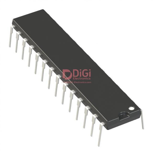
Pinout and package selection significantly impact system integration and board-level design, particularly for the PIC18F2580-I/SP. The device’s 28-pin SPDIP package streamlines prototyping workflows and accelerates iteration cycles. This standard footprint supports straightforward manual soldering and socket usage, facilitating rapid hardware validation without reflow soldering constraints typical of surface-mount devices. Engineers often exploit SPDIP’s through-hole format for direct breadboarding or socket insertion, reducing risk exposure during early-stage development.
Careful mapping of signal assignments forms the backbone of stable system operation. The device organizes its I/O into three bi-directional ports, with pins multiplexing a range of analog, digital, and communication functions. Understanding peripheral sharing is critical to prevent contention; for example, analog input channels frequently share pins with digital lines or communication signals, mandating precise configuration at both schematic capture and firmware levels. Board designers must factor in potential cross-domain interference—analog traces adjacent to high-speed digital lines can introduce crosstalk, requiring routing discipline or strategic use of ground planes and guard traces. During schematic review, particular scrutiny must be applied to all pins with multiplexed roles, as these often underpin CAN or UART connectivity in automotive and industrial settings.
Robust system power distribution is contingent on correct decoupling and reference connections. The required VDD and VSS lines must maintain low-impedance paths via appropriate decoupling capacitors positioned close to the package. The presence of separate AVDD and AVSS pins isolates analog subsystem noise from digital domains, an architectural advantage when sampling precision is paramount. Ensuring short, wide traces and tight coupling between analog power and ground significantly improves ADC accuracy and overall system noise immunity. Misrouting these signals or omitting recommended decoupling frequently manifests as increased conversion error during field testing.
Essential functional pins—including MCLR (external reset), oscillator drive inputs, and programming/debug interfaces—demand early allocation in PCB layout. Assigning accessible locations for the ICSP interface streamlines code upload and diagnostic cycles, especially during ongoing firmware changes. The oscillator configuration, whether via crystal or external clock, anchors the system timing budget; stray capacitance, trace symmetry, and crystal loading need validation to achieve reliable startup and frequency tolerance, particularly in communication-heavy deployments.
Experienced practitioners anticipate common board-level oversights such as floating configuration pins or inadvertent shorting of critical supply lines beneath the SPDIP body. Optimized footprints allow for test-point placement and voltage monitoring without risking solder joint reliability. When transitioning from SPDIP prototypes to production surface-mount variants, pin compatibility and hardware abstraction are maintained by mirroring net assignments and validation constraints discovered during the initial SPDIP phase.
Overall, effective exploitation of the PIC18F2580-I/SP’s package features and nuanced pinout directly correlates to streamlined bring-up and reduced revision cycles. Mastery of these low-level considerations underpins confidence in more complex designs and accelerates the move from proof-of-concept to robust system deployment.
Power Supply, Reset, and Robustness Features of the PIC18F2580-I/SP
Power supply integrity in the PIC18F2580-I/SP is achieved through a cohesive integration of programmable brown-out reset (BOR), power-on reset, and a highly configurable watchdog timer. Brown-out reset functions through threshold detection circuits that continuously monitor Vdd, initiating a controlled reset whenever voltage drops below user-defined limits. This real-time supervision counteracts erratic microcontroller behavior during supply sags, especially vital in installations subject to load transients or unstable power sources. The programmable aspect enables precise adaptation to system-level profiles, reducing false triggers and maximizing uptime in variable supply scenarios.
The power-on reset subsystem initializes the device to a known state at startup, independent of ramp rate or residual voltages. This approach prevents partial code execution and unpredictable peripheral states that could arise from slow or noisy power application, ensuring deterministic boot processes. The hardware watchdog timer, equipped with extended timeout adjustments, acts as a temporal guardian over software execution by resetting the core when normal code flow is lost or locked. Selection of timeout windows allows for balancing between aggressive fault recovery and the needs of longer, computation-heavy cycles typical in advanced control code modules.
PCB layout and external decoupling capacitors are not just supporting elements—they are integral for suppressing high-frequency supply noise and voltage dips, which are common in EMI-prone environments. Placing low-ESR capacitors near the device supply pins minimizes ground bounce and ensures consistent analog reference levels, crucial for predictable performance in sensor-driven or analog-mixed designs. Attention to trace routing, ground plane integrity, and minimizing EMI loop areas directly correlates to the realization of the microcontroller's inherent noise robustness.
All I/O pins are fortified with on-chip ESD and overvoltage protection networks. These protective elements absorb and shunt transient energy, reducing circuit vulnerability to inadvertent discharges and field-level surges. The resilient I/O structure allows deployment in harsh automotive or industrial applications, where connector handling and cable interfaces represent frequent sources of electrical stress. Design best practices—such as grounding unused pins and proper shielding—further extend the baseline protection, demonstrating that robustness is not solely a hardware property but a system-level achievement.
Task-critical domains such as mission control, automotive body electronics, and industrial automation benefit markedly from these collective safeguards. The layered architecture of power, reset, and protection mechanisms ensures that operational predictability is maintained even under compound fault conditions. The PIC18F2580-I/SP's power integrity and resilience features, when implemented alongside informed PCB and system design, substantially increase reliability margins and sustain functional safety requirements unique to high-dependability deployments. Recognizing that these mechanisms function optimally only within a well-engineered context highlights the interplay between silicon features and system architecture—a nuance often underappreciated in superficial evaluations.
Potential Equivalent/Replacement Models for the PIC18F2580-I/SP
Evaluating replacement options for the PIC18F2580-I/SP in embedded system design requires systematic assessment of core architectural features and peripheral configurations. At the microcontroller's foundation, compatibility with existing codebases, debugging tools, and established bus architectures is essential for seamless transition. Matching instruction sets and peripheral registers between candidate devices ensures software reusability and minimizes firmware adaptation overhead.
The PIC18F2480 offers a close substitute, maintaining identical CPU architecture and communication interface capabilities—including CAN modules—while reducing Flash memory to 16 KB and analog input count. This variant aligns with resource-sensitive designs where code size and analog channel usage are limited. Practical deployment of the 2480 is observed in streamlined sensor interfaces and compact control loops, benefiting from lower Bill-of-Materials cost in high-volume applications.
For systems demanding broader connectivity, PIC18F4580 and PIC18F4480 extend the feature matrix substantially. The increased pin count and additional analog channels directly address expanded signal acquisition and actuator multiplexing needs. Integration of dual CCP/ECCP modules in these models enables simultaneous high-resolution PWM waveform generation and advanced timing features, suited to multi-motor automation or power stage management scenarios. The parallel slave port adds efficient data exchange capabilities in designs interfacing with external logic or legacy parallel peripherals. Careful mapping of I/O requirements to available ports greatly simplifies PCB layout and system scaling.
Voltage flexibility emerges as a decisive factor in designs subject to variable power environments. The PIC18LF2580’s operation across a 2.0V–5.5V supply range facilitates compatibility with battery-powered or low-voltage regulated domains, eliminating constraints imposed by standard voltage thresholds. In field deployments exposed to strict power budgets or supply fluctuations, low-voltage variants maintain operational robustness without redesigning power distribution subsystems.
Selecting the optimal model involves correlating application-specific constraints—memory allocation, I/O density, analog front-end needs, and physical package dimensions—with device feature sets. Early-stage prototyping has demonstrated that direct pin- and peripheral mapping between members of the PIC18F family accelerates migration and reduces risk of functional discrepancies. Strategic use of larger packages unlocks modular expansion, while scaling down to memory-efficient options optimizes for cost and size-critical profiles.
A nuanced approach to replacement considers not only feature parity but also latent system capabilities unlocked by peripheral enhancements, voltage adaptability, or interface multiplexing. Leveraging these subtle distinctions drives greater architectural longevity and design agility, ensuring that platform transitions are both effective and future-proof.
Conclusion
The Microchip PIC18F2580-I/SP microcontroller stands at the intersection of robust architecture and flexible integration, making it especially suited for embedded control tasks in automotive, industrial, and distributed system environments. Central to its value proposition is the high-instruction-throughput core, built on Microchip's PIC18 family CISC architecture, which combines a deterministic response with interrupt prioritization. This enables low-latency execution for real-time control, precise event handling, and streamlined code modularity—critical characteristics for high-reliability applications where predictable behavior governs system safety and performance.
Peripheral integration on the PIC18F2580-I/SP reflects a thorough consideration of domain requirements. The on-chip CAN controller, conforming to ISO 11898, provides seamless networking for distributed electronic control units, a frequent demand in modern automotive and industrial automation. In practical deployment, the independent CAN buffer management and error-correction capabilities have proven to minimize diagnostic complexity and facilitate rapid system fault recovery, even under heavy bus traffic. The device’s broad range of peripherals—including ADCs, CCP modules, and industry-standard communication interfaces like SPI, I²C, and USART—eliminates the need for supplementary components, reducing BOM costs and PCB real estate, while accelerating product iteration cycles.
Power management circuitry underscores the device’s adaptability. Features such as enhanced sleep and idle modes, programmable brown-out detection, and integrated watchdog not only lower standby power consumption but also safeguard system reliability against supply fluctuations and software deadlocks. In field applications where supply instability or electromagnetic noise is prevalent, the MCU’s rapid wake-up from low-power states and resilient supervisory elements have been advantageous for extending operational lifetime and maintaining persistent device uptime.
From a development perspective, the maturity of Microchip’s toolchain—spanning MPLAB IDE, XC8 compiler support, exhaustive reference designs, and migration pathways with extensive package and memory variant compatibility—streamlines the transition from prototype to volume deployment. This comprehensive ecosystem reduces learning curves and mitigates integration risks when transitioning legacy designs or scaling system complexity.
A distinguishing aspect of the PIC18F2580-I/SP lies in the balance it achieves between feature granularity and system robustness. The flexible pin multiplexing, broad voltage operating range, and proven backward compatibility model ensure that hardware reusability and design longevity are not compromised, even as functional requirements evolve. Such engineering-centric characteristics anchor the device’s relevance in both long-term platform life cycles and rapid development snapshots, supporting sustainable embedded solution roadmaps without sacrificing performance or reliability.
Key insights arise from observing its deployment in networked sensor clusters, motor controllers, and low-complexity gateways: the MCU’s predictable interrupt handling, high peripheral bandwidth, and stable communication layers establish a dependable infrastructure for escalating application sophistication, minimizing the friction of architectural upgrades and maintenance interventions. The PIC18F2580-I/SP thus defines itself not just through its specification sheet, but through accumulated field experience, offering a tangible foundation for reliable and forward-compatible embedded system designs.


