>
>


Product Overview of the AT24C01C-SSHM-T
The AT24C01C-SSHM-T stands out as a compact, nonvolatile serial EEPROM implementing a 1 Kbit memory array organized for byte-level and page-level access. Deployed in an 8-lead SOIC package, this device leverages the established I²C bus architecture, simplifying board layout and minimizing pin requirements. Its interface logic is highly interoperable with standard I²C controllers, supporting both 100 kHz (standard) and 400 kHz (fast-mode) operation for scalable performance across a spectrum of applications.
This EEPROM’s wide operating voltage range from 1.7V to 5.5V optimizes compatibility with both legacy and low-power digital platforms, enhancing flexibility during system-level power rail selection. Write endurance, exceeding one million cycles per memory cell, and data retention of at least 100 years underscore the device’s reliability, even under stringent industrial operating profiles. The hardware write-protect feature, accessible through the WP pin, is essential for safeguarding critical data in environments exposed to accidental writes or unauthorized code execution.
At the circuit integration level, pull-up resistors must be included on both the SDA (Serial Data) and SCL (Serial Clock) lines to maintain logic-level integrity, particularly in multi-slave topologies. When bus arbitration or hot-swapping is required, the device’s robust ESD protection and input filter characteristics mitigate issues arising from electrical transients and signal cross-talk. The package’s thermal stability further facilitates placement decisions on densely populated PCBs, allowing for co-location with heat-generating components without compromising data integrity.
In deployment scenarios, the AT24C01C-SSHM-T is routinely selected for storing configuration tables, calibration coefficients, and device identification strings in embedded control modules, where frequent updates coexist with the demand for persistent storage. The fine granularity of its memory structure enables efficient handling of parameter blocks, firmware version tracking, or feature enablement flags, reducing overhead typically associated with larger, block-oriented memories.
Designers favor this device in initialization and self-test routines, where code must retrieve or update operational parameters at power-up without incurring processor wait states. Its minimal standby current reduces baseline system power consumption, supporting battery-operated and energy-harvesting applications. System validation procedures benefit from consistent power-up behavior due to the memory’s immunity to brownout-induced corruption.
From an engineering perspective, balancing the I²C pull-up resistor value is critical. Lower values enhance noise immunity but increase power consumption on the bus, while higher values reduce current draw but risk timing violations on faster mode clocks. Proper PCB trace routing for SDA and SCL also reduces likelihood of spurious writes or clock stretching, particularly in electrically noisy systems. For firmware integration, standard I²C driver libraries can be customized to implement retry mechanisms and page boundary checks, maximizing write throughput while avoiding page wrap-around errors that can silently corrupt adjacent storage.
Fundamentally, the AT24C01C-SSHM-T exemplifies the optimal intersection of density, durability, and interface simplicity. It supports a modular design philosophy, enabling repeated reuse across product lines without costly redesign, and its predictable behavior under real-world disturbances underpins robust, maintainable embedded architectures. This device’s enduring appeal lies in the ability to incorporate secure, high-reliability nonvolatile memory into space-constrained or power-sensitive designs without trade-offs in integration effort or interface complexity.
Key Features and Advantages of the AT24C01C-SSHM-T
The AT24C01C-SSHM-T integrates core EEPROM attributes with refined power and performance specifications, catering to embedded applications where operational efficiency and robust data integrity are paramount. Its maximum active current of 3 mA and standby current of 6 µA constitute a critical differentiator in circuits demanding minimal quiescent power, supporting platforms that must maximize battery life or maintain 24/7 responsiveness.
The device’s multi-speed I²C interface—supporting 100 kHz, 400 kHz, and 1 MHz FM+—aligns to the increasing system requirements for higher throughput without sacrificing signal integrity. In practice, this enables predictable scaling from legacy controllers to new generations with faster serial buses. Fast Mode Plus operation proves particularly relevant in time-sensitive or bandwidth-constrained designs, where swift parameter updates and batch configuration reads are essential.
Underlying reliability mechanisms set the AT24C01C-SSHM-T apart for long-life deployments. The bit-level endurance of over one million write cycles, paired with a century-scale data retention, ensures viability for both logging and calibration data storage in industrial controls, consumer wearables, and automotive subsystems. Deployed in environments with exposure to transient noise or variable supply voltages, the inclusion of Schmitt-triggered inputs and spike suppression filters provides measurable improvements to data accuracy during I²C transactions, reducing inadvertent state changes due to bus disturbances.
From a data protection perspective, hardware-level write-protect functionality offers seamless mitigation of accidental overwrite risks, simplifying firmware and board-level security architectures. The write cycle’s self-timing, capped at 5 ms, minimizes wait times and releases host processors promptly. The flexibility of supporting both random and sequential read schemes, alongside 8-byte page writes and partial page compatibility, allows designers to optimize data access patterns for wear-leveling or quasi-atomic configuration block updates.
Iterations in field deployments reveal that integrating the AT24C01C-SSHM-T within mixed-signal systems enhances overall operational determinism and system-level fault tolerance. The coherent layering of noise immunity, power management, and protocol flexibility forms a robust foundation for scaling EEPROM use cases, from straightforward parameter retention to complex event logging with frequent, low-latency access. Design teams benefit from reduced component selection risk and greater assurance of long-term data fidelity when incorporating this device in advanced product lines.
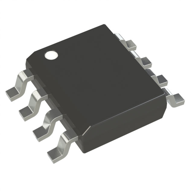
Pin Configuration and Interface Details for AT24C01C-SSHM-T
The AT24C01C-SSHM-T's pinout, based on an 8-lead SOIC footprint, facilitates high-density integration within digital architectures that rely on I²C for nonvolatile memory access. The address pins (A0, A1, A2) enable dynamic device selection, allowing up to eight EEPROMs to coexist on a single I²C bus without conflict. Their internal pull-downs simplify idle state management, yet deterministic system behavior under noise demands that each address input be explicitly driven—either to logic high or low—especially in environments with variable load or significant EMI exposure.
Interfacing mechanisms are optimized for scalability. The open-drain design of the SDA data line requires an external pull-up resistor for logic level recovery; a value not exceeding 10kΩ is recommended to strike a balance between bus speed and signal integrity. With properly calculated pull-up resistance, signal settling is maintained during clock and data transitions, preventing data corruption in multi-slave configurations. The SCL clock line mirrors these requirements but permits greater flexibility since timing margin is determined by system-level throughput and propagation delay.
Power delivery is managed through the VCC and GND pins, which should be decoupled locally with low-ESR capacitors to minimize voltage droop during write cycles. Conversely, the Write Protect (WP) input is central to safeguarding critical memory regions: it is hardware-polled at every I²C Stop condition preceding a write cycle, instantly locking the memory array when asserted. This mechanism remains immune to software faults, a crucial layer in systems requiring robust data retention under continuous power cycling or firmware reprogramming.
For packages with an exposed pad, grounding can reduce thermal impedance and improve electromagnetic compatibility. If floating is preferred for routing considerations, leakage effects are negligible due to pad isolation, although optimal performance is generally achieved when the pad shares ground potential with the main circuit plane.
In demanding scenarios—such as multiplexed sensor networks or fault-tolerant controller boards—proper pin configuration correlates directly to bus arbitration reliability. Misconfigured address or floating SDA/SCL lines are a common source of intermittent communication failures. Here, close attention to drive strength and pull-up values pays dividends; using the lower end of prescribed resistor values shortens rise times and reduces vulnerability to cross-talk.
Experience demonstrates that coupling individualized addressing with hardware write protection yields enhanced system resilience. A systematic approach—validating signal levels and provisioning fail-safe WP logic—reduces both maintenance complexity and long-term operational risk. Integrating these EEPROMs allows design teams to modularize persistent storage while maintaining global access control, especially in distributed intelligent systems. The device’s flexibility in grounding and layout further streamlines mechanical integration, supporting both single-board and stacked architectures without increasing the risk of ground bounce or data corruption.
Memory Organization and Operation Modes of the AT24C01C-SSHM-T
The AT24C01C-SSHM-T employs a straightforward yet efficient internal memory structure, partitioning its 1,024 bits into 128 words of 8 bits each. This granular organization enables precise byte-level addressing, aligning with the requirements of embedded control systems where deterministic data retrieval is essential. Device selection is facilitated through three programmable hardware address pins, expanding system scalability to accommodate up to eight unique devices on a shared I²C bus. This addressing design supports modular architectures and simplifies PCB layout, particularly in distributed sensor or configuration storage scenarios.
A closer inspection of data operation modes reveals tailored mechanisms for both flexibility and reliability. The device enables single-byte and multi-byte (page) write operations, with up to eight bytes permissible in a single write transaction—the width of one memory page. This limitation, enforced internally, precludes data wrapping into adjacent pages, which safeguards the deterministic mapping of data during high-speed sequential transactions. In practical firmware development, this constraint drives careful buffer segmentation and write logic, specifically when storing configuration tables or event logs that must maintain atomicity and logical boundaries.
Read functionality is distinguished by support for both random address reads and sequential read modes. The random read mode allows access to any specific byte, minimizing I²C traffic for sparse data access patterns. Sequential reads, conversely, are optimized for streaming larger memory segments and minimize protocol overhead. These capabilities combine to support efficient block reads for firmware or parameter updates, while also supporting targeted in-place updates with minimal bus contention.
Each transmission begins with a precise I²C start condition, followed by the 7-bit device address (including hardware-set bits), then the memory address, and finally the data bytes as per the chosen operation. Strict adherence to page boundary limits during write cycles becomes a key part of reliable driver implementation. Deviations can result in partial writes or address rollovers, leading to subtle and difficult-to-diagnose data integrity issues. Robust applications establish explicit boundary-aware write routines, sometimes exploiting the device’s predictability to maximize throughput within the allowed page window, particularly in high-frequency data logging or event capture systems.
A subtle but crucial aspect of reliable use involves timing control and state tracking. The device’s inherent write-cycle time necessitates either software polling or status flag verification before subsequent operations, especially under rapid transaction sequences. Neglecting this handshake can result in incomplete data storage—a scenario commonly mitigated by state machines or hardware-timed delays synchronized with system power management.
An often-overlooked feature is the device’s scalability for redundant or distributed memory mapping on shared buses. By leveraging all available device address combinations, data redundancy schemes or fallback parameter storage can be implemented at low complexity and cost, enhancing system fault tolerance in industrial controls and resilient sensor networks.
Integrating these mechanisms, the AT24C01C-SSHM-T delivers a balance of simplicity and control. Its predictable, page-oriented operation model suits environments where deterministic access and atomic updates are critical, while the flexible addressing scheme adapts to expanding system architectures. Employing disciplined, boundary-aware write sequences and exploiting the device’s sequential read efficiency elevates overall reliability and performance, establishing a robust foundation for both foundational and advanced nonvolatile memory applications.
Electrical Characteristics and Timing Requirements for AT24C01C-SSHM-T
The AT24C01C-SSHM-T integrates a voltage operation window spanning from 1.7V to 5.5V, accommodating interfacing with both classic 5V logic circuits and contemporary low-voltage platforms. This characteristic streamlines versatility in mixed-voltage system designs, enabling direct I/O connectivity without additional voltage-level translation components. Robust compatibility minimizes integration overhead and enhances design flexibility, particularly in intricate board layouts with multiple supply domains.
At its core, the device is engineered for rapid data exchange, supporting clock frequencies up to 1 MHz under Fast Mode Plus. This feature significantly increases throughput in memory-intensive applications where communication latency becomes a bottleneck, such as real-time data logging or firmware storage modules. High-frequency operation demands precise control of signal integrity and termination strategies, especially in compact PCB topologies; maintaining short trace lengths and proper pull-up resistor selection becomes critical at elevated I²C speeds to avoid reflections and timing violations.
The nonvolatile EEPROM leverages an internally self-timed write cycle, typically completing within 5 ms. This mechanism offloads the burden of external timing management, allowing the host to focus on transactional logic. However, dependable data retention mandates careful attention to write timing: initiating subsequent accesses before write completion can lead to data hazards. Sophisticated firmware frameworks frequently employ write-polling or acknowledge sequencing, ensuring each storage action fully commits before further traffic is attempted. Firmware should also account for cumulative write latency in multi-byte operations to preserve transactional atomicity.
A POR (Power-On Reset) circuit forms a fundamental protection layer, actively withholding functional operation until the supply voltage stabilizes above the defined minimum threshold. This preemptive reset avoids unpredictable memory access or simultaneous bus contention during system startup, which commonly occurs if power rails fluctuate or ramp-up sequences exhibit excessive slew rates. Empirical results show that adhering to VCC slew rates no faster than 0.1V/μs yields optimum stability, preventing inadvertent mode entry or errant writes in harsh environmental conditions. Careful sequencing of power-domain activations, often coordinated via PMICs or delayed enable signals, further reinforces startup reliability in multi-chip assemblies.
Electrical protection is notably robust, with input capacitance optimized to dampen transient spikes and ESD resilience exceeding 4,000V. This safeguards the device against accidental discharges during handling and mitigates susceptibility to environmental EMI, which frequently arises in industrial control interfaces or field-deployed sensor networks. When designing the physical interface, incorporating guard traces or ground planes adjacent to signal lines diminishes the likelihood of parasitic coupling, while adhering to recommended PCB layout guidelines amplifies overall immunity.
Timing requirements extend beyond initial power-up: the host must reserve sufficient delays before dispatching commands, factoring in both the minimum stabilization periods and write-cycle durations. Well-architected systems utilize hardware timers or synchronization flags, leveraging predictable startup behavior and programming sequences to maintain communication integrity. The interplay between electrical, timing, and firmware strategies forms the backbone of reliable memory subsystem operation, an insight frequently echoed in high-availability embedded applications.
Notably, the convergence of high-voltage tolerance, flexible logic interfaces, accelerated data rates, self-managed timing, and fortified protection mechanisms positions the AT24C01C-SSHM-T as a foundational element in complex control architectures. These traits collectively streamline prototyping and production, reducing the likelihood of field returns or in-situ troubleshooting, underscoring the value of integrating electrically steadfast and timing-predictable nonvolatile memory within advanced system designs.
Write/Read Operations and Data Protection in AT24C01C-SSHM-T
Write and read operations within the AT24C01C-SSHM-T utilize a well-defined I²C protocol architecture, supporting both single-byte and 8-byte page writes. The protocol mandates device addressing and sequential data transmission governed by start and stop conditions, clock synchronization, and bidirectional acknowledgment signals. These mechanisms reinforce data integrity and enable contention-free communication across multi-device buses, critical in complex embedded system deployments with multiple EEPROM instances.
Acknowledge polling is purposefully implemented to minimize wait cycles following write operations. After initiating a write, the device enters an internally timed programming cycle during which it will not acknowledge I²C commands. Polling the device for acknowledgment enables the controlling host to resume operation at the earliest possible point, optimizing throughput especially when managing high-frequency write bursts. In high-reliability applications, such as real-time data logging or configuration management, this feature streamlines firmware efficiency and aligns with deterministic scheduling requirements.
Read operations in the AT24C01C-SSHM-T are equally versatile, encompassing random read, current address read, and sequential read modes. Random read facilitates direct access to any memory byte via explicit address specification, ensuring immediate retrieval for targeted queries. Current address read benefits iterative access, automatically tracking the last read location to streamline consecutive operations, while sequential read empowers efficient bulk transfers by auto-incrementing addresses with each subsequent byte. This spectrum of read modes accommodates a range of application patterns, from single-parameter retrieval to comprehensive NVRAM extraction, and excels within boot code authentication, parameter recall, and event storage implementations.
Data protection is primarily enforced via the hardware Write Protect (WP) pin. When asserted high, the AT24C01C-SSHM-T blocks all write attempts to the entire EEPROM array, acting as a defense layer against spurious or malicious modifications. The design parses the WP status only at the onset of a write sequence—this temporal gating avoids mid-operation re-interpretation, eliminating ambiguity in write cycle outcomes. Such a mechanism is vital for systems requiring immutable regions during certain operation phases, for instance, locking critical configuration blocks after initial provisioning or when operating under escalation of privilege triggers. Floating or grounding WP re-enables writes, allowing controlled update cycles when required by the application’s operational policy.
A nuanced insight emerges from the specific timing and scope of the WP evaluation. The device's approach prevents partial writes caused by asynchronous WP assertion, ensuring that atomicity of memory programming is maintained. This characteristic aligns with robust fail-safety in fielded systems, where unpredictable events—such as electrical transients or system resets—could otherwise induce inconsistencies if write protection were re-evaluated mid-cycle. In practice, integrating WP management with microcontroller GPIO abstraction allows dynamic but reliable switching between protected and writable states, offering designers runtime flexibility while maintaining data assurance.
Adoption of these features in real-world engineering practice often involves cross-verification of state via software-side shadow copies, careful sequencing of write and protect instructions, and periodic integrity checks aligning with expected data retention profiles. Such multilayer approaches, when harmonized with the AT24C01C-SSHM-T's operational model, yield consistently reliable non-volatile storage platforms even within electrically noisy or highly secure environments.
Package Options and Physical Characteristics of the AT24C01C-SSHM-T
The AT24C01C-SSHM-T exemplifies flexibility in EEPROM design through its diverse packaging portfolio, addressing distinct requirements in both compact and conventional PCB environments. The primary configuration—the 8-lead SOIC—offers optimal balance between manufacturability and moderate board density. For heightened miniaturization, the UDFN and VFBGA packages drive footprint reduction to the sub-millimeter regime, enabling integration into space-constrained modules such as wearables and advanced sensor nodes. Conversely, PDIP and TSSOP formats provide ease of prototyping and compatibility with through-hole or high-reliability assembly. SOT23, with its streamlined outline, serves applications where board real estate and z-height are tightly constrained, such as portable consumer electronics or point-of-load regulation.
Uniform compliance with RoHS, halide-free, and green standards ensures seamless adoption in global projects and meets demands for eco-friendly hardware. Packaging selection directly influences thermal management, mechanical robustness, and assembly method compatibility. For instance, SOIC and TSSOP packages typically streamline reflow soldering, reducing process complexity and enabling high-throughput manufacturing lines. In contrast, VFBGA and UDFN facilitate advanced assembly yet necessitate precise reflow profiling and yield higher electrical performance by minimizing parasitics.
Effective PCB layout is vital to ensure the electrical integrity of the AT24C01C series. Microchip’s land pattern recommendations standardize pad geometries and solder mask requirements, which not only maximize solder joint reliability but also mitigate manufacturing defects such as tombstoning or cold joints. Signal quality hinges on judicious grounding strategies and the appropriate selection of external pull-up resistors, particularly for the I²C interface. Excessive pull-up resistance can compromise timing margins and raise susceptibility to external noise sources, while undervalued resistors increase power consumption and can generate excessive rise times, particularly in high bus capacitance scenarios.
Empirical observations show that optimizing the ground return path and minimizing trace inductance around the EEPROM enhances both noise immunity and communication reliability, especially in dense mixed-signal or RF-loaded environments. Bus trace routing and decoupling should be planned with consideration for both functional layer stacking and manufacturing panelization to prevent interference and crosstalk.
In system integration, package choice must be aligned with end-use priorities—whether favoring assembly scalability, reworkability, or stringent footprint constraints. Critical evaluation of package parasitics, board stackup, and environmental requirements not only improves performance but contributes to lifecycle reliability and maintainability. The integration of these layered considerations, from fundamental electrical nuances to application-level implications, underscores the importance of holistic thinking in package and layout selection for modern non-volatile memory deployments.
Engineering Application Considerations for AT24C01C-SSHM-T
The AT24C01C-SSHM-T Serial EEPROM integrates crucial features that address both underlying system needs and practical engineering constraints in embedded applications. Its seamless support for I²C multi-device architectures enables shared bus deployment, inviting streamlined designs where different modules require individualized nonvolatile memory. Careful bus topology planning, including the correct setting of device address pins and robust signal integrity measures, ensures error-free communication even under noisy conditions typical of industrial and automotive environments.
Deep-diving into hardware resilience, the AT24C01C-SSHM-T sustains reliable operation across an extended temperature range (-40°C to +85°C) and demonstrates strong immunity to electromagnetic interference. These attributes are vital for sensor calibration data retention or factory configuration storage, as field experience increasingly highlights nonvolatile memory corruption as a critical failure point in harsh electromagnetic scenarios. Selection of shielded PCB traces, optimized ground planes, and strategic decoupling can further reinforce memory transaction reliability.
Energy efficiency is maximized through ultra-low standby and active current characteristics, which enable continuous retention of system parameters or serial numbers without substantive impact on overall power budgets. In battery-powered deployments such as portable calibration devices, strategic use of synchronous write cycles combined with acknowledge polling reduces unnecessary idle time, accelerating transaction completion and enhancing the user sense of responsiveness. Immediate polling after writes not only minimizes latency but also prevents premature memory access, a common pitfall that undermines system integrity in fast-paced automation loops.
Pin-level considerations directly influence long-term reliability. Selection of pull-up resistors tailored to the system’s timing requirements maintains I²C signal fidelity and supports multi-node responsiveness. Unused address and write-protect pins should be managed actively—grounded or tied to known logic states—to avert random writes or spurious device enumeration. Power sequencing, if implemented with careful synchronization, eliminates the risk of inadvertent data corruption during brownout or transient conditions. Laboratory results routinely demonstrate that improper startup can lead to phantom writes, underscoring the necessity of voltage supervisors or soft-start logic in mission-critical environments.
Taken together, these layered implementation techniques distinguish robust memory integration from simple component selection. Real-world deployments benefit from a holistic approach that unifies mechanical layout, electrical discipline, and firmware strategy. With rigorous attention to design subtleties, the AT24C01C-SSHM-T supports scalable architectures and delivers predictable, long-term data retention in demanding engineering domains.
Potential Equivalent/Replacement Models for AT24C01C-SSHM-T
Selecting equivalent or replacement models for the AT24C01C-SSHM-T necessitates a thorough assessment of interface compatibility, electrical characteristics, and functional attributes that extend beyond basic datasheet alignment. At the protocol level, strict adherence to the I²C bus standard is foundational; thorough review of timing diagrams, bus voltage ranges, and I/O leakage currents under varying load conditions is essential, particularly in designs sensitive to margin or noise. Actual field-deployed systems often surface subtle timing deviations or marginal pull-up selections that can impact inter-device communication, underscoring the importance of validating alternative EEPROMs under application-specific waveforms rather than relying solely on nominal parameters.
Pinout and footprint must be verified against the application's PCB layout. Manufacturers adhere to JEDEC standards, but subtle variations in package dimensions or solder pad tolerances can complicate reflow assembly or automated optical inspection. Package marking formats and ordering information should be compared to avoid procurement of non-compliant variants or inadvertent configuration mismatches, which are frequently revealed during late manufacturing stages if unchecked.
Functionally, memory density is a primary selection criterion. The AT24C02C, a Microchip solution with an increased 2 Kbit capacity and similar pin assignment, is frequently adopted in legacy upgrades aiming for expanded address space without board revision. However, increased density may be accompanied by changed addressing schemes or block organization, requiring firmware updates, particularly if page-write operations are implemented. Direct replacements from other vendors such as ON Semiconductor’s CAT24C01 or STMicroelectronics’ M24C01 exhibit high fidelity in the 1 Kbit class, but designers must reconcile discrepancies in write endurance, data retention, and maximum write cycle duration. These parameters can prove pivotal in applications with frequent random writes or where startup integrity post power-cycling is critical.
Device-specific enhancements—such as hardware/software write protection, configurable slave addressing, or support for extended industrial temperature ranges—can impact suitability in metrology, automotive, or industrial automation use cases. Engineers should scrutinize manufacturer-provided errata and customer advisory notes; rare edge conditions such as bus arbitration anomalies or unintentional write sequencing can arise, especially in environments with mixed silicon sources or unconventional power management.
Implementing an alternate EEPROM typically involves bench-level validation, coupled with in-circuit firmware diagnostics to verify seamless memory access, data preservation across cycles, and compatibility with existing bootloaders or peripheral libraries. Such systemic validation, including compliance under diverse transient and voltage scenarios, builds real-world confidence beyond what simulation or schematic review alone affords.
Careful evaluation of the total part supply ecosystem is warranted; shifting to a replacement model sourced from a robust multi-vendor supply chain can fortify long-term availability and mitigate the risk of unplanned obsolescence, especially relevant for products deployed in embedded and safety-critical environments. Strategic selection involves not only technical matching, but also anticipation of life cycle transitions and vendor support continuity, elements that influence both short-term deployment and field-maintainability over the product’s operational lifespan.
Conclusion
Microchip’s AT24C01C-SSHM-T characterizes an advanced EEPROM solution, distinguished by its reliability and infrastructural adaptability within modern embedded systems. At its core, this device exploits proven floating-gate technology, providing stable data retention even under fluctuating voltage or thermal conditions—a critical asset for designs inhabiting challenging or unpredictable environments. Its supply voltage range from 1.7V to 5.5V ensures robust performance, accommodating devices powered through primary cell chemistries or complex multi-rail architectures.
The integration capability is further enhanced by explicit I²C bus compliance, broadening interoperability across legacy MCUs and emerging processors without demanding protocol adaptation. Engineers regularly leverage the byte-level and page-level write operations to optimize for speed or minimal power consumption, effectively matching diverse throughput requirements while minimizing application-level firmware complexity. The low active and standby current profiles are measured assets during energy-critical operations, enabling the development of battery-powered modules with extended maintenance intervals.
Data protection mechanisms play a pivotal role, with the AT24C01C-SSHM-T incorporating hardware and software write protection schemes. This dual approach mitigates inadvertent overwriting—an advantage in calibration memory, authentication key storage, or configuration parameter retention scenarios. The comprehensive package offerings—spanning compact footprints such as SOT-23 to industry-standard SOIC—simplify parallel design targeting, reducing redesign cycles when project constraints evolve between prototypes and production.
Real-world integration reveals the device’s seamless compatibility with both open-drain bus architectures and clock-stretching sequences, which expedites plug-and-play transitions in multi-vendor assemblies. During system validation, dependencies on supply sequencing or sudden environmental changes are curbed by the chip’s wide margin of operation—a feature rarely matched in equivalent parts with more stringent limits. This flexibility directly supports next-generation applications such as smart sensor nodes, automotive ECUs, and secure peripherals, where configurability, reliability, and energy constraints converge.
Drawing from these characteristics, it becomes evident that the AT24C01C-SSHM-T embodies best practices in serial EEPROM deployment by centering power efficiency, interface universality, and robust nonvolatile storage in a single, scalable platform. This engineering-centric focus allows development teams to sidestep recurring tradeoffs between legacy compatibility, energy profile, and data safety, thereby accelerating reliable bring-up across an extended spectrum of embedded solutions.