 >
>


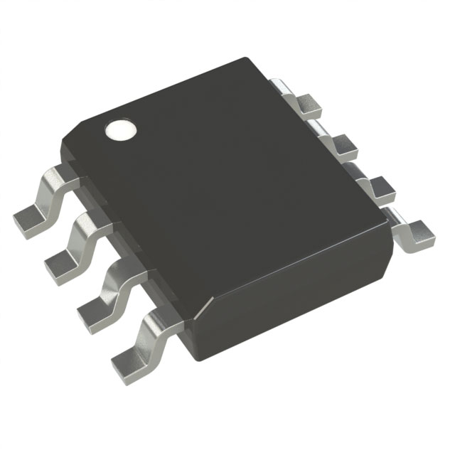
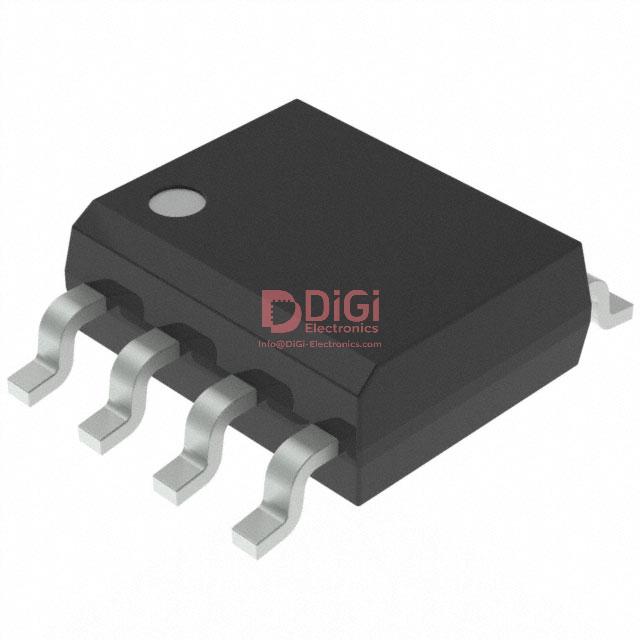
Product overview of the AT24C01C-SSHM-B Serial EEPROM
The AT24C01C-SSHM-B embodies a streamlined approach to nonvolatile serial memory integration, delivering 1Kbit electrically erasable programmable read-only memory (EEPROM) in a compact SOIC-8 package. Central to its architecture is a robust I²C-compatible interface, engineered for efficient two-wire communication. This interface supports standard (100 kHz) and fast-mode (400 kHz) I²C speeds, reducing firmware complexity while ensuring compatibility with a wide range of microcontrollers and embedded controllers. Utilizing a simple addressing scheme and supporting byte- and page-level write operations, the device optimizes both random and sequential access patterns, a critical requirement in contemporary embedded systems where both configuration data and small log storage must coexist securely.
The memory cell design leverages floating-gate MOS technology, providing intrinsic data retention exceeding 100 years and an endurance rating of 1,000,000 write cycles per byte. This engineering ensures long operational life even under frequent update scenarios, significant in parameter storage for industrial control modules, sensor configuration memory, or small-scale data logging systems. The wide operating voltage range (1.7V to 5.5V) facilitates seamless power supply integration, allowing direct coupling with logic operating at various voltage domains. This broad compatibility brings design headroom and eases power sequencing in systems transitioning between different supply rails.
In practice, the AT24C01C-SSHM-B's reliability profile extends to robust ESD tolerance and latch-up immunity, key factors in harsh electrical environments typical of factory automation, telecom infrastructure, and ruggedized portable instrumentation. The SOIC-8 form factor enables straightforward PCB layout, readily fitting into dense board designs and simplifying manufacturability for automated assembly lines.
Deploying this EEPROM addresses several common constraints in embedded systems: persistent parameter retention during power cycling, cost-efficient storage for calibration constants, and flexible recoverability from corrupted flash. Its low standby and active current draw minimize overall energy consumption, crucial in battery-powered nodes or always-on applications. The implicit insight here is the vital role of small-capacity serial EEPROMs in bridging the gap between volatile RAM and large-scale nonvolatile storage; their endurance and compatibility characteristics mitigate maintenance burdens and enable resilient configuration architectures, particularly where external flash or SD card solutions are over-provisioned or cost-ineffective.
Ultimately, the AT24C01C-SSHM-B stands out as a strategic component in the engineer’s toolkit. It harmonizes reliability, ease of integration, and operational versatility—core attributes for robust embedded platforms seeking dependable and efficiently managed nonvolatile memory resources.
Key features of the AT24C01C-SSHM-B Serial EEPROM
The AT24C01C-SSHM-B Serial EEPROM demonstrates a robust integration of advanced memory technology optimized for embedded systems, particularly where power consumption, communication flexibility, and reliability are paramount. Operating with a supply voltage as low as 1.7V, it supports a broad spectrum of power-sensitive applications and aligns with the evolving trend toward lower system voltages in modern designs.
The device’s compatibility with standard-mode (100kHz), fast-mode (400kHz), and Fast Mode Plus (FM+, up to 1MHz) I²C protocols provides engineers with the ability to tune data throughput to match system requirements. This multi-speed I²C support simplifies interfacing across diverse controller architectures, especially in systems where multiple peripheral speeds coexist. The inclusion of Schmitt Trigger inputs, coupled with on-chip noise filters, mitigates signal distortion and rejects transient glitches. Such measures safeguard data integrity on shared bus lines, a frequent pain point in densely routed PCB designs or electrically noisy environments.
Energy efficiency is engineered at both active and quiescent levels. The EEPROM consistently maintains active current below 3mA and drops standby current to 6μA, an order of magnitude improvement over legacy architectures. Practical experience shows this parameter directly extends operational lifetimes and reduces thermal footprints in battery-powered applications such as smart metering, portable medical devices, and compact sensor modules. The ability to enter extremely low-power standby without complex software handshaking streamlines system-level power management strategies.
Data security is addressed by a hardware-controlled write-protect pin, enabling global memory array protection with a single logic state. This straightforward safeguard circumvents the complexity and latency inherent in software-based protection schemes, preventing inadvertent or malicious writing during sensitive operational phases like system initialization or in-field updates. The high endurance rating of 1,000,000 write cycles per byte and guaranteed 100-year data retention ensure data persistence across extended product lifecycles, making the device particularly suited for deeply embedded, mission-critical systems that interface infrequently but must remain dependable over decades.
Reliability is reinforced through ESD protection exceeding 4,000V, effectively shielding circuitry during handling, assembly, or operation in harsh environments. The RoHS-compliant packaging promotes environmental stewardship while facilitating global supply chain acceptance.
Observations in real-world deployments indicate the combination of low-voltage operation, robust noise immunity, and reliable write protection sharply reduces system failures attributed to memory corruption or accidental overwrites. These features collectively enable streamlined hardware design by minimizing the necessity for external protection circuits or power conditioning components.
A nuanced insight emerges at the intersection of endurance, retention, and communication flexibility: The AT24C01C-SSHM-B serves as a versatile bridge between evolving platform demands and the rigid expectations of longevity, making it a strategic choice where design margins are tight, and reliability can neither be assumed nor compromised. This device exemplifies a balanced approach, advancing memory component utility well beyond traditional nonvolatile storage roles into an active enabler of resilient embedded system architectures.
Pin configuration and device architecture of the AT24C01C-SSHM-B Serial EEPROM
A comprehensive grasp of the AT24C01C-SSHM-B Serial EEPROM’s pin configuration establishes the foundation for robust system integration and reliable data storage solutions. The device arranges its primary interface around six accessible pins: three address inputs (A0, A1, A2), a write-protect input (WP), and the I²C bus interface lines, serial data (SDA) and serial clock (SCL). The address inputs enable seamless expansion, supporting up to eight devices on a single I²C bus by binary encoding their states. This design choice enables resource-efficient memory scaling in embedded systems, such as distributed sensor nodes or control modules, without additional bus lines.
The WP pin introduces a deterministic hardware safeguard, inhibiting write access to memory when asserted. This becomes crucial in safety-oriented or configuration-critical scenarios, for instance, preserving firmware parameters against inadvertent field updates. Although address and WP pins are internally pulled low, it is engineering best practice to hardwire them to explicit logic levels instead of relying on internal bias, thereby eliminating susceptibility to induced noise or undefined logic states. This is particularly important on high-density PCBs or when devices are exposed to transients commonly encountered near power electronics.
On the physical layer, the I²C SDA pin exemplifies a quintessential open-drain topology, mandating a discrete pull-up resistor (nominally ≤10kΩ) to Vcc to guarantee swift and noise-robust logic level transitions. Selection of the pull-up value represents a trade-off between bus rise time and power consumption: lower resistance yields faster response but higher quiescent draw, an essential consideration during low-power design reviews or when scaling bus capacitance due to increased device count. In practice, a 4.7kΩ resistor achieves optimal compatibility across common I²C speeds and trace topologies.
The SCL clock may be actively driven or, in multi-master systems, also benefit from a pull-up. Ensuring matched impedance and disciplined trace routing on the SCL and SDA lines further mitigates crosstalk and electromagnetic susceptibility, which is vital in applications such as automotive or industrial automation exposed to high levels of electrical noise.
Internally, the AT24C01C-SSHM-B leverages advanced signal filtering and glitch suppression circuitry—a meaningful advantage, particularly when compared against legacy parts. This fortifies signal integrity during transients such as contact bounce, ESD events, or rapid switching environments. Integrating such noise immunity features at the silicon level shifts some burden away from external circuitry and PCB layout constraints, enabling a robust design envelope even under marginal or unpredictable system conditions.
These architectural details collectively shape a device that supports not only ease of hardware addressability and secure data management, but also promotes electrical resilience crucial for production-level designs. Awareness of subtle implementation aspects, such as deliberate pin assignment and bus resistor sizing, leads directly to improved reliability and long-term data retention in real-world deployments, reflecting a strategic balance between device-level capability and system-level robustness.
Electrical specifications and performance of the AT24C01C-SSHM-B Serial EEPROM
The AT24C01C-SSHM-B Serial EEPROM exemplifies robust electrical specification management tailored for demanding embedded environments. Its operational envelope spans −40°C to +85°C, maintaining stable performance across extended temperature extremes, a feature crucial for industrial and automotive deployments where ambient conditions fluctuate considerably. The support for multiple I²C speed modes—including Fast Mode Plus (FM+) up to 1MHz—directly enables high-throughput communication without sacrificing protocol compliance, especially beneficial in systems that prioritize rapid data exchanges or host multiple memory devices on a single bus.
At system power-up, the integrated power-on reset circuitry precisely governs initialization. Internal voltage detection logic prevents inadvertent access below a defined supply threshold, thereby minimizing risk of data corruption during brownouts or noisy power transitions. Empirical experience underscores the importance of monotonic Vcc ramping; erratic or undershooting supplies can disrupt memory cell integrity, especially in highly miniaturized boards where voltage overshoot or undershoot occurs due to parasitic elements. Designers routinely implement controlled sequencing in power distribution networks to align with the device’s requirements, contributing to reliable in-field operation.
Electrical design margins rest on strict adherence to the EEPROM’s absolute maximum voltage and current ratings. Surpassing these limits, whether during transient events or steady-state operation, poses a threat to both the memory array and peripheral I/O circuits. Iterative hardware validation cycles frequently include margin-testing for supply and I²C pull-up values to ensure safe operation under worst-case conditions. This approach mitigates latent failure modes and bolsters long-term system reliability benchmarks.
Central to write functionality is a self-timed, internally managed process. Typical write cycles execute within 5ms, with the device autonomously disabling further write commands until completion. This barrier is fundamental for preserving data consistency, precluding bus contention scenarios where premature accesses might induce bit errors or page faults. Insights from mixed-speed bus implementations highlight the necessity for precise timing analysis, especially when write cycle acknowledgement interacts with host-side microcontroller firmware. Proactive polling and interrupt strategies are often employed in firmware to efficiently coordinate with EEPROM busy states, improving both throughput and predictability in data logging or configuration management applications.
High-speed operation and multi-node bus topologies demand deliberate attention to bus capacitance and timing budgets. Excessive capacitance, whether from trace length or aggregate device input, can degrade signal integrity and reduce timing margins below specification, manifesting as communication errors particularly at FM+ rates. Engineering best practices advise partitioning device placement and leveraging lower voltage swings, complemented by rigorous signal integrity modeling and routine impedance measurements during prototyping. This methodology proves effective in maintaining reliable clock/data waveforms across extended PCB layouts, supporting complex platform scalability.
Layering these technical foundations reveals that the AT24C01C-SSHM-B offers dependable and scalable non-volatile memory integration for systems requiring both performance and robustness. Its architecture and operation are tightly aligned with the demands of modern electronic design, with nuanced engineering strategies enabling deployment in sophisticated application scenarios ranging from industrial instrumentation and automotive networking to consumer devices where reliability and throughput are paramount. Carefully harmonizing power, timing, and signal characteristics in real-world environments demonstrates that nuanced engineering decisions are pivotal to unlocking the full potential of this serial EEPROM.
Operational modes and communication protocol of the AT24C01C-SSHM-B Serial EEPROM
The AT24C01C-SSHM-B Serial EEPROM operates as a dedicated I²C bus peripheral, leveraging a two-wire communication interface engineered for both simplicity and robustness. Its protocol adheres to an I²C-compliant signaling framework, where each interaction initiates with a distinct start condition and closes with a stop condition, encapsulating data frames for orderly exchanges. Data transfer occurs with the Most Significant Bit (MSB) transmitted first across 8-bit segments, and each byte is immediately acknowledged through the acknowledge/nacknowledge handshaking mechanism, providing a foundational integrity check and minimizing undetected line errors.
Within the I²C structure, the AT24C01C-SSHM-B assumes a passive, responsive posture as a bus slave, only reacting to address and command sequences issued by the active master. Clock and data lines (SCL and SDA) are governed by precise timing constraints; the device’s inbuilt spike suppression circuitry filters hazardous transients, addressing the vulnerability of serial buses to radio frequency interference and sharp voltage dips. This enables integration in environments where moderate EM noise is present or multiple buses contend for signal clarity.
A pivotal aspect of the device’s operational suite is its low-power standby mode, which is automatically entered when inactive between communication events, minimizing system power draw without explicit external intervention. For error correction and resiliency, the AT24C01C-SSHM-B enables a protocol-level software reset mechanism. This sequence does not demand power cycling the device and allows the bus to recover gracefully following errant signal collisions or aborted transfers. Such a feature preempts frequent field failure modes, streamlining fault recovery in complex embedded networks.
System architecture utilizing the AT24C01C-SSHM-B benefits from these mechanisms in typical scenarios such as microcontroller-based configurations, remote sensor endpoints, and programmable configuration storage. Reliable communication, facilitated by the strict acknowledgment scheme and the noise-immunity measures, reduces the need for extensive retry or recovery code. Moreover, the seamless transition into standby mode extends device lifetime where power efficiency is prioritized, such as in battery-operated systems or dense modular assemblies.
Engineering experience frequently reveals that failure to rigorously implement timing and acknowledgment processes results in bus deadlocks or stale reads in multi-device, multi-master frameworks. Implementers who exploit the device’s protocol-driven recovery pathways and adhere to its precise timing recommendations achieve higher communication stability and avoid low-level issues like ghost addressing or inadvertent writes during bus transients.
The device’s architecture reflects a fundamental design insight: optimizing nonvolatile memory access not only through the underlying silicon process, but by embedding operational resilience and error handling at the protocol level. This approach shifts reliability upward in the stack, benefiting the application layer and supporting versatile deployment across diverse, noise-prone embedded topologies. Advanced bus management and self-healing attributes highlight the AT24C01C-SSHM-B as a model peripheral for robust and scalable I²C ecosystems.
Memory organization and addressing in the AT24C01C-SSHM-B Serial EEPROM
Memory organization in the AT24C01C-SSHM-B Serial EEPROM is defined by a compact structure: 128 individually addressable bytes arranged within 16 pages, each page comprising 8 bytes. This breakdown facilitates both granular byte-level read/write and efficient page-level operations, optimizing data throughput and minimizing write cycle overhead where sequential data must be stored or retrieved. The design leverages an 8-bit addressing protocol. The upper three bits (A2, A1, A0), embedded within the device address byte, enable hardware-level device multiplexing—essential for scalable, multi-device I2C topologies. By tying these pins to distinct logic levels across devices, concurrent access and device identification are streamlined, supporting robust multi-chip implementations within a shared bus environment.
Addressing within the chip employs a word-address byte, where the most significant bit is a “don’t care” for the AT24C01C, effectively narrowing the internal addressable range to seven bits (0–127). This detail must be tightly integrated into firmware logic to avoid erroneous addressing, as overlooking the ignored bit can propagate subtle bugs during data access. The byte and page-oriented scheme directly influences optimal application-layer memory mapping. Sequential writes that align with page boundaries maximize EEPROM lifespan by reducing unnecessary overwrite cycles, while random single-byte changes offer flexibility for configuration storage, error logs, or user settings. However, awareness of the page write buffer’s capacity (8 bytes) is critical. Writing more than a page’s worth in a single sequence will wrap data within that page, potentially overwriting existing data—a key consideration when designing storage protocols for parameter tables or streaming logs.
On the physical design level, packaging impacts address configuration—specifically in space-constrained footprints like SOT23. Here, absence of break-out pins for A0, A1, and A2 means device address defaults to all logic ‘0’. This restriction enforces singular-device occupancy per bus segment for such packages unless supplemented by port expanders or bus switches. Engineers integrating these variants must account for board-level isolation, signal integrity, and system scalability if more EEPROM devices are anticipated.
Experienced practice reveals that PCB layout strategies should incorporate robust pull-up provision for the I2C lines and prior simulation of cross-board capacitance. This precludes bus contention and mitigates communication errors when scaling beyond a handful of devices. Additionally, for multi-device scenarios, thoughtfully allocated address lines reduce debugging complexity and bus scanning time. Low-level interface drivers benefit from conditional masking of the “don’t care” address bits within software routines, forestalling peripheral anomalies during batch command operations.
A core architectural insight is that the AT24C01C’s addressing model, by virtue of hardware address multiplexing and structured memory paging, underpins both scalability and reliability. Applications can exploit nonvolatile logging, hierarchical data caching, and rapid configuration reloads with predictable endurance, provided the memory-map design respects page-alignment and addressing boundaries. Future designs may further enhance resilience by interleaving devices at different logical addresses, distributing high-write tasks and extending total duty cycle. So, careful synthesis of hardware topology, memory management logic, and device-level address control remains pivotal in harnessing the full potential of the AT24C01C-SSHM-B’s architecture.
Write operation techniques in the AT24C01C-SSHM-B Serial EEPROM
Write operation techniques in the AT24C01C-SSHM-B Serial EEPROM hinge on robust command sequencing and attention to memory architecture. The device facilitates single-byte writes for addressing individual memory cells and page-write operations for more efficient bulk programming. In page-write mode, up to 8 contiguous bytes within a single page buffer are loaded prior to the internal write cycle—a design that mitigates I2C bus overhead during sequential data updates. The internal address pointer automatically increments after each byte, but it does not cross the defined page boundary. Ensuring that write sequences do not extend beyond a page limit is critical; if the internal counter overflows, subsequent bytes overwrite data at the beginning of the current page, potentially introducing functional anomalies, especially in settings where atomic configuration storage matters.
The underlying write protocol employs acknowledge polling to maximize throughput in time-sensitive use cases. After dispatching a write command, the microcontroller can issue repeated slave address calls with the write bit cleared, proceeding only when an acknowledge is returned by the EEPROM. This handshake mechanism obviates the need for conservative fixed-delay loops, streamlining firmware event handling and enabling tighter main loop scheduling in real-world systems.
The WP (Write Protect) pin architecture provides another layer of fail-safe assurance. Driving WP high (to Vcc) masks all write attempts, preserving data integrity; this measure is indispensable in applications requiring persistent, tamper-resistant parameter storage or during system firmware upgrades where accidental EEPROM updates could cause unrecoverable states. Conversely, asserting WP low enables authorized overwrites, affording flexibility during production calibration.
Structuring EEPROM writes with these constraints mandates that system designers tightly manage both addressing and write enable logic. For instance, in practice, when programming configuration arrays spanning multiple pages, the firmware must partition data and align page boundaries, invoking discrete write cycles to prevent inadvertent rollback. Efficient polling routines, integrated into interrupt-driven I2C stacks, can leverage minimal CPU cycles to detect write completion.
Recognizing that endurance and data retention are direct functions of write energy management, firmware strategies often sequence bulk updates via page-write—minimizing per-byte wear and leveraging the shorter cumulative write latency. This architectural awareness, coupled with proactive WP management and the use of acknowledge polling for synchronization, delivers both reliability and efficiency for systems using the AT24C01C-SSHM-B. Integrating these sophisticated techniques into control flows not only prevents data integrity risks but also optimizes overall I2C bus utilization, benefiting applications ranging from secure credential storage to adaptive configuration in complex embedded architectures.
Read operation options in the AT24C01C-SSHM-B Serial EEPROM
Read operation options in the AT24C01C-SSHM-B Serial EEPROM are streamlined to address various use scenarios through three distinct modes: current address read, random address read, and sequential read. Each mode is underpinned by the manipulation of the device’s internal address pointer, a fundamental component managed via the I²C command structure.
The current address read mode leverages the internal address pointer's state, retrieving the byte at its present address without specifying a new target location. This is optimal when executing multiple consecutive reads, particularly in loop-driven buffer management, as the address pointer remains synchronized with prior operations. This mode minimizes bus traffic since there is no address redefinition overhead, contributing to improved throughput in tightly coupled polling loops or real-time monitoring routines.
Random address read introduces flexible access to any nonsequential memory location. It employs a "dummy write" operation—initiating an I²C write sequence to set the desired address pointer without the final data phase—then immediately switches to a read command. This mechanism decouples data access from sequence continuity, enabling rapid retrieval of configuration bytes, calibration data, or event logs stored at arbitrary locations. Robust system designs implement this mode when deterministic address targeting outweighs continuous block access, such as accessing command registers interleaved within larger data structures.
Sequential read mode automates block data extraction by leveraging the pointer’s auto-increment feature. Upon each successful read, the EEPROM advances the pointer, allowing uninterrupted retrieval of consecutive bytes up to the storage boundary. This method suits applications like memory dumps, data streaming, or batch sensor data logging, where high-speed access to long records is required. The inherent auto-roll-over at the EEPROM boundary, however, mandates buffer management mechanisms to prevent over-reading and potential data misalignment. Overlooking this detail in firmware design can generate subtle memory wrapping bugs, particularly when the dataset size approaches the physical storage limit.
Practical deployment frequently involves combining these read modes for efficiency. For instance, initialization routines may launch with targeted random reads for device identification and calibration values, then transition to sequential reads for bulk data transfer, and finally revert to current address reads in performance-critical polling cycles.
An implicit insight is the importance of aligning read operations with the underlying bus topology and application-level latency requirements. Optimal throughput arises from minimizing address pointer updates except when true random data access is required. Furthermore, effective error handling around the dummy write phase in random address reads mitigates bus contention issues, ensuring device integrity across complex I²C networks.
For engineering teams, the nuanced selection among these read mechanisms directly impacts system responsiveness, code complexity, and data integrity. Structured layering of read modes, mapped to specific workflow phases, yields scalable and maintainable memory access strategies, especially as EEPROM density and data acquisition frequencies increase in embedded solutions.
Packaging and physical considerations for the AT24C01C-SSHM-B Serial EEPROM
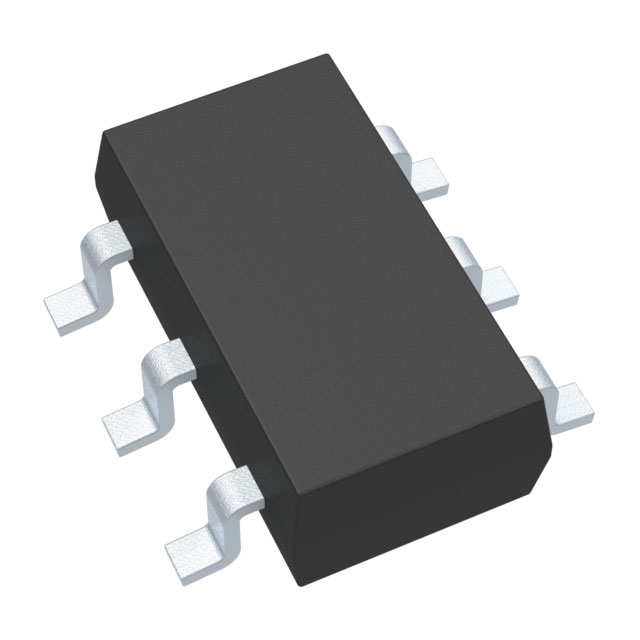
Packaging options for the AT24C01C-SSHM-B Serial EEPROM span multiple industry-standard formats, optimized to address diverse integration and manufacturing requirements. The 8-lead SOIC, specifically denoted under the -SSHM-B suffix, serves as a balance between footprint efficiency and handling ease, facilitating streamlined surface mount assembly. Other available variants, including PDIP, TSSOP, UDFN, SOT23, and VFBGA, extend practical choices for applications constrained by physical space, automated pick-and-place limitations, or high-density board architectures.
Mechanically, each package type adheres to Microchip’s comprehensive dimension tables and recommended PCB footprint configurations. These ensure precise alignment with automated soldering and inspection tools, supporting consistent yield across variable production scales. The pin marking guidelines—contrasting chamfered corners or laser-etched labels—are standardized for clear visual identification, minimizing the risk of orientation errors during component placement.
All provided packages fulfill RoHS compliance, integrating lead-free construction and compatible materials for aggressive thermal profiles. During reflow soldering, thermal mass and exposed pad geometry influence heat absorption and joint integrity; engineers routinely verify preheat ramp rates and peak dwell times, especially for ultra-small bodies such as VFBGA or UDFN, mitigating potential issues like tombstoning or void formation.
Selecting an optimal package demands technical judgment across several parameters: available PCB real estate, compatibility with existing assembly equipment (notably nozzle types and vision systems), and ambient operating conditions. For instance, PDIP packages simplify prototyping and manual handling but may not suit compact systems where TSSOP or SOT23 footprints are preferable. In automated high-throughput manufacturing, lead pitch and coplanarity specifications directly affect placement yields, prompting careful validation against target design rules.
A nuanced approach accounts for both electrical performance and mechanical reliability under operational stress. Smaller packages, while enabling higher board density, may pose increased risk from thermal cycling or mechanical shock, especially in industrial or automotive deployments. Conversely, larger bodies support enhanced solder joint strength but can constrain layout flexibility. Experience shows that early consultation with assembly partners and iterative footprint simulations help preempt unexpected process or reliability concerns.
Ultimately, package selection for the AT24C01C-SSHM-B influences downstream design, manufacturing, and lifetime reliability. Integration strategies benefit from balancing form factor constraints with process capabilities, paying close attention to standardized landing patterns and proven assembly parameters. Deploying robust validation protocols—from X-ray inspection of solder joints to in-situ temperature cycling—ensures that the chosen configuration delivers consistent system-level performance.
Potential equivalent/replacement models for the AT24C01C-SSHM-B Serial EEPROM
Selecting an equivalent or replacement EEPROM for the AT24C01C-SSHM-B requires attention to the underlying I²C protocol standardization and electrical compatibility. The AT24C02C Series from Microchip offers a direct upgrade path, doubling nonvolatile storage to 2Kbit (organized as 256 bytes), while retaining identical supply voltage boundaries and I²C address structure for straightforward migration. In scenarios where larger page sizes, unique packaging, or tighter write endurance specifications are critical, the broader AT24CxC portfolio presents incremental scaling while holding fast on communication protocols and logic thresholds, provided the selected alternative maintains operational voltage overlap and single-supply requirements.
Consistency at the hardware interface is crucial; pin assignment and onboard address select bits must mirror those of the original AT24C01C-SSHM-B to avoid system-level rework. Engineering best practices dictate careful cross-referencing of page write limitations, bus capacitance tolerance, and quiescent current profiles, especially when shifting between devices with expanded capacity or differing process technology. Subtle differences—even within the same manufacturer’s lineup—can manifest in write cycle times or maximum allowed clock frequencies, affecting firmware timing constraints or data integrity during burst writes.
Circuit reliability depends on maintaining electrical margins across temperature, supply fluctuation, and noise immunity parameters. For instance, swapping to a part with a slightly different voltage threshold may necessitate reviewing the host microcontroller’s pull-up resistor sizing and power-up sequencing logic. Practical designs benefit from staged migration, where prototypes validate not only functional compatibility but also endurance in field-relevant stress conditions such as repeated page writes and recovery from brownouts.
Migrating to alternatives within the same device family facilitates minimal software changes if addressing and block structure rules remain untouched. However, leveraging the expanded capacity of a device like the AT24C02C unlocks opportunities for enhanced data logging or configuration storage without architectural overhaul. The layered approach, beginning with electrical and protocol parity, progressing through pinout and timing verification, and culminating in in-circuit reliability assessments, emerges as the optimal migration pathway. It is advisable to leverage direct manufacturer migration guides and cross-reference the latest datasheets against application requirements, ensuring sustained interoperability and robust memory performance in the target environment.
Conclusion
The AT24C01C-SSHM-B Serial EEPROM, designed by Microchip Technology, represents a robust solution for non-volatile memory integration within embedded systems, prioritizing data integrity and power efficiency. Centered on the I²C communication protocol, the device delivers straightforward host connectivity with minimal overhead, facilitating its adoption across a range of microcontroller architectures. Simplified bus arbitration and well-documented command sets streamline firmware development, reducing validation cycles for rapid prototyping and deployment.
Mechanically, the device provides multiple package options, easing PCB layout constraints and supporting high-density assemblies subjected to rigorous space and thermal requirements. The onboard hardware write-protection feature significantly decreases the risk of unintentional modifications to critical calibration or boot data, a frequent pain point in firmware revision processes. This write-defend mechanism directly translates to enhanced root-cause traceability and operational uptime in fielded systems, particularly where field updates or remote diagnostics are routine.
The EEPROM’s high endurance specification ensures reliable service through repeated program/erase cycles and counters typical wear-out mechanisms, thereby extending system lifetime and reducing maintenance overhead. Deep endurance, coupled with stable data retention, underpins its suitability for roles such as configuration parameter storage, runtime state retention, event history logging, and security key management. For instance, when deployed in industrial sensor modules, the AT24C01C-SSHM-B enables granular logging of environmental events and failsafe storage of compensation factors, ensuring consistent sensor accuracy across calibration intervals.
Integration within legacy designs also benefits from the EEPROM’s functional compatibility and incremental feature-set enhancements. It serves as a straightforward replacement for older serial EEPROMs, minimizing re-qualification efforts and enabling seamless upgrades without intrusive hardware modifications. In NPI (new product introduction) scenarios, its maturity and broad ecosystem support translate to ready access to reference designs and proven software stacks, streamlining time-to-market.
A strategic evaluation extends beyond current fit; memory device selection impacts long-term product viability. Incorporating the AT24C01C-SSHM-B supports modular design principles, allowing for later migration to higher capacities or pin-compatible footprints as application requirements grow or regulatory standards evolve. While newer storage technologies offer density advantages, the predictability and deterministic access patterns of I²C EEPROM continue to justify their role where simplicity, reliability, and supply longevity are paramount.
By delivering a balanced profile of performance, data integrity, and integration flexibility, the AT24C01C-SSHM-B emerges as a resilient choice for engineers targeting both contemporary and transitional platforms. Its nuanced feature mix and operational robustness position it as an enabling component in diverse and demanding embedded contexts.