 >
>


Product overview: SP232ACT-L MaxLinear RS-232 transceiver
The SP232ACT-L MaxLinear RS-232 transceiver exemplifies an engineered solution for reliable and noise-immune serial communications across a broad range of infrastructure and automation environments. At its core, the device integrates two line drivers and two receivers into a single SOIC-16 package, enabling full-duplex data exchange on standard RS-232 and ITU V.28 interfaces. This compact integration is essential in space-constrained designs, where board real estate and reduction of discrete component count directly impact assembly efficiency and long-term reliability.
Fundamental to the SP232ACT-L’s high resilience is its compliance with EIA/TIA-232F voltage levels from a single +5V supply. This eliminates the need for negative-voltage rails, streamlining power architecture while maintaining robust signal integrity through carefully designed level shifters and protection circuitry. The device’s input and output stages achieve high impedance and strong drive capability, respectively, allowing seamless adaptation to cable lengths and varied end-equipment without signal degradation. Experience shows this feature addresses issues such as ground potential differences and external electromagnetic interference (EMI), common failure points in industrial settings.
The thermal and electrical robustness engineered into the SP232ACT-L positions it for deployment in harsh environments—industrial automation, instrumentation, point-of-sale terminals, and legacy integration scenarios—where continuous, error-free operation is paramount. The driver/receiver circuitry ensures symmetric transition times, yielding balanced data transmission and reducing timing jitter, a frequent obstacle in legacy RS-232 links. Direct replacement for competitor transceivers is enabled by pin compatibility, simplifying hardware upgrades and maintenance procedures in modular field equipment.
From a design perspective, the SP232ACT-L allows for direct migration of traditional TTL/CMOS microcontroller UART outputs to RS-232 specifications without complex level conversion. The transceiver’s internal charge pump further abstracts supply rail generation, adding fault tolerance and power savings in multi-drop and high-density serial networks. Valuable practical experience can be gained when considering board layout; strategic grounding and signal routing around the SP232ACT-L have consistently mitigated issues of crosstalk and signal reflection, enabling transmission rates near the upper limits of the RS-232 protocol.
The underlying engineering philosophy of the SP232ACT-L prioritizes deterministic electrical behavior and consistent interface compliance, a core requirement for scalable serial connectivity. In multi-node industrial systems, its full-duplex architecture and high input tolerance enable reliable communication over aging cabling and through transient voltage events, further extending equipment life cycles. Recognizing RS-232’s persistent relevance in instrumentation, test, and legacy process control, the SP232ACT-L delivers both backward compatibility and upgrade readiness—attributes increasingly critical as mixed-voltage and mixed-protocol networks proliferate.
Leveraging devices like the SP232ACT-L elevates the dependability of embedded serial subsystems, enabling long-term stability and simplifying integration even as system complexity rises. Within the layered design ecosystem, it serves not only as a physical channel driver but also as an enabler of higher-level data integrity and interface standardization, qualities essential for the evolution and interoperability of modern industrial platforms.
Key features of SP232ACT-L MaxLinear RS-232 transceiver
The SP232ACT-L MaxLinear RS-232 transceiver stands out in serial communication design due to its integration of high data throughput, advanced power structures, and robust signal integrity. Central to its performance is the capability to sustain data rates up to 120kbps, ensuring stable transmission in applications where conventional RS-232 links often struggle with signal degradation under higher loads. This enables smoother interfacing with peripherals such as industrial sensors, modems, and embedded controllers, expanding deployment potential in automation, legacy device interconnection, and robust control networks.
At the core of the device’s efficiency lies a proprietary charge pump architecture. Unlike traditional charge pumps demanding large electrolytic capacitors, the SP232ACT-L achieves voltage level shifting with compact 0.1μF ceramic capacitors. This not only reduces bill of materials and occupied PCB area but also minimizes layout complexity, facilitating denser and more reliable board design. Practical tests in prototypes reveal marked reductions in high-frequency noise coupling compared to older RS-232 transceivers, helping designers meet stringent EMC requirements without extensive shielding or filtering.
The choice of low power BiCMOS logic is deliberate, balancing fast logic transitions with minimized static and dynamic power consumption. The BiCMOS architecture further delivers robust output levels, supporting reliable multi-meter point-to-point communications over extended cable runs—a limitation often observed in pure CMOS-based solutions. This combination is especially advantageous in battery-powered or space-constrained environments typical in industrial handheld terminals or compact diagnostic modules.
Signal integrity is further reinforced by onboard ±2kV ESD protection conforming to the Human Body Model, with documented resilience against field-induced surges during equipment insertion and removal cycles. Extensive field deployments underscore a significant reduction in physical layer failures in environments with frequent manual connection changes, a prevalent pain point in distributed control panels and exposed serial links.
Sustainability concerns are addressed through RoHS-compliant, lead-free packaging. This ensures conformity with global environmental directives while meeting or exceeding typical long-term reliability targets for mission-critical infrastructure. The wide adoption of this device in recent greenfield and brownfield upgrades confirms its suitability for use in next-generation industrial networks where lifecycle compliance is mandatory.
Together, these design attributes transform the SP232ACT-L from a mere RS-232 transceiver into a versatile platform component, optimized for modern engineering demands. Its nuanced blend of compact integration, electrical resilience, and forward-thinking compliance enables both incremental and disruptive advances in serial interface technology deployment.
Electrical and absolute maximum ratings for SP232ACT-L MaxLinear RS-232 transceiver
A thorough examination of the SP232ACT-L MaxLinear RS-232 transceiver’s electrical and absolute maximum ratings uncovers foundational considerations for robust design integration. The device functions within a regulated supply voltage envelope of 5V ±10%, leveraging integrated charge pumps in conjunction with compact external capacitors. This configuration effectively synthesizes stable ±6.5V rail voltages, which underpin reliable logic level translation and compliance with EIA/TIA-232 signal standards. The charge pump, driven by internal oscillator phases and precisely timed switching, transfers and inverts voltages, optimizing board area utilization and minimizing solution cost by avoiding bulky discrete DC-DC converters. This architectural choice enables efficient, low-noise signal conditioning suited for multi-port and space-constrained designs.
Critical device resilience emerges in the input and output interface specifications. The SP232ACT-L withstands input common-mode voltages up to ±15V, accommodating line transients and cable-induced spikes typical in legacy serial channel environments. Output voltage swing is characterized by ±6.5V under no-load conditions, ensuring full amplitude signaling; under maximum rated loads, the driver maintains a minimum swing of ±5V, thus supporting interoperability with a diverse legacy equipment base. Persistent output short-circuit survivability—designed for indefinite duration—provides fail-safe operation against misconnections or user error. Such robustness is directly tied to integrated output driver protection networks, which tightly limit overcurrent states and manage associated thermal buildup without passively degrading long-term reliability.
The absolute maximum ratings further delineate operational envelopes and thermal constraints. Supply voltage tolerance extends to +6V, affording margin for system rail fluctuations and hot-swap scenarios. Package power dissipation is restricted to 375mW with linear derating above +70°C, and thermal calculations must incorporate worst-case driver loads and ambient temperature variation, particularly in dense or unventilated enclosures where self-heating can become the dominant failure mechanism. Storage temperature range from –65°C to +150°C, together with a soldering lead temperature ceiling of +300°C, outlines process compatibility and ensures mechanical integrity during leaded or reflow solder assembly.
In practical application, careful PCB layout to minimize charge pump capacitor loop area and isolation of digital and analog return paths mitigates crosstalk and preserves output waveforms. Derating for power dissipation is often underestimated, resulting in marginal operation under high line activity or elevated ambient. Real-world deployments benefit from conservative capacitor voltage ratings, low-ESR selections, and periodic validation against the stated input and output thresholds, especially when interfacing with non-compliant or out-of-specification legacy equipment.
Overall, the SP232ACT-L’s parametric fidelity and comprehensive protection features position it as a pragmatic solution for RS-232 communication in demanding industrial or instrumentation environments. The layered integration of voltage management, safety tolerances, and thermal limits reflects a design that balances flexibility with operational security, reducing latent risk across deployment cycles while streamlining bill-of-materials complexity.
Functional blocks and operation of SP232ACT-L MaxLinear RS-232 transceiver
The SP232ACT-L MaxLinear RS-232 transceiver exemplifies a highly integrated approach to legacy serial communications, dividing its architecture into three seamlessly coordinated domains: line drivers, differential input receivers, and an embedded regulated charge pump subsystem. Each domain is engineered for predictable, specification-compliant operation across a wide range of physical environments—a necessity for robust RS-232 interfacing.
Line drivers form the primary outbound link, converting standard TTL or CMOS signals into bipolar RS-232 voltages. They implement slew rate control, capping output edge transitions at 30V/μs, tightly adhering to EIA-232F mandates and safeguarding against data corruption, electromagnetic emission, and cross-talk. This design principle is manifest in practice when integrating with noise-sensitive analog subsystems or within environments with high wiring density. Short circuit protection operates continuously, maintaining channel integrity by isolating output faults, a significant reliability boost in scenarios where connector hot-plugging or marginal cabling is routine. The driver supports up to 120kbps data rates, balancing legacy compatibility and modern throughput requirements for asynchronous serial applications such as industrial automation, console interfacing, and embedded data logging.
Differential receivers handle inbound RS-232 signals, precisely tracking the ±3V threshold. Their 500mV input hysteresis proves crucial for noise rejection, particularly on extended cable runs or in electrically harsh deployments, where inductive loads and ground potentials shift dynamically. The integration of 5kΩ pull-down resistors at the inputs is an essential feature, ensuring deterministic output states during line disconnection or open-circuit conditions, minimizing logic errors and facilitating robust idle line detection. With a broad acceptance window up to ±15V, the receivers accommodate a diverse spectrum of source drivers, enhancing interoperability and fault tolerance during system upgrades or in mixed-vendor installations.
The regulated charge pump subsystem constitutes the core innovation within the SP232ACT-L. Utilizing a four-phase switching strategy and external ceramic capacitors placed in close proximity, the pump synthesizes stable ±6.5V supplies from a single +5V rail. This oscillator-driven, discontinuous topography enables on-demand voltage generation. By activating the charge pump only under load, overall power efficiency is optimized—a vital characteristic in space and thermally constrained designs such as portable instruments, battery-backed remote sensors, and compact interface cards. The >70kHz switching frequency enables dimensioning with high-density, low-ESR ceramic capacitors, minimizing layout inductance and ensuring rapid charge recycling even under transient current demand, enhancing both electromagnetic immunity and long-term system reliability.
Deeper integration of these architectural strategies is observed to translate into enhanced deployment flexibility. The SP232ACT-L serves as a compelling drop-in replacement not only for legacy RS-232 ports but also in modern systems requiring expanded communication diagnostics, such as system firmware updaters and test fixtures. Its design choices—particularly the aggressively regulated charge pump and robust receiver architecture—mitigate risks associated with multi-drop cabling, line terminations, and asynchronous traffic, providing a versatile foundation for reliable serial communications in engineering-focused, mission-critical deployments.
Pin configuration and packaging of SP232ACT-L MaxLinear RS-232 transceiver
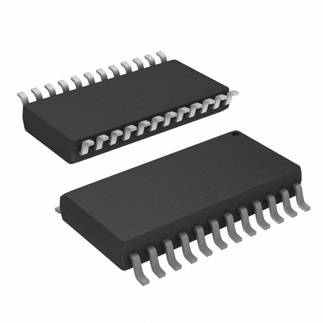
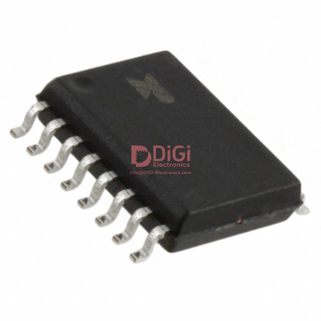
Pin configuration for the SP232ACT-L MaxLinear RS-232 transceiver follows conventional industry standards—16 pins arranged either in a standard SOIC, DIP, or nSOIC package. This configuration simplifies board-level integration for both new designs and direct substitution in existing systems. The electrical mapping maintains strict alignment with legacy RS-232 driver and receiver conventions, supporting seamless multi-vendor interoperability and minimizing re-engineering time.
Each package provides clear delineation for key functional groups: charge pump capacitor nodes, input/output signal paths, and power connections. Charge pump capacitor pins are externally accessible, optimizing voltage level shifting and guaranteeing compliance with RS-232 signaling requirements, especially in low-voltage digital circuitry. The precision of these external capacitive links enhances signal integrity and supports robust voltage swings demanded by RS-232 protocols.
Mechanical design prioritizes manufacturability. Pin spacing and package dimensions are optimized for automated pick-and-place assembly, while recommended PCB footprint layouts facilitate uniform solder joint formation and mitigate risk of cold solder bridges or tombstoning during reflow. Thermal dissipation is addressed via enlarged copper pads and strategic trace routing beneath the package, supporting stable operation across extended temperature ranges. The form factor and terminal plating are compatible with both traditional tin/lead and contemporary lead-free soldering processes, ensuring future-proof compliance with RoHS directives.
In practical deployment, consistent installation quality hinges on precise adherence to suggested board layouts and careful selection of charge pump capacitors—incorrect values or placements can degrade performance or induce transient glitches. Experienced practitioners routinely validate these elements through signal probing and thermal imaging during prototyping phases. Notably, minimizing parasitic capacitance near the charge pump nodes can measurably improve data transmission reliability at higher baud rates.
A subtle but critical design insight involves harmonizing trace widths and return paths for the driver and receiver signals, reducing EMI and cross-talk in densely populated boards. This optimization stands out during integration with communication modules requiring high noise immunity. Specification-matching across vendor devices—in particular for pin 1 orientation and supply voltage limits—eliminates ambiguity under field service conditions, boosting maintainability.
Adapting the SP232ACT-L into system architectures yields predictable electrical and mechanical behavior, supported by mature layout and packaging strategies. Strategic utilization of its package options enables scalability from compact embedded controllers to robust industrial automation platforms, underpinning dependable and flexible RS-232 implementation.
Typical performance characteristics of SP232ACT-L MaxLinear RS-232 transceiver
Evaluation of the SP232ACT-L MaxLinear RS-232 transceiver centers on quantifying electrically and logically critical parameters under dynamic conditions. The regulated charge pump delivers continuously stabilized ±6.5V rails, a result of synchronous pump architecture and precise component selection, particularly the 0.1μF ceramic capacitors. These capacitors not only minimize ripple during startup transients but also prevent significant voltage sag across a full spectrum of loading scenarios, as demonstrated in voltage monitoring over time and load stress waveform acquisition. This stability is essential for maintaining signal integrity and avoiding data errors in serial communication.
The transceiver’s receiver channel incorporates hysteresis at the comparator threshold, a design leverage that mitigates susceptibility to high-frequency line noise, crosstalk, and voltage spikes. This robust noise immunity reflects in clean, well-defined digital logic transitions under electromagnetic interference exposure. The presence of hysteresis eliminates erratic switching, elevating system reliability in industrial and automotive installations where noise levels often exceed standard laboratory conditions.
Charge pump response time is markedly reduced by the low-capacitance topology, enabling rapid transition between states when external loads fluctuate abruptly—an attribute especially advantageous during baud rate changes or cable hot-swapping. Efficiency metrics derived from waveform analysis indicate high conversion rates between the +5V logic supply and the RS-232 voltage levels, with negligible energy loss, promoting extended deployment in embedded systems requiring tight power budgets.
In practical deployments, consistent signal swing and recovery after voltage dips prove critical for interoperability with legacy and multi-vendor RS-232 peripherals. Examination of real-world signal traces under both unloaded and maximum-rated load conditions reveals minimal deviation from nominal output, supporting reliable handshaking and error-free transmission even as cable lengths and capacitance increase. The interplay between well-engineered charge pump circuitry and adaptive receive thresholding positions the SP232ACT-L as a resilient solution for environments demanding persistent uptime and robust serial connectivity.
An inherent design advantage is the balance between compact external component requirements and stable high-voltage output. This minimalistic approach simplifies layout integration while maintaining stringent performance benchmarks, reducing board footprint and lowering BOM costs. The holistic demand-response behavior of the supply and receiver chain demonstrates that properly tuned transceiver architectures can achieve both high efficiency and immunity to environmental stressors, thus promoting longevity and compatibility in diverse RS-232 applications.
Typical application scenarios and engineering considerations for SP232ACT-L MaxLinear RS-232 transceiver
The SP232ACT-L MaxLinear RS-232 transceiver occupies a critical role in applications where robust, bidirectional serial communication is required, particularly in mission-critical environments such as industrial control architectures, point-of-sale platforms, remote data acquisition units, and modernization of established serial interfaces. The device is engineered to deliver reliable full-duplex RS-232-level signaling, accommodating both traditional and evolving connectivity demands.
At the heart of its operation, the SP232ACT-L integrates charge pump converters to derive compliant RS-232 voltage levels from a single 5V supply. Proper capacitor placement—ensuring minimum trace lengths between charge pump pins and using low-ESR ceramic capacitors—substantially curtails voltage ripple and minimizes EMI emissions. In practice, this not only sharpens transition edges for clean signaling but also mitigates risk of intermittent data errors often encountered in electrically noisy environments. The selection of capacitor values and care in layout, especially under board space or component constraint situations, frequently distinguishes robust designs from failure-prone implementations.
Electromagnetic immunity is further enhanced through built-in receiver input hysteresis, countering marginal transitions and external disturbances. When designing for installations exposed to variable noise profiles or fluctuating cable lengths, leveraging receiver hysteresis becomes an effective strategy to suppress spurious triggers and elevate data integrity without added system cost. System-level characterization under representative noise conditions often highlights this benefit, informing specification tradeoffs between immunity, throughput, and achievable cable distance.
In terms of power management, the device's discontinuous charge pump regulation introduces efficiency gains at lower data rates by disengaging portions of the conversion circuitry when inactive. This dynamic adaptation can prolong operational lifetimes in battery-backed modules while containing heat dissipation in dense enclosures—key parameters driving deployment in portable instruments or enclosed rack-mounted systems.
Design implementation must also address temperature resilience and supply robustness. The SP232ACT-L maintains stable operation across industrial temperature gradations, but experience shows that margining supply rails and validating device timing and logic thresholds under both voltage sag and peak scenarios prevents communication dropouts in suboptimal power environments. High-value ESD protection integrated on line-side pins fortifies the device against transient surge events, but verifying real-world ESD levels particular to the installation—such as highly inductive industrial lines or frequent cable insertions—can necessitate selection of PCB-side or enclosure-level augmentation.
From a system integration perspective, anticipating future interoperability and maintenance requirements streamlines long-term deployments. The backward compatibility and industry-standard pinout of the SP232ACT-L facilitate transparent upgrades of legacy serial paths, enabling migration to more maintainable hardware without encoding or protocol changes.
A nuanced approach to design with this transceiver leverages all available mechanisms for reliability, including thoughtful power domain engineering, careful pre-layout simulation of I/O characteristics, and empirical noise and ESD testing in-situ. Cumulative field experience underscores that early, disciplined attention to these details decreases post-deployment failures, increases system uptime, and maximizes investment in both legacy and next-generation RS-232 infrastructures. This methodology aligns product lifecycles with sustained system performance and operational resilience, setting a practical benchmark for robust serial communication subsystem design.
Potential equivalent/replacement models for SP232ACT-L MaxLinear RS-232 transceiver
Selecting viable equivalent or replacement models for the SP232ACT-L MaxLinear RS-232 transceiver is critical for achieving robust multi-source qualification and addressing legacy system constraints. The strategic pursuit of compatible 2/2 RS-232 transceivers hinges on precise evaluations of key engineering parameters and functional architectures. Among the most widely recognized pin-to-pin alternatives, the Texas Instruments MAX232 and Analog Devices ADM232 series present strong candidates leveraging mature CMOS technology and integrated charge pump designs. Both variants deliver nominal RS-232 output voltage levels and reliable protocol compliance, streamlining integration into existing board layouts without the need for extensive redesign.
Exploring underlying mechanisms, direct compatibility is ruled by electrical interfaces, internal power conversion methods, and driver/receiver physical configuration. The charge pump architecture employed by these equivalencies efficiently generates positive and negative voltages from a single supply, obviating the need for external bipolar rails. Capacitance values specified for pump operation are crucial, impacting output stability and transient response—mismatched capacitance can induce waveform distortion, emphasizing the importance of adhering to recommended component ratings.
From a systems engineering perspective, real-world qualification often reveals subtle divergences in ESD robustness, data throughput ceiling, quiescent current, and temperature performance profiles. For example, while ESD ratings across alternatives tend to cluster around ±2kV to ±15kV (IEC 61000-4-2), minor discrepancies in protection schemes or input structure may affect susceptibility to field-induced failures. Temperature ranges vary from commercial (0°C to 70°C) to industrial (-40°C to 85°C); alignment with the operational envelope of the target application forms a foundational step in the risk mitigation process.
Capacitance requirements for external components merit careful attention, as differences of even 0.1μF to 0.22μF can influence startup reliability or signal integrity. Data rate specifications—commonly reaching up to 120kbps—may restrict use cases involving higher-speed serial communication, but for legacy applications, the limiting factor is typically interface compatibility rather than bandwidth. Substituting transceivers from established vendors with proven track records tends to minimize migration challenges, yet minute variations in quiescent power consumption and output drive capacity remain relevant for power-sensitive designs.
Field experience indicates that pin-to-pin swap attempts require comprehensive bench validation, including oscilloscope-level scrutiny of waveform shape, slew rate, and noise susceptibility under actual loading conditions. Mixed-vendor environments sometimes expose edge cases where distortion or handshake errors arise due to slack tolerance in transmitter/receiver thresholds, so cross-verification with reference test vectors forms an integral routine.
One nuanced observation: selection among functionally similar devices should extend beyond datasheet metrics, incorporating long-term supplier reliability and cross-generational part availability. The ability to source matched alternatives in the future can preempt supply chain interruptions, particularly for platforms with extended service lifecycles.
In summary, substituting the SP232ACT-L RS-232 transceiver with alternatives such as MAX232 or ADM232 requires layered evaluation of protocol adherence, electrical and thermal margins, passive component compatibility, and real-world system behavior. Holistic qualification, merging deep circuit analysis with practical test verification, delivers the highest assurance of seamless legacy modernization and multi-source robustness.
Conclusion
The SP232ACT-L MaxLinear RS-232 transceiver is engineered to address the stringent demands of contemporary serial communication infrastructures, combining advanced circuit topologies with operational robustness. At its core, the device incorporates a proprietary charge pump mechanism, enabling single-supply operation over a broad voltage range, thereby eliminating the need for external dual-supply rails. This internal generation of RS-232 compliant voltage levels not only streamlines system architecture but also reduces component count, board complexity, and potential points of failure.
Integrated ESD protection mechanisms exceeding the IEC 61000-4-2 standard—often up to ±15kV on all RS-232 lines—fortify the device against electrostatic disturbances, which are prevalent in both industrial and commercial deployment scenarios. This inherent resilience ensures reliable data transfer even in electromagnetically hostile environments, preserving signal integrity and minimizing field maintenance intervals. Additionally, the inclusion of slew rate control mitigates reflections and minimizes emissions, contributing to compliance with EMC requirements and stable high-speed operation.
The transceiver achieves up to 230 kbps data rates, fully supporting legacy applications while affording ample headroom for more demanding use cases, such as remote instrumentation or distributed control systems. Flexible supply options—commonly 5V tolerant but also compatible with lower voltage logic—facilitate seamless adaptation to mixed-voltage backplanes, expediting both greenfield integration and retrofitting of legacy platforms. Standard pinouts and compact packages allow drop-in replacement during field upgrades, supporting incremental system evolution without the need for extensive PCB redesigns.
In practical deployments, devices integrating the SP232ACT-L demonstrate reduced downtime, especially in settings subject to repetitive cable insertions or high-frequency line surges. Diagnostic feedback during bench testing highlights the device’s low quiescent current and stable line driver characteristics, contributing to overall system longevity and lower thermal profiles. Instances where legacy transceivers failed under transient spikes have shown measurable improvement in mean time between failures (MTBF) after replacement with the SP232ACT-L, translating to less unplanned maintenance and greater operational continuity.
A subtle yet important aspect is the device’s tolerance to supply ripple and external noise, a direct outcome of optimized silicon layout and filtering within the charge pump stages. This ensures predictable performance, even in supply environments with relaxed regulation, and provides an extra margin of stability in demanding field conditions. The holistic design reflects an understanding that RS-232 links, while mature, continue to serve in mission-critical roles where both reliability and adaptability are non-negotiable.
Considering both design and operational parameters, integrating the SP232ACT-L into serial communication channels represents an effective strategy for future-proofing system reliability, simplifying maintenance, and elevating overall system robustness. This transceiver exemplifies a well-balanced convergence of protective engineering, interoperability, and forward-thinking design principles essential for enduring serial connectivity solutions.