


 >
>


Product overview of S3JB-13-F Diodes Incorporated general purpose rectifier diode
The S3JB-13-F, manufactured by Diodes Incorporated, exemplifies a robust and adaptable general-purpose rectifier diode engineered for efficient power rectification and line protection in a broad spectrum of electronic circuits. Utilizing the compact SMB (DO-214AA) surface mount package, it delivers an optimal combination of high electrical performance and board space savings, supporting integration in modern, density-driven PCB designs.
At the core of the S3JB-13-F’s utility is its 600 V reverse voltage capability paired with a 3 A continuous forward current rating. This establishes a resilient operational envelope suitable for demanding power stages, such as bridge rectifiers in switched-mode power supplies, input protection for industrial controllers, or output stages of battery chargers exposed to repetitive surges. The device leverages a glass passivated junction, ensuring stability over time and mitigating reverse leakage degradation in elevated temperature or fluctuating voltage environments. This technological choice addresses long-term reliability concerns in mission-critical systems, where device drift can lead to cascading faults.
Switching characteristics of this diode are finely balanced to achieve reliable transitions with moderate reverse recovery time, which supports low-to-moderate switching frequency rectification without incurring excessive EMI or forced derating. The 600 V PxR rating allows for universal AC input compatibility, enabling standardized PCB development for both 120 V and 230 V mains regions. This versatility minimizes board variations during product platform scaling, lowering engineering effort and inventory complexity.
Thermal management is a decisive consideration at mid-level currents. The S3JB-13-F’s SMB package offers a thermal resistance profile that, when paired with attention to copper plane area and via stitching, supports safe junction temperatures during sustained load. In practice, maintaining robust solder integrity and considering airflow at the system level prevents derating, thus leveraging the diode’s full current capability. In protection applications, the diode’s capability to withstand repetitive peak surge currents—common in environments with inductive loads or unpredictable line transients—serves as an additional safeguard layer in the overall system architecture.
From a design perspective, selecting the S3JB-13-F streamlines qualification and replacement cycles. Its compliance with industry green standards simplifies use in global markets, and availability in standard tape-and-reel packaging aids automated assembly. Application-specific experience highlights the importance of accounting for the diode’s forward voltage in loss calculations, especially in battery-powered or high-efficiency supply topologies. Factoring both conduction and thermal loss, platform designers rapidly achieve a balance between cost, board real estate, and reliability.
Distinctive among rectifiers in its class, the S3JB-13-F demonstrates that the intersection of robust surge tolerance, moderate reverse recovery, and proven packaging can sustain both legacy and next-gen platform reliability. Its design exemplifies the engineering principle that thoroughly considered baseline components have disproportionate impact on system-level uptime and maintainability, fortifying the diode’s status as a staple for scalable rectification and protection tasks across varied electronics sectors.
Key features and performance highlights of S3JB-13-F Diodes Incorporated diode
The S3JB-13-F diode from Diodes Incorporated integrates advanced glass passivated die construction, directly influencing device integrity across extended operational lifespans. This structural approach serves as an effective barrier against moisture ingress and electrical stress, sharply reducing junction degradation and leakage currents under adverse conditions—a decisive benefit in environments subject to wide thermal cycles or voltage fluctuations. The resulting reliability simplifies long-term maintenance predictions and assures consistent performance metrics when deployed within critical systems.
Central to its electrical performance, the diode achieves an optimized low forward voltage drop. This parameter is crucial in power conversion and distribution circuits, directly lowering conduction losses and decreasing temperature rise on the PCB. Such efficiency gains allow system architects to target higher power densities without overextending the thermal envelope, thus enabling more compact and robust designs. The minimal heat dissipation lessens the burden on auxiliary cooling strategies. Experience with similar device classes confirms that leveraging low-Vf diodes in power modules supports reliable operation under variable load conditions, especially where high-efficiency and tight thermal budgets are mandatory.
The S3JB-13-F is engineered for high peak surge capability, tolerating up to 100A during transient events. This proficiency is particularly relevant for input rectification stages, motor drives, and power supply startups, where short-duration current spikes could otherwise compromise semiconductor junctions. The diode’s surge robustness stems from careful control of the die layout and passivation, which together minimize structural fatigue during repetitive overload cycles. In practice, this translates to enhanced immunity against inrush and fault-induced microbursts, making the device suitable for scenarios where rapid recovery and reliability are critical—a trait observed to improve fault tolerance in mission-critical electronics.
Compatibility with automated pick-and-place assembly processes facilitates rapid, high-yield manufacturing. The component’s standard packaging and dimensional tolerances ensure tight integration with SMT lines, supporting streamlined logistics and quality assurance practices. Field application data indicate reduced assembly deviation rates and consistent solder joint formation, attributes that directly impact product throughput and reliability.
The diode’s ecological profile addresses evolving compliance needs. Through RoHS-certified materials and halogen/antimony-free die encapsulation, S3JB-13-F anticipates future regulatory trends, granting OEMs latitude in international distribution without risk of obsolescence due to environmental standards shifts. The device’s “Green” status amplifies its suitability for next-generation platforms, particularly those targeting sustainable product certifications in consumer, industrial, and automotive sectors.
Integration of these technical features represents a deliberate alignment with contemporary engineering priorities: reliability under stress, efficiency at scale, manufacturing versatility, and ecological responsibility. The cumulative effect is a diode optimized not only for immediate application requirements but also for lifecycle resilience and evolving ecological mandates. The device’s performance envelope and construction choices reflect an implicit shift towards semiconductors that must balance demanding specification sheets with long-term value in complex, interconnected systems.
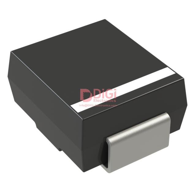
Mechanical characteristics of S3JB-13-F Diodes Incorporated device
The S3JB-13-F from Diodes Incorporated utilizes a molded plastic SMB package, engineered with meticulous attention to mechanical and environmental resilience. The adoption of UL 94V-0 flammability-rated encapsulation not only constrains potential fire risk under thermal or electrical fault but also aligns with rigorous international safety requirements for high-reliability electronic assemblies. Engineers executing thermal risk analyses in compact power systems frequently encounter tighter physical constraints; the assured flame-retardancy of this enclosure streamlines compliance considerations during system certification and layout.
The device's Moisture Sensitivity Level 1 designation per J-STD-020 denotes hermetic resistance to moisture-induced degradation, ensuring that even under extended exposure to humid manufacturing or operation environments, the S3JB-13-F surpasses the requirements typically demanded for automotive or industrial deployment. This robustness obviates the need for special handling or post-reflow baking procedures—a significant benefit during high-throughput SMT production, as process interruptions stemming from moisture-induced popcorn effects are minimized.
Terminal preparation further optimizes for assembly efficiency and reliability. Use of solderable, lead-free matte tin terminals guarantees not only RoHS compliance but also excellent wetting performance, accommodating both lead and lead-free solder chemistries. This provides consistent solder joint formation across varied process profiles and mitigates field failure rates driven by poor metallurgical bonding. The terminal interface meets MIL-STD-202, thus enabling straightforward qualification within defense or aerospace-oriented designs, where both repeatable assembly and enduring field reliability are paramount.
Polarity marking through a cathode band or notch supports rapid visual verification pre-placement, seamlessly integrating into automated optical inspection (AOI) flows. Misplacement of discrete diodes remains one of the more insidious, latent defects during mass population stages, and robust, unambiguous marking directly addresses this risk—especially on densely populated, double-sided PCBs.
Mass specification of approximately 0.093 grams for the SMB footprint, and 0.21 grams for SMC, supplies designers with the quantitative precision needed for system mass budgeting. Applications sensitive to inertia, such as aerospace payloads, vibration-resilient mobile equipment, and high-speed actuation platforms, demand predictable distribution of discrete component mass. Experience shows that early engagement with precise component weight eliminates late-stage integration surprises, directly reducing design iteration cycles while aiding regulatory documentation.
A noteworthy insight emerges from harmonizing package-level robustness (flammability, moisture) with ergonomic assembly features (solderability, marking, mass accuracy): this approach directly streamlines product qualification, reduces recurring failure modes in production, and simplifies cross-team communication. This integrative mechanical design ethos translates into tangible reductions in both field service interventions and system total-cost-of-ownership, particularly when scaled across multi-product engineering programs.
Electrical ratings and characteristics of S3JB-13-F Diodes Incorporated diode
The S3JB-13-F diode from Diodes Incorporated is engineered for efficient rectification in single-phase, half-wave conversion systems operating at 60Hz. Its electrical ratings are calibrated specifically for compatibility with both resistive and inductive loads, presenting robust conduction across standard power delivery profiles. In capacitive load scenarios, an enforced derating of 20% on forward current is recommended to mitigate the heightened stress associated with rapid charging transients. This practice is fundamental to long-term device reliability in circuits with significant energy storage elements, such as power supply input stages.
Thermal management forms a critical aspect of the S3JB-13-F's deployment strategy. The specified junction-to-terminal thermal resistance parameter provides a quantified basis for thermal modeling, enabling designers to calculate junction temperatures with high accuracy when integrated onto copper PCB heat sinks. Empirical experience shows that maximizing copper area beneath the diode yields a substantial reduction in temperature rise under continuous conduction, directly influencing MTTF and safeguarding against thermal runaway. This approach is pivotal when placing diodes in densely populated layouts or within enclosures with limited airflow.
Electrical characterization processes are tightly controlled, with reverse leakage and capacitance measurements conducted at 1 MHz and 4 V DC reverse bias. This ensures each device aligns with predictable response behaviors, which are essential for simulation-based design cycles. Standardizing test conditions directly correlates with reliable SPICE or behavioral model outputs, streamlining analog front-end tuning and enhancing the precision of signal integrity analyses.
The data sheet includes a forward current derating curve, charting permissible current levels across various ambient temperatures. Combined with the typical forward voltage characteristics, these curves serve as a granular design reference, informing designers when extrapolating operational limits under both normal and constrained cooling scenarios. Use in high-vibration or compact environments, where thermal cycling and ambient temperature fluctuations are common, further underpins the need for conservative derating and vigilant temperature monitoring.
Optimally, the S3JB-13-F demonstrates its strengths in bridge rectifier assemblies and power factor correction circuits, where consistency in switching and low leakage currents are prioritized. Integrating the thermal and electrical parameters into the design workflow, including simulation and prototype validation, yields a rectification subsystem with enhanced predictability and reliability. This holistic approach, coupling datasheet insights with practical PCB engineering and real-world application habits, underlines the necessity of tightly controlled load management and thermal planning for modern power conversion designs.
Marking information for S3JB-13-F Diodes Incorporated device
Marking information on the S3JB-13-F device from Diodes Incorporated leverages established industry conventions to optimize traceability, authenticity verification, and inventory logistics across the electronic supply chain. The marking schema comprises a product type code—'S3JB' designating the device series and corresponding SMB package—a structured date code in YWW format for rapid identification of manufacturing year and week, and an additional manufacturer identifier. This layered marking system enables direct correlation between physical devices and their corresponding documentation, supporting root-cause analysis during failure investigations by pinpointing lot-specific production parameters. Through this approach, the risk of counterfeit or misidentified devices integrating into assemblies is significantly curtailed, directly impacting system reliability and compliance with quality assurance protocols.
Device-level marking not only streamlines procurement and incoming inspection workflows but also simplifies field return analysis. For instance, rapid visual verification of the date code expedites isolation of affected manufacturing windows during corrective action processes or product recalls. Clear demarcation of device origin and batch also facilitates advanced inventory control practices, such as first-in-first-out (FIFO), ensuring optimal component aging and minimizing obsolescence risks. Observing the mark under standardized lighting and magnification conditions yields reliable readings, and practical experience suggests that laser-marked codes remain legible throughout extended handling, PCB assembly, and environmental stress.
Integrating marking data into enterprise resource planning (ERP) and manufacturing execution systems (MES) enables granular track-and-trace functionality, linking device serials to procurement, test, and deployment events. The high-resolution mapping thus achieved strengthens transparency throughout the product lifecycle, serving as an enabling foundation for predictive maintenance and warranty analytics. An observed trend is the increasing alignment of marking architectures with emerging digital traceability frameworks, where physical codes are cross-referenced with blockchain or cloud-based ledgers. This convergence facilitates a more robust response to traceability challenges, particularly in safety- or mission-critical deployments.
In summation, the S3JB-13-F marking strategy embodies a multifaceted safeguard within the hardware supply chain. Its role extends from basic identification to forming the backbone of integrated quality and risk management systems, directly supporting the evolving demands of modern electronics manufacturing and lifecycle control.
Package specifications and PCB layout for S3JB-13-F Diodes Incorporated diode
Thorough alignment of package specifications with PCB layout is essential for integrating the S3JB-13-F Diodes Incorporated diode within circuit assemblies. The provided package outline documentation defines precise mechanical boundaries, enabling accurate footprint scaling on the PCB. This dimensional clarity is critical in preventing mounting misalignments and facilitating automated pick-and-place operations with minimal risk of component shift. The recommended pad layout serves as a basis for maximizing solder joint reliability, capacity for current handling, and effective thermal dissipation into the board substrate.
Optimal board-level performance of the S3JB-13-F hinges on correct implementation of these guidelines. Engineers routinely adjust pad geometries and clearances in high-density layouts, trading off PCB real estate against heat sinking requirements and trace routing constraints. Adhering to manufacturer-recommended footprints not only expedites design iterations but also standardizes reflow and assembly processes, leading to increased throughput and reduced defect rates during PCB population. The role of solder mask clearance and pad-to-pad spacing further influences electromigration resistance and manufacturing repeatability. Subtle adjustments in these regions, informed by experience with leaded and lead-free processes, mitigate warpage, tombstoning, and other assembly anomalies.
Reference to the latest documentation from Diodes Incorporated remains a necessary practice, as incremental revisions may introduce dimensional refinements or alternate pad structures to address evolving industry standards. Dynamic adaptation to such updates leverages the synergy between device physics and board design, safeguarding against thermal runaway and ensuring integrity under transient loading conditions. Integration of these components into multilayer PCBs prompts additional considerations, such as optimized via placement beneath the thermal pad and careful planning of copper pour regions for enhanced heat extraction.
The nuanced interplay between package outline accuracy and pad layout design extends beyond basic mechanical fitment, directly impacting the device’s long-term reliability and system-level performance. Strategic footprint implementation underlines robust supply chain interactions, minimizing variability during volume production and supporting advanced inspection regimes. Such diligence, coupled with ongoing dialogue between layout engineers and assembly specialists, proves decisive for the successful deployment of S3JB-13-F diodes in demanding power conversion and protection circuits.
Potential equivalent/replacement models for S3JB-13-F Diodes Incorporated device
The task of sourcing suitable alternatives for the S3JB-13-F device from Diodes Incorporated begins with a precise analysis of its electrical parameters and packaging constraints. The S3A/B–S3M/B series presents a diverse set of candidate models, structured to address a variety of operational domains. These alternatives offer a spectrum of reverse voltage tolerances and average forward current capabilities, allowing selection tailored to the protection, rectification, or power conversion objectives within the circuit architecture. Furthermore, mechanical compatibility—primarily SMB and SMC package formats—dictates the placement flexibility and thermal dissipation profiles, directly impacting layout efficiency and robustness.
Decisions regarding model substitution should initiate at the device parameter intersection, addressing voltage standoff and current carrying needs. For instance, system designs handling transient loads or inductive switching often demand diodes with elevated surge current endurance, prompting consideration of models with enhanced non-repetitive peak current specifications. The contrast between SMB and SMC packaging extends beyond mere dimensions: SMC-bodied components may present improved voltage or thermal characteristics, albeit at the expense of expanded footprint, which could influence high-density PCB layouts or reflow processing profiles.
Incremental improvements may be extracted by leveraging datasheet insights on forward voltage drops and recovery times. For power-sensitive or high-frequency environments, lower forward voltage losses translate into tangible efficiency gains, minimizing ancillary power dissipation during conduction intervals. In practical board-level evaluations, optimizing diode selection extends beyond electrical congruence to encompass parametric drift tolerance over temperature ranges, long-term reliability assessment, and compatibility with surface mount procedures.
Historical observation underlines the merit of pre-emptive validation; direct pin-to-pin swaps rarely succeed without due diligence of rated surge capacity, thermal resistance, and switching speed. Design iterations that incorporate margin buffers for voltage and current can insulate deployed systems against specification shifts or batch-to-batch variation. Additionally, a nuanced exploration of vendor ecosystems may reveal regional sourcing advantages or lead-time differentials, directly shaping component continuity strategies.
Selection matrix methodologies offer clear pathways: mapping the S3JB-13-F against the voltage (VRRM), current (IF), surge (IFSM), and package requirements, then identifying S3A-13-F, S3B-13-F, or S3M-13-F as conditionally compatible candidates depending on the application's stress profile. The approach is iterative; granular verification against current version datasheets and environmental qualification reports secures the desired intersection of price, performance, and reliability.
The pursuit of a well-considered replacement underscores a broader theme within component engineering—striking deliberate tradeoffs between immediate compatibility and long-term platform resilience. Direct functional substitution is rarely sufficient; subtle divergences in electrical and mechanical attributes must be weighed against evolved application expectations. This context-sensitive approach can deliver optimization at system level, ensuring the selected diode not only matches nominal ratings but also aligns with overall product lifecycles and manufacturing imperatives.
Important application considerations for S3JB-13-F Diodes Incorporated diode
Selecting the S3JB-13-F from Diodes Incorporated for rectification and protection applications necessitates a detailed evaluation of its electrical and thermal characteristics in system integration. This fast-recovery diode, recognized for its robust reverse voltage tolerance and low forward voltage drop, aligns well with power conversion stages in switch-mode power supplies, motor drives, and high-frequency industrial switching architectures. Its capability to handle substantial peak repetitive reverse voltage makes it an efficient device for blocking and freewheeling roles, directly influencing circuit efficiency and EMI performance.
A deep understanding of the diode's thermal management requirements ensures operational stability. The junction temperature, influenced by continuous average forward current and peak surge conditions, must remain within prescribed safety thresholds. Effective heat dissipation is achieved by optimizing the copper area surrounding the device on the PCB, as increased copper mass reduces thermal resistance, lowering junction temperature rise during sustained operation. Thermal profiling across the board, especially in tightly packed power modules, typically reveals hotspots, and iterative PCB layout refinements can lead to significant improvements in device longevity and reliability.
Ambient temperature fluctuations impose further stress, particularly in industrial environments characterized by poor airflow or cyclical load demands. The diode’s performance envelope should be derated to account for maximum expected ambient temperatures, ensuring that transient heating events, such as start-up surges or load dumps, do not induce overstress or thermal runaway. This derating is particularly critical when the S3JB-13-F is exposed to capacitive discharge scenarios where inrush current magnitudes can briefly exceed average ratings. Analytical modeling, integrating device SOA (Safe Operating Area) curves with real system load profiles, can preemptively identify risk conditions and guide appropriate snubber or series resistance selection.
Load topology exerts a primary influence on stress distribution across the diode. In configurations that include large bulk capacitance or inductive energy storage, reverse recovery characteristics and the associated dv/dt withstand capability directly affect both device survival and overall system EMI signatures. The implementation of controlled soft-start circuitry and precise selection of commutation strategies can further reduce peak stresses, extending diode service life while minimizing unexpected failure modes attributed to repetitive avalanche or secondary breakdown.
From a regulatory perspective, adherence to manufacturer restrictions is paramount. The S3JB-13-F, per Diodes Incorporated declarations, is specifically excluded from life support and critical care systems. Integration in such environments not only contravenes compliance but may expose systems to unacceptable reliability risks. Standard component traceability, batch screening, and systematic reliability audits should be embedded in procurement and QA workflows to prevent inadvertent deployment in restricted domains.
Leveraging field-driven insights, engineers have observed that overstressing the diode in high-frequency, high-dv/dt environments without sufficient derating often leads to increased leakage current and early thermal degradation. Adopting a conservative approach—selecting a voltage and current rating margin beyond nominal requirements—provably enhances mean time between failures in production systems, especially in mission-critical industrial automation and motor control scenarios. Insightful deployment thus intertwines quantitative device characterization with careful board-level and system-level derating and protection strategies, culminating in resilient, efficient power electronic solutions.
Conclusion
The S3JB-13-F 600V 3A SMB rectifier diode from Diodes Incorporated is engineered to deliver a high level of electrical endurance and mechanical stability, forming a trusted foundation for a wide range of rectification and circuit protection roles. At its core, the device leverages a glass passivated junction, which serves as a critical barrier against thermal runaway and leakage current instability. This design choice elevates long-term reliability, even in demanding thermal and electrical cycling conditions commonly encountered in high-density power modules and compact SMPS topologies.
The diode’s electrical profile—a 600V repetitive peak reverse voltage coupled with a 3A average forward current—effectively handles both steady-state conduction and transient disturbances. The high surge current rating allows it to absorb fault transients such as inrush currents at power-up or downstream short circuit events, contributing to system-level robustness without significant derating. Efficient forward conduction, represented by a low forward voltage drop, minimizes thermal losses and supports higher efficiency targets vital in power conversion and distributed architecture designs.
Mechanically, the SMB (DO-214AA) package offers a balance between reduced PCB footprint and ample thermal dissipation, supported by well-characterized leadframe design. Robust terminal construction and consistent marking streamline automated assembly and inspection processes, mitigating risk in high-mix or rapid production environments. Reference designs indicate careful soldering and pad layout strategies can further leverage the SMB footprint by optimizing thermal spreading and minimizing parasitic inductance, which in turn benefits EMI performance and prolongs solder joint integrity.
From a procurement standpoint, the S3JB-13-F coexists with functionally equivalent SKUs throughout the S3A/B – S3M/B series, allowing drop-in replacements and supply chain agility. This interchangeability is particularly valuable in the context of fluctuating material availability and multi-site manufacturing strategies.
Adherence to application recommendations enables the diode to meet or exceed rated performance in real-world assemblies. Noise-sensitive circuits, for example, benefit from pairing with snubbers or optimized PCB layouts to suppress switching spikes, exploiting the diode’s fast recovery characteristics and stable reverse recovery behavior. In higher current or thermally dense designs, conservative derating and supplemental heatsinking unlock further reliability headroom. These nuanced design approaches, honed through iterative prototyping, support prolonged field operation and minimize failure rates in both consumer and industrial solutions.
Beyond datasheet parameters, the S3JB-13-F’s underlying strengths reflect an alignment between process technology and system-level requirements, making it a versatile building block in contemporary electronic architectures. Its application space comfortably spans power rectification, reverse polarity protection, and freewheeling roles—each benefiting from the device’s proven electrical and mechanical performance envelope. Such attributes underscore the importance of precise diode selection and system-aware integration strategies to achieve not just nominal operation, but sustained operational excellence.


