 >
>


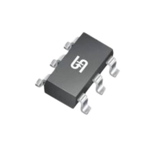
Product overview: DMHC3025LSD-13 Diodes Incorporated MOSFET array
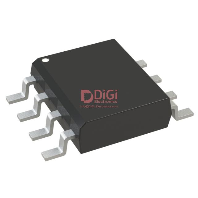
The DMHC3025LSD-13 MOSFET array from Diodes Incorporated exemplifies advanced integration for compact motor drive and power switching solutions. Architected in a standard SO-8 package, the device brings together two N-channel and two P-channel enhancement-mode MOSFETs, streamlining the implementation of H-Bridge topologies. This integrated configuration enables designers to optimize board layout, reduce trace length, and minimize overall system parasitics, which are critical considerations in high-efficiency, space-constrained applications such as brushed DC motor control, miniature actuator drives, and bidirectional switches.
At its core, the balanced pairing of N- and P-channel MOSFETs empowers the device to achieve bidirectional current flow, directly aligning with requirements for DC motor drives implementing full H-Bridge operation. The selection of a 30 V drain-source voltage facilitates reliable performance in medium-voltage regimes, supporting drive currents suitable for a range of industrial and consumer-grade power control scenarios. The integrated nature of the MOSFET array reduces the need for discrete component procurement and matching, thereby minimizing BoM complexity and enabling faster design cycles. The symmetrical internal layout also mitigates device mismatch, which is critical for balancing high- and low-side conduction losses during dynamic load switching.
Thermal management is another layer addressed by the SO-8 package, which provides a sensible compromise between footprint and thermal resistance. Pairing this with optimal PCB copper area under the drain tabs yields effective heat dissipation in densely populated boards, allowing sustained operation and better reliability in confined environments. The device’s enhancement-mode construction delivers low gate threshold voltages, supporting direct logic-level drive and eliminating the need for elaborate gate driver circuitry in most embedded systems. This enables seamless integration with microcontrollers and digital interfaces, vital for real-time motion control and battery-powered portable equipment.
Applying the DMHC3025LSD-13 in practical H-Bridge circuits reveals distinct advantages in terms of waveform symmetry and controllability. Rapid switching between forward and reverse operation minimizes response latency, benefiting feedback-driven speed and position control loops commonly deployed in robotics and precision instrumentation. The device’s low on-resistance parameters further lower conduction losses, allowing for improved energy efficiency and consistent drive authority, especially when operating under pulse-width modulation.
A nuanced aspect of this MOSFET array is its impact on EMC and circuit reliability; the reduced interconnection length and single-package design inherently lower loop inductance and susceptibility to EMI, valuable in environments where compliance and signal integrity are non-negotiable. In field experience, integrating the DMHC3025LSD-13 has translated to reduced debugging hours attributable to pin-to-pin consistency and simplified thermal modeling, streamlining the transition from prototype to mass production.
The DMHC3025LSD-13 emerges as a pragmatic choice where board real estate and system simplicity intersect with demanding performance criteria. The strategic connectivity options permitted by its dual N- and dual P-channel structure introduce design flexibility, supporting both traditional H-bridge modes and more specialized inverter or polarity-switching topologies. Leveraging such compact integrated devices aligns with modern engineering priorities of accelerated development cycles and robust product repeatability, marking a shift from scattered discrete layouts toward modular, application-tuned power architectures.
Key features and technical advantages of DMHC3025LSD-13
The DMHC3025LSD-13 integrates both N- and P-channel MOSFETs into a single compact package, streamlining H-Bridge topologies and enabling designers to substantially reduce board footprint and layout complexity. This tight integration simplifies routing for motor control and load switching, eliminating the need for multiple discrete components while reducing parasitic effects that often impair switching fidelity at high frequencies. Such package-level consolidation proves especially effective in reducing electromagnetic interference and enhancing thermal management due to tightly coupled thermal paths.
The device’s exceptionally low on-resistance (R_DS(on)) directly translates to minimized conduction losses and improved system efficiency. Lower R_DS(on) is structurally achieved through optimized silicon geometry and metallization, ensuring uniform current distribution even under pulsed loads. This characteristic is critical for systems utilizing moderate gate drive voltages, where excessive resistive losses would otherwise compromise duty cycles and thermal margins. Illustratively, performance remains consistent during extended PWM operation cycles, maintaining both energy efficiency and regulatory EMI compliance without the need for additional heatsinking in typical low-to-mid power drive environments.
Input capacitance (C_iss) has been engineered to strike a precise balance between noise immunity and rapid switching dynamics. The reduction in gate capacitance enables faster charge/discharge cycles during transitions, shortening rise and fall times. This mechanism underpins high-speed switch responsiveness, essential in closed-loop motor control or high-frequency PWM-driven circuits; practical implementation reveals reliable position and speed control in compact actuator modules where jitter and overshoot must be tightly regulated. Fast switching characteristics not only support elevated PWM frequencies but enable designers to shrink passive filter sizes, further reducing board space and cost.
Environmental compliance is integral to the DMHC3025LSD-13’s value proposition. The package is manufactured without lead, halogens, or antimony, aligning with global RoHS and environmental directives. This affords compatibility with “Green” procurement strategies and supports reliability in long-life systems—including industrial control panels and precision instrumentation—without sacrifice in mechanical or electrical integrity over prolonged operation.
Automotive-grade reliability forms a cornerstone of the device’s deployment flexibility; strict adherence to AEC-Q101 qualification ensures predictable performance under wide temperature, voltage, and mechanical stress profiles. The DMHC3025LSD-13’s robust qualification enables direct use in harsh environments, such as automotive body electronics, powertrain interfaces, or battery management subsystems. For use cases demanding validated traceability and extended PPAP/IMDS support, the separately designated DMHC3025LSDQ offers full automotive compliance, ensuring seamless alignment with OEM and Tier 1 supplier requirements.
With packaging innovation, optimized conduction efficiency, high-speed switching capability, and proven endurance, the DMHC3025LSD-13 represents a refined solution for engineers targeting compactness, reliability, and regulatory compliance across diverse power drive and control scenarios. Integration at both the device and system level accelerates time-to-market while simplifying qualifying processes—a distinct advantage for agile engineering teams navigating the evolving requirements of industrial and vehicular platforms.
Application scenarios for DMHC3025LSD-13 MOSFET array
The DMHC3025LSD-13 MOSFET array employs an integrated H-Bridge topology within an SO-8 footprint, addressing the increasing demand for high-density, low-loss switching in compact power architectures. Core to its appeal is the complementary MOSFET pair arrangement, which supports rapid bidirectional switching and minimizes parasitic losses. This architecture underpins DC motor control scenarios, where precise speed modulation and directional reversals must translate into reliable actuator motions or energy optimization across mobile robotics and compact appliances. Fast edge performance facilitates fine pulse width modulation, resulting in smooth torque curves and minimized mechanical resonance—key factors for silent operation and long system life.
Integrated inverter designs benefit from the DMHC3025LSD-13’s reduced gate charge and tight channel matching, enabling direct implementation of synchronous rectification or high-side/low-side drive sequences. These properties streamline the assembly of DC-AC conversion stages typical in uninterruptible power supplies, portable energy systems, and motor-driven platforms. By leveraging low Rds(on) and balanced thermal distribution, designers mitigate hot-spot formation on populated boards, a critical challenge in high-frequency conversion applications. The compact SO-8 layout not only shrinks the total real-estate required but also decreases trace length inductance, improving EMI performance and minimizing power dissipation under load transients.
Beyond primary motion and conversion roles, the DMHC3025LSD-13 proves instrumental in rapid load switching, power sequencing, and dynamic energy allocation across embedded and consumer platforms. Attention to gate drive compatibility enables designers to pair the device with low-voltage logic controllers, reducing complexity in multi-rail environments or battery-powered systems. Consistent switching thresholds and controlled gate capacitance offer straightforward timing integration—particularly relevant in industrial automation nodes where deterministic cycle execution prevents jitter or misfire. Thermal concerns previously challenging in small form-factor systems are addressed via efficient conduction path and package-optimized heat spread, supporting extended duty cycles and fault resilience.
Field experience reveals that the device’s integrated configuration simplifies both mechanical and electrical layout, often eliminating external snubber or balancing circuits. This manifests as improved production throughput and fewer post-deployment reliability interventions. The optimized balance between switching speed and current capacity empowers scalable design paradigms—from single-channel modules to multi-axis distributed drives—highlighting a structural shift in system miniaturization without performance compromise.
Critically, the DMHC3025LSD-13 demonstrates that with engineered symmetry, robust switching elements can coexist with demanding power profiles and minimal thermal overhead. Such convergence of compactness, integration, and high-efficiency operation is reshaping how controlled motion and dynamic power management are realized at the circuit level, especially within emerging automation and edge-device domains.
Electrical and thermal performance highlights of DMHC3025LSD-13
Electrical and thermal performance parameters define the DMHC3025LSD-13’s value in applications requiring tightly integrated N- and P-channel MOSFET functionality. The array’s architecture accommodates continuous drain currents up to 6 A for the N-channel and 4.2 A for the P-channel at 25°C ambient, aligning well with the current density demands of contemporary low-voltage power distribution and load-switching tasks. Both channel types sustain a 30 V drain-source rating, encompassing a broad spectrum of logic-level and portable power domains while safeguarding margin against voltage transients and supply variation.
On-resistance, a critical figure in system energy efficiency, is tightly maintained across devices and operating conditions. Tuning R_DS(on) to competitive levels minimizes conduction and switching losses, directly impacting conversion efficiency and thermal load. Empirical data, such as R_DS(on) curves across temperature and current, enable predictive thermal modeling and allow for detailed system-level loss analysis. Such insights translate to concrete design decisions: for instance, in high-frequency DC/DC converters, these curves inform the selection of PCB copper thickness and gate drive timing to fine-tune performance and reliability simultaneously.
Gate drive requirements hinge on well-bounded gate threshold voltages and junction capacitances, which facilitate robust gate-source control with standard PWM controllers and logic ICs. The device’s published threshold spread eliminates ambiguity in turn-on and turn-off design, reducing susceptibility to shoot-through or cross-conduction in bridge structures. Corresponding gate charge and input capacitance data support the optimization of drive current profiles, which is essential in high-speed, low-voltage step-down converters and load switches where nanosecond-scale transitions directly affect signal integrity and EMI.
Thermal performance is engineered around mainstream FR-4 PCB platforms. Maximum ratings reflect practical heat dissipation achieved via common copper pad layouts, and the device remains within comfortable junction temperature limits given prudent via stitching and copper spreading. The design accommodates thermal bottlenecks encountered in dense multi-channel layouts, a scenario frequently faced when integrating multiple loads or parallel MOSFETs to decrease overall system R_DS(on). The guidance provided by thermal resistance values, correlated with empirical PCB stack-ups, has been observed to result in predictable and repeatable thermal profiles, lowering the risk of thermal runaway during extended overloads or output short events.
Electrical characterization employs pulse testing methodologies, decoupling instantaneous electrical specification from the influence of internal self-heating. This approach yields a high-confidence dataset for SPICE modeling and timing analysis, especially relevant for development environments demanding repeatable device behavior under fast switching dynamics. The deliberate avoidance of artifacts from prolonged self-heating strengthens the reliability of simulated worst-case scenarios, a critical factor for safety-critical power path or actuator drive implementations.
The DMHC3025LSD-13’s balanced parameter set underscores its adaptability to space- and efficiency-constrained designs, including battery-protected rails, reverse-polarity guards, and motor actuators. Its engineering proposition lies in predictable, model-driven integration into power paths, with device metrics strongly supporting design-through-verification cycles where simulation fidelity and measured performance must converge without unpleasant surprises. Solid gate control, consistent thermal behavior, and granular electrical data coalesce to reduce design iterations, compress time-to-market, and elevate system dependability.
Package characteristics and recommended PCB layout for DMHC3025LSD-13
The DMHC3025LSD-13 utilizes a molded plastic SO-8 package crafted for high reliability, flame resistance, and streamlined integration within dense PCB environments. The enclosure achieves the UL 94V-0 flammability standard, which acts as a critical safeguard against propagation of electrical faults that could compromise operational safety or device longevity. Selection of “Green” molding compounds underscores consistent RoHS conformity, enabling unrestricted deployment across global markets and simplifying compliance management during mass production.
Terminal construction features a matte tin overlay atop copper, a pairing that prioritizes both chemical resilience and soldering versatility. This configuration interfaces seamlessly with prevalent reflow and wave-solder profiles, resulting in robust, low-resistance interconnects while minimizing the risk of whisker formation and joint degradation over thermal cycles. The leadframe’s surface finish guarantees compatibility with automated pick-and-place systems, facilitating high-yield assembly even under manufacturing variability.
Accurate pad layout engineering empowers designers to leverage full electrical and thermal potential of the SO-8 footprint. Adhering to recommended land-pattern details not only anchors mechanical stability, but also enhances heat transfer paths critical to MOSFETs subjected to elevated currents or rapid switching events. Pin spacing, pad dimensions, and thermal relief layouts—all precisely calibrated by Diodes Incorporated—mitigate solder bridging and enable consistent wetting, directly influencing electromigration resistance and signal integrity. These optimizations often require iterative modeling and prototyping to align board stackup design with system-level power dissipation targets.
In advanced applications, real-world board integration extends beyond basic footprint compliance. Optimizing copper pour strategies and minimizing thermal impedance between active terminals and ground planes reduces hotspot formation and prolongs MOSFET reliability. Trace routing proximity and parallelism enhance noise immunity, particularly important for high-frequency switching circuits. Empirical investigation routinely shows that following manufacturer-specified pad geometries significantly streamlines DFM (Design for Manufacturability) validation and improves rework efficiency.
Comprehensive package and pad reference documentation offers a foundation for precise CAD footprint generation and seamless interoperability with multi-vendor ECAD libraries. This upstream design discipline directly influences downstream processes—from stencil aperture selection to AOI (Automated Optical Inspection) parameterization—producing repeatable outcomes at scale. An insight gained through systematic analysis is that integrating manufacturer specifications with in-field assembly data yields lower defect rates and tight process control. In production scenarios, leveraging the SO-8’s standardization expedites integration with automated test routines and modular carrier systems, evidencing the value of harmonized package selection in multifaceted board design environments.
Strategic use of the DMHC3025LSD-13’s mechanical and metallurgical features, combined with disciplined layout engineering, strengthens both electrical performance and system durability. Practitioners benefit from the synergy between standardized footprints and application-oriented thermal management, confirming the role of package selection as a cornerstone of robust PCB design.
Regulatory compliance and qualification status of DMHC3025LSD-13
The DMHC3025LSD-13 demonstrates a high degree of regulatory compliance, integrating material and reliability standards across multiple dimensions. Engineered in accordance with RoHS3 directives, this component is free of halogens and antimony, positioning it not only as an environmentally responsible solution but also mobilizing its acceptance in jurisdictions that enforce stringent substance controls. By surpassing common compliance and delivering a “Green” status, the component anticipates future regulatory tightening, which minimizes supply chain disruption and reduces the burden on lifecycle management protocols.
A REACH-unaffected designation streamlines procurement and documentation processes. This exemption from extensive REACH candidate list screening and registration accelerates supplier onboarding and decreases administrative overhead in regulated markets. In practice, the absence of REACH-declared substances means device introduction and ongoing use do not trigger additional testing or due diligence, thus shortening time-to-market and facilitating inventory flow, particularly when scaling production or responding to market shifts.
Qualification to AEC-Q101 further anchors the device’s credibility for deployment in automotive and industrial systems where consistent electrical performance under thermal, electrical, and mechanical stress is non-negotiable. The AEC-Q101 standard ensures rigorous high-temperature reverse bias, intermittent operating life, and humidity bias stress tests, among others, conferring measurable risk reduction in mission-critical assemblies. For applications where reliability translates directly to system safety or uptime—such as ECUs, motor drivers, or controller circuits—the DMHC3025LSD-13’s documented screening and lot qualification become cornerstone factors in design-in decisions, especially under IATF 16949-compliant processes.
Moisture Sensitivity Level 1 (MSL1) certifies unlimited floor life in standard ambient conditions, eliminating the need for dry packing or restricted exposure windows at board assembly. This open-ended handling robustness empowers high-throughput surface-mount operations by removing bottlenecks common in lines using higher MSL-rated components. Observations from manufacturing lines indicate that such resilience not only simplifies scheduling but can also markedly reduce logistics and scrap associated with mismanaged exposure or unforeseen delays.
Synthesizing these regulatory and qualification attributes produces a compound effect: risk mitigation, leaner compliance protocols, and operational flexibility. The DMHC3025LSD-13’s compliance and reliability package supports seamless integration into complex qualification matrices, enabling product roadmap agility while simultaneously addressing the increasing intersection of environmental and functional assurance. Its holistic design reflects not just current requirements, but anticipates the convergence of environmental compliance and mission-critical reliability as foundational mandates in next-generation electronics.
Potential equivalent/replacement models for DMHC3025LSD-13
Evaluating alternatives to the DMHC3025LSD-13 requires a systematic comparison centered on core device parameters, beginning with voltage and current ratings. Devices in the same operational envelope—typically in the 30V to 40V range with similar channel current limits—maintain system safety margins and prevent overstress failures. A direct aspect to examine is the dual complementary channel configuration, which supports push-pull or high-side/low-side circuit topologies in space-constrained environments. On-resistance (Rds(on)), an indicator of conduction losses and heat dissipation, should closely match the original device to avoid unexpected efficiency drops or thermal management issues. Close attention to SO-8 packaging enables straightforward PCB footprint compatibility, facilitating rapid prototyping and minimizing mechanical rework.
For applications where automotive compliance is a non-negotiable requirement, the DMHC3025LSDQ variant introduces AEC-Q101 qualification, signifying robust electrical and environmental reliability under extended stress conditions. This qualification is more than administrative—it reflects a device’s survival through rigorous temperature cycling, moisture sensitivity, and electrical overstress validations, ensuring longevity in demanding environments such as engine compartments or power distribution modules. Experience shows that omitting AEC-Q certified components in such contexts often leads to latent reliability hazards, manifesting as field failures or warranty claims.
Standard MOSFET arrays from Diodes Incorporated and peer vendors should be scrutinized by overlaying both datasheet metrics and real-world application data. Beyond headline specifications, nuanced variations in gate charge, switching speeds, and thermal resistance can result in subtle but critical system performance differences. When reviewing alternatives, preference is given to arrays demonstrating consistent low gate threshold variability, which minimizes drive circuit design complexity, and arrays offering robust ESD protection, reducing susceptibility to assembly line mishandling.
Environmental compliance emerges as an operational insurance in modern supply chains. Devices must meet RoHS and lead-free requirements, but practical assessment often includes resilience to humidity and corrosion, which directly impacts long-term reliability, especially when deployed in industrial or outdoor settings.
A crucial but sometimes overlooked factor is the availability of extended documentation support from component vendors, particularly for automotive projects. Experience suggests that models with comprehensive qualification reports and lifecycle management data streamline product certification and enable effective long-term sourcing strategies.
In summary, the alternative selection exercise for the DMHC3025LSD-13 moves beyond surface electrical equivalence—robust engineering practice demands layered analysis of reliability, compliance, and ecosystem support. Pursuing alternatives with rigorous qualification, matched electro-thermal profiles, and robust vendor documentation offers tangible reductions in supply chain risk and design iteration overhead. Industry trends increasingly favor component arrays with modular qualification options and transparent supply histories, prompting a shift toward proactive qualification-centric sourcing rather than reactive spec-matching.
Conclusion
The DMHC3025LSD-13 MOSFET array distinguishes itself with a tightly integrated design tailored for H-Bridge power switching applications requiring compactness and reliability. At the device level, its low on-resistance (Rds(on)) minimizes conduction losses, directly contributing to higher energy efficiency and superior thermal management. Fast switching characteristics, enabled by optimized gate charge profiles, not only reduce dynamic losses but also facilitate precision control in high-frequency motor drive and inverter circuits. These electrical traits, when combined, underpin both performance scaling and system longevity in dense PCB environments.
The array’s architectural integration addresses challenges common in multi-MOSFET discrete approaches, such as alignment accuracy, trace inductance, and interconnect parasitics. By consolidating multiple switches into a single, qualified package, the DMHC3025LSD-13 mitigates common-mode noise and electromagnetic interference, a necessity in automotive and industrial drives where regulatory compliance and robust noise immunity must be balanced with board space constraints. Its AEC-Q101 certification and RoHS compliance guarantee design validity across global automotive and environmental standards, lowering qualification overhead and accelerating time-to-market.
In applied settings, the device supports streamlined implementation of full-bridge and half-bridge topologies, with inherent benefits for both unidirectional and bidirectional load actuation. This positions it as a preferred choice for motorized subsystems—window lifts, seat adjusters, and power tool controls—where tight tolerance requirements and thermal cycles are standard. Procurement and design-in processes are further simplified by consistent supply chain documentation and adherence to mainstream packaging formats, reducing risk during rapid iteration cycles or high-mix, low-volume manufacturing runs.
Practical integration often reveals nuanced system-level improvements—sub-panel consolidation, reduction of assembly steps, and lower potential points of failure—leading to quantifiable gains in overall MTBF (Mean Time Between Failure) of end products. Compounded by the flexibility to address evolving application needs without major PCB redesigns, the DMHC3025LSD-13 enables agile responses to dynamic load profiles or regulatory updates. Its adoption, therefore, reflects a shift toward system-oriented thinking, where component choices align proactively with both technical and operational lifecycle objectives, establishing a baseline for resilient, scalable power management architectures.