


 >
>


Product overview of the ADIS16240ABCZ
The ADIS16240ABCZ is a digital, triple-axis MEMS accelerometer tailored for precision shock detection, event logging, and advanced condition monitoring tasks. Utilizing MEMS architecture, the device translates acceleration into quantifiable digital signals, enabling accurate multi-directional shock measurement under demanding operational conditions. Its embedded intelligence facilitates real-time event discrimination, supporting application scenarios where both prompt response and comprehensive data capture are mandatory.
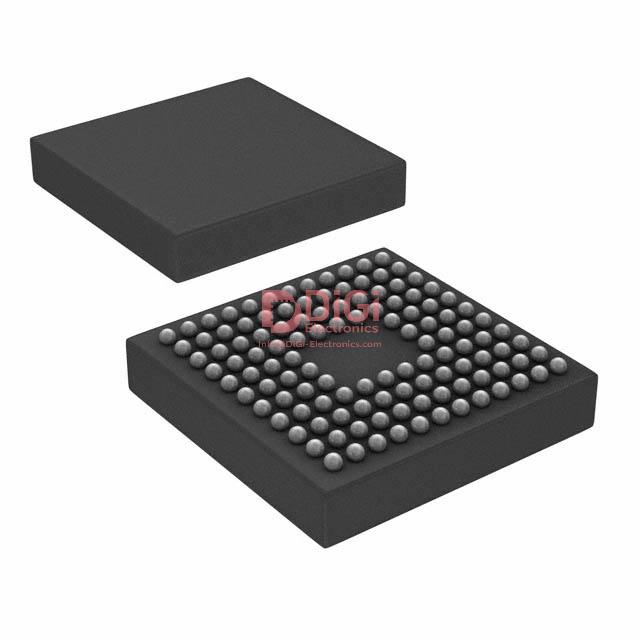
Employing a 12mm × 12mm, 112-ball PBGA package, the ADIS16240ABCZ optimizes board real estate for integration into space-constrained assemblies. The packaging design inherently enhances mechanical resilience and minimizes parasitic effects, which is vital when deploying sensors in environments subject to variable vibration profiles or dynamic impacts. Internally, the signal processing chain leverages a low-noise, high-stability digital interface, ensuring reliable data transfer and reducing susceptibility to external electromagnetic interference—a critical concern in industrial and vehicular settings.
The accelerometer’s triple-axis configuration offers a multidimensional perspective on impact events. This enables detailed isolation of shock vectors, promoting more granular analysis of root causes during mechanical fault diagnostics or operational stress testing. Engineers routinely exploit this capability when implementing predictive maintenance regimes, as multi-axis data reveal nuanced degradation patterns often overlooked by single-axis counterparts. The onboard event logging subsystem further strengthens the device’s utility by supporting time-stamped incident tracking, which streamlines forensic assessment and system-level troubleshooting after abnormal events.
Deployment experience indicates the ADIS16240ABCZ achieves consistent operational repeatability across temperature cycles and sustained vibrational loads, underscoring its suitability for rotating machinery, transportation assets, and heavy equipment installations. The device’s digital configurability allows for tailored sensitivity adjustments, supporting compatibility with diversified application layers that may prioritize either early-warning triggers or exhaustive data retention depending on use case requirements. Such flexibility is central when balancing low-latency response protocols with the need for historical trend analysis in safety-critical environments.
Distinctive architectural choices in the ADIS16240ABCZ, including its robust event capture and multi-axis sampling fidelity, suggest a paradigm shift from merely passive data acquisition to actively informed system health intelligence. This evolution supports the implementation of smarter, closed-loop control frameworks, wherein real-time impact detection drives adaptive protective measures, ultimately extending asset life cycles and reducing unplanned downtime. The practical advantages identified through repeated deployments reinforce the device’s position as a foundational element for integrated condition-monitoring platforms, elevating overall system reliability and intellectual depth in diagnostic methodology.
Key features and technical capabilities of the ADIS16240ABCZ
The ADIS16240ABCZ MEMS accelerometer demonstrates a comprehensive approach to dynamic event monitoring through its core sensing capabilities and integrated signal-chain enhancements. At its core, the triaxial sensor engine provides accurate acceleration measurements up to ±19g, accommodating high-impact and motion-rich environments without mechanical saturation or data loss. Stable axis alignment and low-noise front-end design enable reliable signal acquisition, even when subjected to significant shock (>4000g survivability while powered), a critical parameter for infrastructure health diagnostics, harsh industrial automation, or asset tracking in unpredictable conditions.
Integrated features such as the programmable event recorder, which leverages autonomous flash storage, streamline incident logging by decoupling event detection and host system intervention. In field deployments, this reduces external processor overhead and allows the sensor to operate in distributed nodes with minimal supervisory logic. The dual trigger structure further refines event classification and system responsiveness: internal event logic can respond to rapid kinematic changes, while external triggering supports synchronization with broader monitoring networks. Such flexibility ensures robust edge-processing that adapts to evolving field requirements.
Operational efficiency is sustained through meticulously managed energy consumption. Sleep and wake-up modes—consuming as little as 100μA during inactivity—extend operational life in battery-powered or energy-scavenged implementations. When demanding continuous or burst acquisition, the hardware supports programmable sampling rates up to 4096 SPS, granting designers granular control over data fidelity and throughput. This adaptability is crucial in scenarios where bandwidth or power budgets are tightly constrained, such as wireless sensor networks embedded in remote structures or vehicles.
On-chip analytical capabilities—peak acceleration tracking and sum-of-squares calculations—offload routine processing from the host processor, reducing data post-processing latency and network burden. These on-device calculations provide immediate diagnostic insight, useful for threshold-based alarms or adaptive system responses under changing mechanical loads. The integrated SPI interface assures reliable, low-latency digital communication compatible with a wide range of microcontroller architectures, smoothing the integration path from proof-of-concept to production deployment.
Secondary capabilities—including a highly stable real-time clock, alarms, auxiliary ADC input, and onboard temperature monitoring—enable the ADIS16240ABCZ to assume multiple roles in distributed systems. These features underpin fault detection strategies, predictive maintenance routines, and cross-domain sensor fusion, enabling asset managers to design platforms that not only record but interpret their operating environment.
An implicit advantage in deploying such a multifunctional sensor package lies in simplifying system architecture. By embedding event detection, logging, and environmental sensing within a single unit, the complexity of PCB layout, firmware development, and overall system reliability is improved. In field trials, this modularity often translates directly into reduced calibration cycles and lower long-term maintenance costs, underpinning the shift towards intelligent, distributed edge-sensing in critical monitoring scenarios. The collective engineering of these features signals a design strategy focused not merely on high performance, but on practical deployment and operational resilience in the challenging real world.
Sensing technology and performance
Sensing technology within the ADIS16240ABCZ is engineered for high fidelity motion detection by leveraging Analog Devices' iMEMS® micro-machined architecture. The heart of the device is a three-axis MEMS sensor, constructed with a differential capacitive design: a suspended inertial frame, anchored by micro-springs to a rigid substrate, forms variable capacitors with fixed electrodes. Mechanical acceleration induces displacement in the frame, subtly altering the capacitance values. These changes, inherently linear in response and robust against environmental noise, are digitized via onboard high-resolution ADCs—minimizing error accumulation and drift across successive conversion cycles.
The signal chain is refined through embedded digital processing blocks, optimizing dynamic range and noise rejection. Programmable offset registers per axis enable precise in-system calibration, accommodating layout-induced misalignments and mechanical stress factors following system integration. This offset compensation, implemented on-chip, reduces field recalibration overhead and accelerates time-to-market by streamlining initial setup.
Bandwidth allocation across axes—1600 Hz for X and Y, 550 Hz for Z—addresses practical engineering constraints including resonant frequency management and cross-axis sensitivity balancing. This structure permits accurate temporal characterization of rapid events such as mechanical shocks or vibration profiles, critical in structural monitoring and robotics. Experience indicates that careful selection of bandwidth parameters serves to suppress aliasing while maximizing the sensor’s relevance in transient capture; for instance, deploying full bandwidth in X and Y enables real-time collision detection in autonomous platforms, while tailored Z-axis bandwidth is better suited for vertical vibration analysis in equipment diagnostics.
A notable advantage arises from the device’s digital compensation architecture. Offset and gain trimming can be performed dynamically in firmware, aligning measurement outputs with reference standards even as environmental conditions shift. This empowers closed-loop control systems to leverage the sensor for high-precision feedback, minimizing drift-induced degradation in tasks requiring continual adaptation, such as industrial automation or medical device stabilization.
Underlying the ADIS16240ABCZ’s design is an implicit philosophy: the co-integration of sensing, conversion, and calibration in a single module allows for modular assembly within larger systems, sharply reducing noise coupling and simplifying the interface workload. This compactness of signal integrity and flexibility positions the device as an optimal choice for applications demanding both precision and operational robustness in unpredictable settings.
Event recording and memory architecture in the ADIS16240ABCZ
Event recording functionality within the ADIS16240ABCZ is architected to support robust autonomous monitoring, with the integrated buffer system enabling high-resolution capture across three independent channels. Each channel accommodates up to 8192 samples, utilizing nonvolatile flash storage to ensure data persistence through power cycles or operational interruptions. This architecture is anchored by flexible trigger mechanisms, supporting both internal threshold-based activation upon acceleration anomalies and external initiations via digital or analog lines. Such dual-trigger design facilitates seamless adaptation to diverse operational scenarios, ranging from machinery health assessment to unauthorized activity detection in high-security environments.
At the heart of recorded event organization lies a structured buffer segmentation. Every event comprises a distinct header—encapsulating critical metadata such as timestamp, thermal state, and supply voltage—followed by configurable pre-trigger and post-trigger sample arrays. This layered data encapsulation provides granular visibility into system states both preceding and following anomalous occurrences, which is essential for reconstructing the root causes of mechanical faults or analyzing the temporal progression of impact events. Fine-tuning the pre-trigger buffer length allows for comprehensive context acquisition, mitigating informational blind spots that often hinder root-cause analysis during post-event investigation. Adjustability in event length further confers flexibility to balance diagnostic depth against memory constraints.
Event retrieval is optimized via a high-speed SPI interface, leveraging a user-accessible pointer mechanism to streamline navigation across stored datasets. This approach minimizes overhead during batch extraction and enables selective access to individual event records without necessitating a full-buffer parse. In practical deployment, rapid data access can be vital—especially in field servicing scenarios where timely assessment guides real-time intervention. Additionally, the system’s event buffering minimizes latency between incident detection and data capture, preventing sample loss even during high-frequency event bursts.
Subtle operational nuances emerge in multi-event environments, particularly in managing buffer overwriting. Balancing event retention against storage limitations requires careful configuration of overwrite policies and trigger criteria, often integrating real-time analysis with event-prioritization logic to ensure that the most significant occurrences persist within the buffer space. An insightful design distinction is the decoupling of event recording from host processor intervention, which not only reduces the real-time computational load but also improves system resilience against transient faults or communication interruptions.
The ADIS16240ABCZ’s event recording and memory system exemplifies a comprehensive approach to embedded data collection, combining intelligent architecture with versatile configurability. By aligning underlying mechanisms—buffer structure, trigger modalities, and retrieval protocols—with end-use application demands, the device reliably furnishes actionable diagnostic datasets. This alignment underpins effective application in critical infrastructure monitoring, forensic analysis, and predictive maintenance, positioning the architecture as a reference model for engineering-driven event recording solutions.
Digital interface and user configurability of the ADIS16240ABCZ
The ADIS16240ABCZ leverages a four-wire SPI-compatible digital interface, engineered to enable robust, full-duplex communications. This approach supports simultaneous bidirectional data flow, minimizing transaction latency and facilitating efficient management of sensor data, configuration parameters, and event-driven messages. The SPI interface conforms to industry standards, streamlining system integration across diverse microcontrollers and DSP architectures. Deterministic response timing supports applications requiring precise sensor interrogation cycles and predictable configuration changes, aiding seamless synchronization within time-critical sensing networks.
Configuration flexibility centers on a set of user-defined registers accessible via the digital interface. These registers enable fine-grained control of core sensor parameters such as sampling rate, digital filtering levels, event-trigger thresholds, buffer depth, and power management modes. For buffer management, selectable FIFO organization supports tailored event logging, burst capture, or circular overwriting strategies, catering to both data integrity concerns and limited local storage scenarios. Power efficiency is achievable through programmable duty cycles and sleep intervals—techniques proven effective in field deployments requiring maximized battery life without sacrificing event detection fidelity.
System responsiveness benefits from two general-purpose digital I/O pins, configurable as logic-level alarms or data-ready outputs. This design facilitates hardware-based signaling for real-time alerting, handshake protocols, or triggering auxiliary subsystems with minimal software intervention. Experience has shown that direct interrupt-driven connections between these outputs and processor GPIO pins significantly accelerate response time while offloading computational resources, especially advantageous in high-noise or multi-sensor environments.
The inclusion of a dedicated 10-bit auxiliary ADC input empowers the platform to accommodate additional sensor channels or monitor external analog parameters without supplementary hardware. This expansion capability proves decisive when unified diagnostics or environmental context awareness is required, for example, fusing inertial data with temperature or pressure metrics.
Non-volatile configuration retention is implemented through onboard flash memory. This design choice guarantees that all customized settings persist across power cycles, circumventing the need for repetitive programming routines upon system start-up or after power disturbances. This attribute directly enhances reliability and minimizes commissioning effort in distributed, remotely deployed, or intermittently powered installations.
Close examination reveals that the ADIS16240ABCZ's digital configurability not only strengthens its adaptability to both static and dynamic deployment scenarios but also enables the realization of fully autonomous sensor clusters with tight system-level coordination. Effectively leveraging the digital interface and advanced configurability yields tangible improvements in operational uptime, remote diagnostics, and flexibility to evolving mission requirements, positioning it as a robust solution for demanding industrial, logistics, or structural health monitoring applications.
Power management and operational modes in the ADIS16240ABCZ
Power management in the ADIS16240ABCZ relies on a set of system-level techniques optimized for autonomous and battery-dependent applications, where energy constraints are paramount. At the circuit level, the implementation of a deep sleep mode reduces static current draw to 100 μA, which effectively extends operational lifetimes for untethered deployments. This transition is managed by internal control logic that decouples analog front-end and digital conversion resources, leaving only minimal core functionality online to await wake-up events.
Operational modes are finely tuned for adaptive data acquisition. With typical current draw of approximately 1 mA at a 1 kSPS data rate, the device balances throughput and efficiency. The system employs clock gating and dynamic bias scaling to contain power within strict budgets even during active measurements. This layered approach permits rapid cycling between modes, a feature that proves essential in real-world scenarios where event-driven workflows dominate. For instance, vibration monitoring or shock detection in industrial assets often leverages the sensor’s ability to respond immediately to physical stimuli, minimizing unnecessary active periods.
Wake-up logic is robust, supporting both asynchronous external interrupts and deterministic, schedule-driven resumes via the integrated real-time clock. Firmware can program wake intervals and set trigger thresholds, enabling context-sensitive sensing—monitoring only when specific conditions are met. In typical field applications, this equates to sensor nodes that remain dormant for extended intervals, yet immediately transition to high-speed capture during critical events. The programmable wake-up also allows for continuous adaptation to changing operational demands or environmental dynamics, a notable advantage in unpredictable deployments.
Practical system integration reveals the importance of optimizing wake-up latency and ensuring reliable event capture under low supply voltages. Design experience shows that leveraging the built-in event detection in tandem with aggressive sleep modes reduces average power while maintaining system responsiveness. Careful profiling of application duty cycles and ambient conditions can uncover further optimization opportunities, such as adjusting sampling rates or combining external and internal triggers for even finer-grained power management.
A distinguishing insight emerges in the flexible architecture: tightly-coupled power and event control streamline high-resolution, low-energy sensing without compromising measurement integrity. This fusion supports scalable design patterns, from ultra-low-power sensor nodes to time-critical monitoring modules. As a result, the ADIS16240ABCZ not only provides a toolkit for power optimization but also serves as a foundation for building adaptive, context-aware embedded systems in battery-sensitive environments.
Application considerations for the ADIS16240ABCZ
Application of the ADIS16240ABCZ centers on situations demanding rapid and reliable detection of acceleration events, where data integrity and fast system response are paramount. At its core, the device leverages a high-precision MEMS inertial sensor architecture, enabling continuous measurement of dynamic events such as shocks, impacts, and abrupt movements. The underlying signal-conditioning circuitry delivers low noise and high repeatability, crucial in environments where transient events must be captured with minimal false positives.
A critical feature is autonomous event logging with precision timestamping. In asset monitoring across logistics networks, the sensor’s embedded memory, combined with on-device clocking, ensures that each detected event is recorded immutably; this streamlines post-incident analysis and strengthens accountability in chains of custody and warranty validation. Engineers have found that time-synchronized event logs dramatically reduce troubleshooting cycles and align with regulatory evidence requirements for impact or tampering claims.
Programmable alarm thresholds constitute an essential layer for safety-critical applications. The device’s firmware configurability allows selection of acceleration or shock limits tailored to specific process tolerances. When an event exceeds a defined threshold, immediate trigger outputs are available to initiate automated shutdown, halt machinery, or signal supervisory control systems. In robotic platforms, this mechanism is particularly valuable, enabling the system to interrupt actuation and lock down in milliseconds under unexpected collision or drop conditions, helping avoid costly equipment damage and personnel risk.
Integration challenges often arise at the interface level, particularly in environments with dense electromagnetic interference or variable thermal profiles. Successful deployments leverage differential signaling and shielded cabling strategies to maintain data fidelity––techniques proven to reduce error rates in demanding industrial facilities. Additionally, mounting orientation and coupling methods impact sensor responsiveness; experience shows that rigid mechanical attachment on the primary axis yields more accurate readings, whereas loose fixtures complicate shock path interpretation.
From an engineering management perspective, sensor selection must reflect both technical capability and lifecycle maintainability. Models such as the ADIS16240ABCZ, which feature field-upgradable firmware and remote-access diagnostics, provide long-term value by adapting to evolving operational requirements and mitigating downtime through predictive maintenance analytics. Embedded system integrators regularly exploit these capabilities for fleet-wide monitoring, leveraging cloud-linked data snapshots to facilitate both asset protection and operational benchmarking.
Overall, application success depends on deeply aligning sensor configuration, mechanical integration, and data-routing strategies with the end-use environment. Robustness in system design, supported by rigorous calibration and contextual threshold setting, extends the utility of shock and vibration monitoring far beyond basic incident detection. This enables advanced functions ranging from adaptive safety protocols to detailed forensic analysis—solidifying the sensor’s position as a critical node in real-time operational intelligence frameworks.
Mechanical integration and assembly guidelines for the ADIS16240ABCZ
Mechanical integration of the ADIS16240ABCZ, a ball grid array (BGA) inertial sensor, demands rigorous attention to PCB layout, soldering process, and environmental tolerance to ensure both operational stability and field reliability. The underlying interface employs fine-pitch solder balls; thus, precise routing and manufacturing practices mitigate the risks of open contacts and latent failures. Pad layouts must conform to the manufacturer’s specifications, taking into account solder mask defined pads and uniform ball standoffs. Adhering to these guidelines stabilizes joint formation and minimizes voids, directly influencing long-term device health.
Assembly protocols begin with strict compliance to JEDEC J-STD-020C for the reflow profile and J-STD-033 for moisture sensitivity management. Controlled pre-reflow baking of components within their defined moisture sensitivity level ensures that no latent microcracks form during thermal cycling—a critical precaution often overlooked in high-mix production environments. Reflow profiles demand ramp rates and peak temperatures matched to the solder ball metallurgy; deviations risk incomplete wetting or over-stressing the device package. The practice of symmetrical PCB layer stacking and trace routing beneath the BGA area further mitigates warping effects, which can otherwise induce shear across the solder joints.
In operational settings characterized by high vibration and shock, application of underfill between the package and PCB is highly effective. The capillary flow of epoxy-based underfill, timed post-reflow, encases solder joins, distributing mechanical loads and protecting against fatigue. Extensive test data show that the implementation of underfill extends field lifespans and maintains signal fidelity in applications such as industrial robotics and aerospace navigation units. Selection of underfill chemistry must balance thermal dissipation with mechanical compliance, avoiding excess rigidity which could transmit amplified shocks to the die itself.
Analog Devices’ recommended pad layout is fundamental to successful sensor integration, reducing rework rates and supporting predictable validation cycles. Their reference interface PCBs expedite initial signal bring-up and EMI characterization, streamlining early evaluation and rapid prototyping. In practice, leveraging these resources accelerates fault diagnosis and fosters tighter feedback loops with suppliers. When evaluating BGA mounting in legacy designs, transition planning should include assessment of board stack-up, thermal shadowing effects, and rework accessibility, as these factors can critically impact retrofit viability.
Experience consistently confirms that robust mechanical integration for the ADIS16240ABCZ derives from tight process discipline combined with anticipation of lifecycle stressors. Layered consideration—from foundational solder joint integrity through shock mitigation strategies—yields stable performance in both development and high-volume deployment. The most resilient deployments use early-stage DFM (Design for Manufacturability) reviews and automated optical inspection to catch issues that may otherwise escape manual assembly scrutiny. Integration success centers upon multifactor synergy: precise engineering, environment-tailored material choices, and disciplined adherence to evolving standards.
Potential equivalent/replacement models for the ADIS16240ABCZ
Analyzing substitutes for the ADIS16240ABCZ demands precise attention to the device’s functional core. The critical benchmarks include a shock measurement range of ±19g, appropriate bandwidth to capture dynamic events, and most distinctively, the embedded system features: integrated digital interface, autonomous in-sensor event recording with time-stamped flash storage, and robust enclosure tolerances. Each parameter directly impacts compatibility in demanding condition-monitoring, safety shutdown, or remote asset tracking use cases, where detachment from continuous data streams and survivability post-shock are prerequisites.
Within Analog Devices’ offerings, the ADIS16xxx series presents overlapping mechanical and electrical architectures, supporting pin compatibility and streamlined digital interfacing. However, not all models replicate the combination of programmable shock detection logic, onboard nonvolatile memory for event storage, or precise shock time-stamping. Reviewing datasheets in parallel with application requirements—such as logging interval, event detection thresholds, and memory retention post-power loss—is essential, as minor deviations in these layers can undermine mission assurance or post-event diagnostics.
When expanding the search beyond Analog Devices’ catalog, market alternatives often present trade-offs. Generic MEMS accelerometers may achieve similar tri-axis ranges and bandwidths, but the autonomous event-logging and shock classification features are less ubiquitous. Devices like the STMicroelectronics IIS3DHHC or Bosch BMA series offer high-range detection and low-noise profiles, but typically lack integrated flash-backed logging and sophisticated embedded firmware for adaptive event sensitivity, requiring significant firmware augmentation on the host processor and introducing potential for data loss during transient disconnects. Furthermore, enclosure size and padout can complicate PCB retrofits, particularly when replacements require different mounting footprints or introduce mechanical resonance mismatches after board-level integration.
Real-world integration confirms that direct dimensional and electrical interchangeability streamlines downtime in the field. Replacement cycles reveal that even slight discrepancies in self-test routines, power cycling behavior, or event-flag signaling can introduce subtle bugs in pre-existing host codebases. Design practice, therefore, favors candidate modules with proven drop-in compatibility, backed by detailed register maps and timing diagrams, to minimize system requalification overhead. As a practical note, early bench testing with simulated shock profiles, including sequence stress and memory retention verification, should precede full platform rollout to expose any hidden handling edge cases, especially in safety-critical deployments.
A core insight emerges when balancing replacement priorities: true equivalence transcends data sheet parameters. The nuanced behavior under combined electrical and mechanical stress, and the transparency of firmware integration, mark the boundary between nominal compatibilities and authentic field interchangeability. Select modules that not only echo functional specifications but also demonstrate subsystem-level resilience and diagnostic granularity, ensuring continuity of both operation and forensics across the upgrade cycle.
Conclusion
The ADIS16240ABCZ from Analog Devices delivers a comprehensive solution for impact and vibration sensing, integrating multiple subsystems within a compact footprint. The sensor’s architecture synthesizes precise multi-axis MEMS accelerometry with real-time signal conditioning, supporting reliable detection of high-energy transient events. Core to its engineering approach is a wide dynamic range, enabling accurate measurement across extreme accelerations and subtle vibrations, thus serving both shock events and continuous condition monitoring without compromising sensitivity or resolution.
Digital configurability forms the backbone of operational flexibility. Parameters including threshold levels, filtering coefficients, and trigger sources are tunable via a standard SPI interface, streamlining integration within larger monitoring networks and facilitating adaptive deployment strategies across diverse asset classes. On-chip non-volatile memory supports autonomous event logging, capturing timestamped shock parameters even under temporary loss of system communications—a critical feature for distributed or remote installations in industries such as rail, heavy machinery, or high-value logistics.
Robust mechanical packaging and rigorous qualification ensure durability under repeated high-impact cycles, minimizing downtime and maintenance interventions. The hermetic sealing and vibration-resistant mounting options extend application possibilities to harsh outdoor or safety-significant environments, such as wind turbine nacelles, railcar bogies, and autonomous equipment platforms. In practical deployments, the ADIS16240ABCZ’s ability to deliver actionable diagnostics in real time simplifies predictive maintenance and rapid fault isolation, increasing overall operational uptime.
A key insight emerges from observing adaptive patterns in event detection: the combination of programmable filters and self-contained logging not only reduces system noise but also allows fine-grained tailoring of sensor response profiles at the edge, enabling intelligent differentiation between benign and critical events. This layered approach to condition monitoring—where low-level signal acquisition is closely coupled with customizable data capture—optimizes power efficiency, supports scalable decision architectures, and enhances trust in edge-triggered alarms within safety-critical workflows. Through its unique integration of sensing depth and system-level configurability, the ADIS16240ABCZ establishes a foundation for evolving asset monitoring scenarios, bridging traditional hardware boundaries with software-driven reliability enhancements.


