 >
>


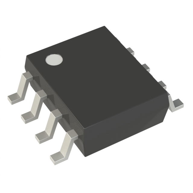
Product overview: VIPER22AS-E STMicroelectronics
The VIPER22AS-E from STMicroelectronics exemplifies a monolithic approach to power conversion in offline switch mode power supply (SMPS) designs, specifically emphasizing flyback topology. Central to its architecture, the device integrates a current-mode pulse-width modulation (PWM) controller and a high-voltage power MOSFET onto a single silicon die, streamlining both the electrical layout and thermal management considerations. This integration minimizes external component count and layout complexity, directly translating into improved reliability, reduced EMI, and compact form factors—a critical set of attributes for space-constrained designs in consumer electronics and industrial subsystems.
Delving into key technical mechanisms, the current-mode control loop offers cycle-by-cycle current limitation and inherent pulse-by-pulse overcurrent protection, ensuring robust response under fault or overload conditions. The controller supports quasi-resonant switching strategies, which, coupled with the onboard high-voltage startup cell, allow efficient operation across wide line and load conditions. The embedded features such as high-voltage startup, undervoltage lockout, and thermal shutdown further reinforce system-level resilience without necessitating supplemental circuitry.
From a packaging perspective, the 8-pin SOIC format caters to automated assembly lines and supports standard PCB footprints, facilitating both initial development and mass production. Real-world applications see the VIPER22AS-E addressing battery charger adapters, standby power supplies in televisions and display monitors, and dedicated auxiliary rails in motor control modules. In such environments, its ability to maintain high standby efficiency and meet stringent regulatory constraints on no-load consumption becomes a significant enabler for compliance-driven product releases.
Practical deployment reveals tangible benefits in stock-keeping simplification and time-to-market acceleration. Designers leverage the integrated MOSFET’s carefully selected breakdown voltage and RDS(on) parameters, ensuring robust operation under global mains variations without derating. The chip’s start-up sequence, governed by the high-voltage cell, reliably eliminates the classic latch-up risks seen in discrete implementations.
A unique insight emerges when considering flyback supply margin optimization. The VIPER22AS-E’s modulation and protection mechanisms interact synergistically to maintain output accuracy and protect downstream circuitry. When designing multiple auxiliary supplies on a common PCB, engineers often exploit the device’s low quiescent current and high-voltage withstand to implement isolated bias rails or independent low-wattage outputs with minimal interference between domains. The result is reproducible, robust designs that scale seamlessly, lending themselves to standardized design platforms across product portfolios.
Advanced users exploit the chip’s flexibility in feedback loop compensation, tuning loop bandwidth to trade transient response against EMI radiated signatures—unifying compliance and performance targets without iterative hardware revisions. The VIPER22AS-E, by consolidating core power conversion and advanced protection in a mature package, continues to anchor efficient and resilient small-form-factor offline power architectures.
Key features of the VIPER22AS-E
The VIPER22AS-E integrates multiple functional blocks and protection features targeted at robust and efficient offline power conversion. At its core, the device operates with a fixed 60 kHz switching frequency, a critical parameter for EMI management. Maintaining a stable switching spectrum simplifies input and output filter design, supporting rapid compliance with international EMC standards without iterative hardware tuning. Consistent frequency operation also narrows the spectrum of conducted and radiated emissions, improving predictability in noise mitigation strategies.
The VDD pin’s wide 9 V to 38 V operating envelope enhances flexibility in auxiliary power architectures. Designers can leverage this range to accommodate different start-up and bias-generation schemes, including direct auxiliary windings or bias from regulated rails. This versatility proves beneficial in both wide-range universal input applications and in systems where supply voltage may fluctuate or ramps during various operating states.
The device’s current mode control serves as a cornerstone for converter dynamics. This architecture enables rapid correction to line and load transients, minimizing output voltage deviations and simplifying compensation network design. The inherent cycle-by-cycle peak current limitation acts as a first line of defense against transformer saturation and power-stage component overstress. This granular control eliminates the need for bulky pulse-by-pulse external protection networks, streamlining PCB layout and reducing bill-of-materials complexity.
Integrated high-voltage start-up circuitry removes the necessity for bulky high-wattage resistors traditionally required to charge the VDD rail at power-up. By using an internal HV start cell, the device curtails inrush currents and improves thermal profiles during initial energization. This approach not only saves board space but also enhances start-up reproducibility across input voltage variants.
Safeguarding against voltage dips on the auxiliary rail, the VIPER22AS-E’s UVLO circuitry employs hysteresis to maintain system stability throughout brown-out and start-up events. Proper hysteresis levels guarantee re-starts occur only under valid power conditions, avoiding erratic controller toggling that can damage power components.
Comprehensive protection features—including overtemperature, overcurrent, and overvoltage—combine with automatic fault restart mechanisms for elevated operational robustness. These strategies substantially increase long-term reliability, particularly in high-availability scenarios where single-fault tolerance is essential. Experience indicates that such integrated fault handling decreases field failure rates and expedites design qualification by obviating the need for discrete crowbar or external latch-off circuits.
A subtle yet impactful advantage arises from the confluence of these features: the VIPER22AS-E not only minimizes external component dependencies but also enables designers to meet stringent safety and efficiency targets with minimal design cycles. The device’s tight integration, predictable behaviors under fault, and flexible auxiliary voltage acceptance streamline both prototyping and eventual mass production, reducing timelines and simplifying production change management. This provides a distinct asset in cost-sensitive or space-constrained SMPS designs, especially where regulatory compliance and rapid time-to-market are decisive.
Electrical and thermal characteristics of the VIPER22AS-E
The VIPER22AS-E exhibits a tightly integrated controller-MOSFET topology, engineered for systems demanding predictable electrical behavior and thermal reliability. The device’s absolute maximum ratings are meticulously defined, constraining voltage, current, and power dissipation boundaries to prevent excursions beyond the silicon’s safe operating area. Under standard characterization conditions—specifically, 25°C junction temperature and 18 V VDD—parameters such as off-state leakage, RDS(ON) values, and switching thresholds are measured to provide reference for real-world design margins.
Detailed examination of startup and operation points reveals the significance of core characteristics like start-up voltage threshold and drain-source overvoltage robustness. These parameters directly impact converter responsiveness and immunity to line transients. The inclusion of precise current limit protections mitigates short-circuit risks by forcing the device into persistent or hiccup mode under fault conditions. Overtemperature protection is implemented via an internal sensor calibrated to threshold points—commonly around 150°C—ensuring automatic device self-protection in scenarios of impaired airflow, board-level thermal bottlenecks, or sustained overload.
Thermal performance is defined not only by intrinsic device features but also by the layout efficiency and copper area on the PCB. The SO-8 package geometry, when employed on a 200 mm² FR4 copper footprint, enables a manageable thermal resistance to ambient. Practical deployments highlight that copper planes must be optimized for both electrical conductivity and heat spreading, especially in applications with space constraints or elevated ambient conditions. Placement within enclosures or proximity to other dissipative elements necessitates a holistic thermal budget analysis. Empirical observation points to enhanced longevity and reduced derating penalties when the board layout adheres strictly to datasheet recommendations, underscoring the importance of thermal simulation during early-stage design.
Unique to the VIPER22AS-E are the tightly coupled electrical protections, which simplify compliance with international safety standards for isolated flyback and auxiliary rail supplies. The robust SO-8 synergy with internal safety features offers system architects a deterministic platform for rapid prototyping and reliable mass-market deployment. The consolidated controller-MOSFET architecture shrinks solution real estate and minimizes failure points, translating to higher mean time between failures (MTBF) in both commercial and industrial installations.
Strategic thermal engineering—prioritizing well-distributed copper, effective via stitching, and adequate airflow—directly correlates to device dependability. Overlooking PCB design nuances, particularly in high-density assemblies, accelerates thermal stress and latent device degradation. Thus, systematic focus on both electrical limits and practical board-level thermal management is not only recommended but essential for leveraging the full potential of the VIPER22AS-E in advanced power conversion scenarios.
Pin configuration and functional description of the VIPER22AS-E
The VIPER22AS-E’s 8-pin configuration is engineered for efficient integration within isolated and non-isolated switch-mode power supply topologies, especially where compact layout and minimal external component count are prioritized. At the schematic level, the allocation of specific functions to each pin supports optimized circuit partitioning: the Drain (DRAIN) pin connects directly to the high-voltage DC input, facilitating both startup current injection and power-switch conduction. This dual-use arrangement reduces the need for auxiliary startup circuits, leveraging intrinsic device robustness while streamlining power stage assembly.
The SOURCE pin establishes the primary return path, ensuring controlled switching behavior and maintaining reference potential consistency. Close attention to trace impedance and grounding at this node minimizes EMI emissions, a practical improvement noted during EMI compliance iterations. The internal control section, interfaced through the VDD pin, is powered from an auxiliary winding or bootstrap arrangement. This pin’s undervoltage and overvoltage thresholds tightly regulate controller operation and contribute directly to system stability across a wide input range.
The FB (feedback) pin offers high sensitivity to feedback loop perturbations. When tied to the secondary-side feedback circuit via an optocoupler, minute voltage changes effect precise duty-cycle modulation, delivering reliable output voltage regulation under dynamic loading conditions. Incorporating the FB input with external compensation elements allows control-loop bandwidth optimization, a critical aspect for reducing startup overshoot and response times in fast transient designs.
To manage overload and short-circuit events, the VIPER22AS-E leverages its current sense and internal clamping mechanisms. Pin allocation enables rapid fault reporting, and the controlled shutdown process protects both the device and connected circuitry. Comparative lab tests demonstrate that proper PCB layout—ensuring short, low-inductance connections to the current sense and power path pins—reduces false triggering and enhances fault immunity, reflecting the practical value of layout discipline mandated by pin configuration.
In the context of transformer-coupled architectures, the pinout accommodates both flyback and primary-side regulation approaches, allowing support for a variety of output requirements without board re-design. The direct link between power switching pins and external transformer elements minimizes propagation delay and thermal hotspots, underpinning robust thermal management in real-world deployments.
The natural mapping between function and pin assignment in the VIPER22AS-E does more than facilitate error-free assembly. It also creates a foundation for scalable SMPS solutions, enabling migration between power classes with minimal learning curve. Careful attention to these physical and functional relationships amplifies the practical reliability and flexibility of the end design, reinforcing the device’s utility in both rapid prototyping and high-volume production scenarios.
Core control and operation mechanisms of the VIPER22AS-E
At the heart of the VIPER22AS-E lies a current mode PWM controller optimized for tight regulation and responsive dynamic behavior. The internal control loop governs switch conduction based on sensed oscillator cycles and instantaneous current feedback, ensuring each output pulse adheres closely to programmed parameters. Unlike conventional voltage-mode strategies, the device constantly analyzes the primary current waveform, offering enhanced stability against supply perturbations and load transients. This methodology is particularly effective in switched-mode power conversion where both over-current protection and output voltage consistency are paramount. It suits battery charging topologies and auxiliary power rails that require sharp current thresholds and well-defined voltage setpoints.
Integration flexibility is a core strength of the VIPER22AS-E architecture. The device’s open-loop output configuration can be seamlessly enhanced through addition of external signal conditioning—such as the coupling of high-accuracy reference devices and dual operational amplifiers. Designers often integrate parts like TSM101 for combined voltage and current feedback, tightening output regulation and providing synchronous correction cycles. Experience demonstrates that this approach yields rapid load response while mitigating risk of output overshoot, particularly in systems with mixed analog and digital domains.
The VDD pin’s broad admissible voltage span, ranging from 9 V to 38 V, equips the device for reliable operation across diverse input environments. In engineering practice, this is essential for universal input AC/DC adapters, where cold starts and supply dips can cause unstable behavior in lesser integrated controllers. The embedded high-voltage current source on the VIPER22AS-E initiates bias rapidly without external circuitry, ensuring clean, repeatable start-up even from subthreshold conditions. This removes the dependency on bulky discrete charge pump blocks, streamlining board space and reducing total BOM cost.
Feedback signal processing in the VIPER22AS-E deviates from classic voltage amplification approaches. The controller monitors the feedback pin as a current input, increasing modulation resolution and fostering finer output adjustment. This direct current sensing facilitates sensitive, proportional burst mode entry under light load, balancing low standby consumption with fast recovery to full-load operation. Such adaptive burst behavior meets regulatory demands for standby efficiency without sacrificing transient performance—a design priority in modern consumer and industrial power subsystems.
Protection mechanisms are deeply embedded. Any overvoltage event on VDD instantly engages an auto-reset/restart sequence through an autonomous internal controller block. This design eliminates extended current stress on switching devices during fault conditions. Real-world deployment showcases significantly reduced field failure rates and predictable restart cycles after fault clearance, marking a shift toward self-healing power electronics with minimum intervention.
In summary, the VIPER22AS-E sets a reference point for high-efficiency, controllable, and robust power conversion. Its layered mechanism—from granular current mode control to sophisticated start-up and protection strategies—enables seamless integration into complex applications, supporting stringent reliability and regulation requirements. This architecture embodies a shift toward automated, efficiency-driven, and application-adaptable power design, forming the backbone for next-generation SMPS implementations.
Application considerations and typical use cases for the VIPER22AS-E
Application of the VIPER22AS-E centers on high-efficiency, low-power AC/DC conversion, addressing the stringent requirements of contemporary electronic designs. At the circuit level, the device integrates a PWM controller with a high-voltage power MOSFET, minimizing the external component count. This integration enables compact designs and streamlines EMI compliance. Such architecture is especially beneficial for systems with limited PCB space or layouts where noise mitigation is essential.
In battery charger adapters, precise management of current and voltage is critical. The VIPER22AS-E supports secondary-side regulation architectures, facilitating constant-current and constant-voltage charging profiles. This is particularly important when dealing with advanced battery chemistries prone to overcharging or deep discharge. The IC’s capability for reliable feedback control simplifies the implementation of protection features, such as thermal shutdown and overvoltage protection, reducing development cycles and long-term maintenance.
Auxiliary and standby power supplies for consumer electronics—like TVs, monitors, and set-top-boxes—leverage the VIPER22AS-E’s low quiescent consumption and burst mode operation. Such features help meet increasingly strict international energy regulations, including standby power limits below 0.5W. In this class of applications, maintaining rapid wake-up from standby is key to user experience, a requirement met by the device’s fast recovery characteristics.
Within industrial and building automation, auxiliary switch-mode power supplies often operate in electrically noisy environments and must tolerate broad input voltage variations. The VIPER22AS-E’s wide input range and robust short-circuit and overload protections make it well suited for these scenarios. The device’s high-voltage startup capability eliminates the need for bootstrap circuits, thereby enhancing long-term reliability and reducing both assembly and bill-of-material costs.
In practical deployment, engineers benefit from the IC’s comprehensive protection mechanisms, which quietly mitigate risks arising from abnormal line or load conditions. For example, the built-in thermal regulation and brownout protections are effective in reducing field failures, especially in geographically diverse installations or where line quality is inconsistent. Systems designed with the VIPER22AS-E often exhibit measurable improvements in meantime-between-failure metrics, especially when board layout and transformer selection follow best practices for creepage and clearance.
The adaptable feature set and minimal peripheral requirements empower rapid iterations during prototyping and support flexible supply design—allowing a single core design to address varying output voltages or power levels. This modularity shortens time-to-market and enables a unified approach across product families. The design philosophy embodied by the VIPER22AS-E reflects a convergence between integration, efficiency, and safety, making it a go-to solution for engineers prioritizing both performance and robustness in low-power AC/DC applications.
Mechanical and packaging details for the VIPER22AS-E
The VIPER22AS-E integrates robust mechanical and packaging features to optimize automated assembly and high-density board layouts. Delivered in the widely adopted 8-lead SOIC package, the device streamlines pick-and-place operations and reflow soldering, mitigating handling risks and enhancing throughput in surface-mount production lines. Dimensional uniformity and adherence to JEDEC standards simplify footprint design, fostering interchangeable layouts across different supply configurations.
Environmental compliance is embedded through ST ECOPACK® standards, supporting lead-free soldering and reinforcing reliability under diverse operating conditions. The mechanical outline has been engineered for precise alignment, ensuring minimal placement error and securing thermal pathways from silicon to PCB copper. This approach reduces junction obstruction, promoting effective heat dissipation even within constrained enclosure geometries.
The SOIC package, with its favorable height and pad pitch, not only conserves PCB real estate but also allows designers to cluster critical components with minimal loop area, reducing electromagnetic interference and parasitic losses. The thermal profile—optimized via leadframe design and mold compound selection—enables consistent performance at varied ambient temperatures. When implementing high-efficiency switching supplies in dense consumer or industrial designs, the package’s synergy of compactness and thermal capability often yields stable outputs without the need for elaborate cooling enhancements.
Experienced implementations reveal that careful solder pad dimensioning and copper pour arrangement are decisive for extracting maximum thermal performance from the package. Applying thermal vias strategically beneath and around the device further improves conduction to ground planes, while conformity to mechanical tolerances streamlines production inspection stages. Notably, the robust mechanical definition of the VIPER22AS-E supports stress resilience during board depaneling and post-assembly transport, reducing latent defect risks in volume applications.
Selecting this package for demanding switched-mode power supply designs accelerates layout iteration and simplifies regulatory approvals, as mechanical and environmental compliance hurdles are effectively managed up front. The package’s balanced design—offering both assembly efficiency and thermal competence—distinguishes it as a preferred solution in rigorous miniaturization and reliability scenarios.
Potential equivalent/replacement models for the VIPER22AS-E
Evaluation of functional replacements for the VIPER22AS-E centers on topology compatibility, key functional parameters, and integration level within the target application. The VIPER22AS-E, an off-line high-voltage converter in SO-8 packaging, is frequently chosen for its monolithic integration of a PWM controller and power MOSFET, simplifying power stage design in AC-DC power supplies. Within its family, options like the VIPer22ADIP-E offer a direct electrical and functional match with an alternate PDIP footprint. This variation in package should factor into decisions involving board layout adaptability, assembly automation, and thermomechanical reliability. Pinout congruency and equivalent creepage/clearance are also critical in high-voltage environments, with specific attention to safety standard adherence.
Broader search for replacements extends to primary switchers with equivalent ratings on start-up current, breakdown voltage, switching frequency, and inrush protection. Practical assessments often reveal subtle yet impactful differences in protection features such as brownout sensing, thermal shutdown thresholds, and integrated EMI filtering, each affecting end system robustness and compliance. Controller topology—whether current-mode or voltage-mode—is essential, as variations yield marked differences in transient response, output ripple, and system stability, especially under varying line and load conditions. Devices from alternate vendors may emulate the functional block diagram, but secondary-side regulation, soft-start behavior, and external component requirements can diverge, influencing bill of materials and qualification time.
From an assembly perspective, package selection intertwines with thermal performance and manufacturability. Compact SO-8 packages facilitate high-density layouts but can constrain heat dissipation, making the DIP variant preferable where natural convection is limited or robust solder joint reliability is needed. Practical experience highlights the advantage of maintaining pin-compatible footprints on PCBs, enabling iterative qualification of various sources without repeated mechanical redesigns. In global supply chains prone to lead time fluctuations, favoring widely supported footprints and cross-referenced part numbers can expedite risk mitigation.
Substituting across manufacturers, close scrutiny of datasheets for undervoltage lockout tolerances, peak MOSFET current capabilities, and recovery time of protection circuits is recommended. These parameters, often stated similarly, may yield divergent results during abnormal grid events or inrush, impacting overall appliance safety margins. In some instances, replacement parts introduce microcontroller-friendly features such as enable pins or fault flags, presenting opportunities for improved diagnostics or remote reset without increasing part count.
A layered replacement strategy—prioritizing the same family for effortless qualification, then exploring external equivalents for greater flexibility—supports robust engineering decision making. Ultimately, the integration density and protection depth of the VIPER22AS-E set a baseline in AC-DC converter designs; any replacement must align not only in headline electrical ratings but also in nuanced system-level behaviors to assure steady-state performance, compliance, and long-term maintainability.
Conclusion
The VIPER22AS-E from STMicroelectronics exemplifies a tightly integrated approach to offline flyback power conversion in low-power domains, bringing together a current mode controller and high-voltage MOSFET within a single, compact device. This monolithic integration addresses several layers of engineering complexity by reducing PCB footprint, eliminating interconnect parasitics, and minimizing the external component count—key parameters for scalable, cost-effective design workflows in contemporary power supply engineering.
Focusing on the underlying mechanisms, the device leverages primary-side regulation with an embedded peak current mode control loop. This architecture enables fast transient response and intrinsic cycle-by-cycle current limitation, thereby mitigating the risk of transformer saturation and excessive primary currents under fault or surge events. The scheme's inherent linearity simplifies control loop compensation, which, combined with comprehensive integrated protections such as overvoltage, overload, and thermal shutdown, results in designs that maintain high levels of operational safety without external supervisory circuits. Notably, the VIPER22AS-E's start-up circuitry operates directly from rectified mains, reducing pre-load and standby losses—a key factor in achieving stringent energy efficiency targets.
The device demonstrates significant versatility in auxiliary output voltage configurations. By supporting both non-isolated and feedback-regulated isolated topologies, it accommodates a breadth of application scenarios, ranging from household appliances and metering equipment to industrial auxiliary supplies. The feedback input is designed with wide tolerance, simplifying the use of both optocoupler-based and primary-side regulation methods. This characteristic allows for flexible adaptation in products where secondary voltage accuracy or feedback insulation levels are dictated by regional or application-specific safety standards.
In practical deployment, the highly integrated VIPER22AS-E significantly accelerates time-to-market. Circuit designers benefit from a mature, application-rich documentation suite, including proven reference designs covering variable input ranges and load profiles. Implementation and troubleshooting time is further reduced by the availability of streamlined bill-of-materials lists and clear PCB layout examples that anticipate electromagnetic compliance and thermal management requirements. Across various design iterations, the platform demonstrates consistent EMI/EMC compliance, even in compact enclosures, thanks to the controlled switching behavior and minimized loop areas.
Examining supply chain dynamics, the device’s established market presence ensures stable procurement and support channels. The maturity of the VIPER22AS-E not only lowers project technical risk but also enables second-source strategies and rapid response to evolving compliance mandates. From a lifecycle perspective, design standardization around such integrated ICs improves maintainability and facilitates long-term field reliability, reducing warranty interventions and contributing to sustained operational uptime in deployed systems.
Integration at this level fosters a holistic approach to power management, transcending mere functional aggregation. The VIPER22AS-E streamlines regulatory compliance, operational robustness, and development agility, underscoring a design philosophy that aligns closely with the demands of modern, scalable, low-power electronic systems.