 >
>


Product overview: STM32L412RBT6P microcontroller by STMicroelectronics
The STM32L412RBT6P microcontroller, positioned within the STM32L4 family, incorporates a 32-bit ARM Cortex-M4 core with an integrated floating point unit (FPU), enabling robust digital signal processing at low energy thresholds. The core's ability to operate at frequencies up to 80 MHz allows for high-throughput computations required in real-time control, signal analysis, and data pre-processing scenarios, without compromising on power consumption. The microcontroller’s ultra-low-power design leverages advanced manufacturing processes and architectural strategies—such as dynamic voltage scaling, multiple low-power modes, and a tightly coupled DMA controller—which collectively minimize active and standby power draw. In practical terms, this means sensor nodes and wearable endpoints can sustain extended operation on compact or single-cell batteries, often exceeding the operational longevity achievable with prior-generation MCUs.
On-chip memory resources are pragmatically balanced: 128 KB Flash and 40 KB SRAM enable efficient code execution, complex algorithm storage, and frequent real-time data buffering, while supporting over-the-air update scenarios and secure data retention. The Flash’s endurance characteristics are well-suited for embedded firmware updates, and the SRAM partitioning facilitates memory-hungry computation, such as real-time filtering or sensor fusion, especially in resource-constrained environments. Peripheral integration is broad, encompassing flexible I/O, multiple communication interfaces (SPI, I2C, USART), and advanced analog capabilities such as a 12-bit ADC, DAC, and fast comparators. This breadth ensures seamless integration with diverse subsystems—actuators, analog front ends, and connectivity modules—enabling adaptable design architectures for application-specific requirements.
Thermal and electrical robustness is maintained through a wide operating voltage envelope (1.71V–3.6V) and an extended temperature rating that reaches up to 125°C, paving the way for deployment in harsh industrial infrastructures and mission-critical medical contexts. Such range ensures reliable operation adjacent to power circuitry, within sealed medical instruments, or inside environmental monitoring devices exposed to rapid ambient shifts. PCB layout and assembly flexibility is enhanced through a 64-pin LQFP package (10x10mm), which strikes a balance between pin availability for feature-rich designs and manufacturability on both commercial and custom board layouts.
From a firmware and system integration perspective, the STM32L412RBT6P’s support for ARM’s ecosystem delivers a streamlined development workflow, whether using STM32CubeMX for peripheral configuration or leveraging standardized middleware for connectivity protocols and security. Developers often exploit the device’s built-in hardware cryptography and secure boot features in sensitive application spaces, reflecting ongoing trends where both energy efficiency and cybersecurity are considered design prerequisites. In deployment, deterministic performance—stemming from the FPU and high-speed core clock—translates to improved response times for closed-loop controls or real-time patient signal acquisition, ultimately elevating product competitiveness, especially in markets driven by miniaturization, reliability, and innovation.
The STM32L412RBT6P thus demonstrates how microcontroller evolution blends hardware efficiency, scalable connectivity, and real-world deployment insights to address the stringent demands of next-generation embedded applications. Its architecture highlights the intersection of low-power strategies with advanced processing, setting a strong benchmark for engineering teams tasked with compact yet intelligent edge computing solutions.
Core architecture and performance highlights of STM32L412RBT6P
At the foundation of the STM32L412RBT6P lies the ARM Cortex-M4 core, a processor architecture that expands beyond basic microcontroller functions by embedding DSP instructions and a single-precision FPU. This enables highly efficient real-time signal processing directly on the device—crucial for applications involving sensor fusion, waveform analysis, or closed-loop control. By implementing hardware support for multiply-accumulate operations and floating-point arithmetic, the Cortex-M4 engine minimizes both computation latency and power consumption compared to software-only algorithms running on simpler cores.
The device further leverages performance through its Advanced Real-Time (ART) Accelerator™. Flash memory, often a substantial execution bottleneck due to limited access speed, is mitigated by deep prefetch logic and instruction speculation. The ART Accelerator™ enables the core to fetch instructions with near-zero effective wait states even at 80MHz, maintaining deterministic throughput invaluable for hard real-time systems and timing-critical loops. Performance metrics—100 DMIPS and 273.55 CoreMark—demonstrate competitiveness with higher-class MCUs, positioning the STM32L412RBT6P as well-suited for precision instrumentation, portable data acquisition, and industrial automation.
Robustness in embedded design is reinforced by the Memory Protection Unit (MPU) combined with up to eight configurable memory regions. Constraining code and data within exclusive address boundaries enables isolation of safety-critical tasks and prevention of accidental data corruption by errant routines. This architecture aligns with best practices in embedded safety—particularly in firmware architectures that split control, diagnostics, or communication into separate software modules. For use cases like medical instrumentation or distributed sensor nodes, such hardware-enforced access control is instrumental in achieving regulatory compliance and predictable fault containment.
In practical deployment, the microcontroller’s combination of DSP/FPU, flash acceleration, and region-based security simplifies integration of complex control logic with responsive real-time behavior. For example, direct implementation of digital filters or sensor calibration routines on the Cortex-M4 reduces external component count and design complexity. Application experience reveals that configuring ART for optimal prefetch size and aligning time-critical ISR code to reside in flash regions optimized by the accelerator create measurable system throughput gains while maintaining tight latency guarantees—a decisive factor when migrating legacy codebases or scaling to higher functional safety levels.
A strategic insight emerges: The STM32L412RBT6P exemplifies a shift in mainstream microcontroller architectures, where sophisticated memory management, integrated computation offload, and deterministic performance are delivered at low power and form factor. This integration is reshaping embedded design patterns, enabling direct deployment of advanced algorithms within power-constrained or space-limited product classes, thus bridging the gap between traditional microcontrollers and specialized signal processors.
Integrated memory and data protection capabilities in STM32L412RBT6P
Integrated memory and data protection in the STM32L412RBT6P leverage a tightly coupled architecture optimized for secure embedded applications. The microcontroller leverages a consolidated 128KB single-bank Flash module as primary code and data storage, while the 40KB total SRAM is divided into 32KB SRAM1 and 8KB SRAM2, enabling differentiated memory access and retention strategies. Both Flash and SRAM are covered by granular access controls, which are enforced by hardware rather than firmware alone, substantially reducing attack surfaces exposed by software vulnerabilities.
Readout Protection (RDP) is implemented in adjustable levels, with fine-grained options facilitating tailored security postures. At the lowest level, flash contents remain accessible for debugging, quick iteration, and field upgrades, promoting ease of development. Progressing to higher RDP levels, the device disables both debug and boot ROM access, ensuring that proprietary intellectual property cannot be extracted, even via sophisticated physical attack vectors. Proprietary Code Readout Protection (PCROP) operates at the sector level, anchoring a critical defense layer for algorithms or data sets with stringent confidentiality requirements. The ability to designate and lock regions within Flash for PCROP mitigates risks associated with supply chain exposures by restricting data exfiltration from defined sectors during operation or reprogramming.
Supplementary write protection options reinforce flash immutability at the granularity of sectors or total space. This is pivotal in systems that demand operational stability, such as automation controllers or medical devices, preventing both accidental and malicious rewriting of validated code images. The integrated Firewall module enables dynamic partitioning of memory, programmatically isolating sensitive regions from unpredictable or untrusted code execution paths. This architectural choice supports robust compartmentalization: an essential principle in modern embedded security frameworks.
Reliability for non-volatile storage is amplified with hardware-accelerated Error Correction Code (ECC), continuously detecting and correcting single-bit failures during flash access. ECC minimizes the risk of latent data corruption, which can undermine system logic or compromise updates. In practical deployment, ECC allows confident operation even under noisy power environments or high-radiation conditions. SRAM2 is equipped with parity checking, immediately flagging bit-level anomalies in high-speed data operations. The provision for data retention in SRAM2 during low-power (Stop and Standby) modes maintains context across power cycles, optimizing rapid resumption in safety-critical systems.
Careful partitioning of memory and the integration of multiple, complementary protection mechanisms within the STM32L412RBT6P illustrate a layered security paradigm. When designing for mission-critical environments, direct mapping of these features onto application demands—such as storing cryptographic keys in PCROP-protected Flash or utilizing the Firewall to isolate firmware update routines—delivers measurable improvements in system resilience. Device reliability, long-term maintainability, and regulatory compliance are each bolstered by these holistic protections. In operational scenarios, empirical tuning of access control levels and error correction settings demonstrates a trade-off between debugging flexibility and ultimate security, requiring iterative calibration to achieve optimal balance. Adopting a defense-in-depth strategy, as supported by this microcontroller, reflects contemporary engineering best practices where security, reliability, and functional integrity coalesce within embedded platforms.
Power supply architecture and ultra-low-power modes in STM32L412RBT6P
STM32L412RBT6P incorporates a highly adaptable power supply architecture, providing granular control over energy consumption across diverse functional blocks. The device features dual power provisioning options: direct SMPS interfacing for optimal conversion efficiency at reduced core voltages (within 1.00–1.32V range), as well as internal low-dropout linear regulators that simplify legacy integrations and maintain supply integrity for specific regions. Domain-based configuration allows isolation of analog, USB, and backup/RTC domains, optimizing noise immunity and minimizing inadvertent power draw in precision sensing environments or when USB functionality is dormant.
The ultra-low-power operational capabilities are anchored in the microcontroller’s flexible state management. Up to seven discrete power modes are available, enabling dynamic tailoring of system consumption to workload requirements. Transitioning into Shutdown mode minimizes residual currents to 16nA; such deep sleep states are critical for extended battery lifetime in autonomous monitoring systems. In practical deployment, leveraging the Stop mode’s microsecond-scale wake-up latency (~4μs) becomes indispensable for applications requiring event-driven responsiveness—realizing low-power always-on listening with immediate context restoration for active data processing or wireless transmission.
VBAT functionality ensures that backup registers and the real-time clock persist seamlessly, irrespective of main rail availability. This architecture supports robust retention designs, particularly in data-logging or time-stamping scenarios where power interruptions are frequent—a feature field-tested in industrial sensor modules operating on coin cells in remote installations. Redundant supply paths and intelligent power gating schemes further allow subsystem prioritization, balancing background housekeeping against core application throughput.
A subtle yet effective strategy involves exploiting selective peripheral gating and memory retention across modes, which permits designers to maintain critical configuration states while sidelining nonessential blocks. This fine-grained management, layered atop foundational supply architecture, enables significant power savings without loss of system coherence—a unique edge in competitive designs targeting wearables, portable instrumentation, or IoT endpoints subject to stringent energy budgets.
The integration of multiple low-power options and independent supply rails confers on the STM32L412RBT6P a flexible platform for both prototyping and mass production, particularly where real-time performance must coexist with long-term autonomy. The device’s architecture encourages iterative refinement of power management schemes, underpinning scalable solutions from proof-of-concept to deployment while accommodating unforeseen power anomalies or edge case requirements inherent to field use.
Peripheral and communication interface features of STM32L412RBT6P
The STM32L412RBT6P incorporates a comprehensive suite of communication and peripheral interfaces, engineered to address the multifaceted requirements of advanced embedded systems. Its architecture is shaped around flexibility, high data integrity, and minimized power consumption—critical for applications demanding reliability and efficiency in resource-constrained environments.
Examining its I²C capability, the device offers three separate channels—each fully compliant with SMBus and PMBus protocols. Fast-mode plus support extends bandwidth up to 1 MHz, permitting rapid sensor acquisition or inter-IC communication, particularly vital in distributed control or monitoring systems. Dynamic wake-up mode enables instantaneous reactivation from low-power states upon address match or bus activity, allowing time-critical nodes to conserve energy without forfeiting responsiveness. Application-wise, this arrangement is instrumental in power-managed sensor networks, where deterministic wake-up ensures minimal latency while optimizing battery lifespan.
The serial communication block consists of three USARTs, each supporting LIN for automotive diagnostics, IrDA for short-range wireless connectivity, and ISO7816 for smartcard integration. The presence of a dedicated LPUART, specifically tailored for ultra-low-power asynchronous signaling, equips the device for scenarios such as always-on telemetry where background data logging must persist throughout extended sleep periods. Engineers have leveraged these interfaces effectively for robust telemetry or actuator control—balancing concurrent data streams, often using DMA to offload repetitive data transfers, which maintains application determinism even as communication overhead scales.
Advanced SPI support manifests through two full-featured SPI modules and an additional Quad-SPI memory interface. The latter stands out for its execute-in-place (XiP) capability, allowing direct code execution from high-throughput external flash. This is particularly beneficial in graphical/UI-heavy applications or devices with stringent boot time requirements, where internal flash is insufficient or must be preserved for secure routines. Smooth memory-mapped access, combined with hardware-managed command and address sequencing, ensures system bandwidth is not throttled by memory access bottlenecks.
The USB 2.0 full-speed controller accesses its own independent clock domain, supporting both classic USB tasks and specialized roles such as battery charging detection. The crystal-less operation feature—aided by an internal 48MHz oscillator—removes the BOM dependency on external frequency references, reducing both PCB complexity and system cost. Practical deployment often sees dynamic reconnection or firmware upgrades via USB without mandatory board modifications. This, paired with robust charging detection, enables seamless integration in portable or wearable devices.
All communication blocks are linked through a 14-channel DMA controller and a granular interrupt/event matrix. The decoupling of peripheral clock domains and autonomous DMA operation ensures that peak data rates are sustained without overwhelming CPU cycles, a crucial factor in maintaining low-latency, multi-stream applications. This architecture proves its value in concurrent logging—such as data fusion from multiple sensors or simultaneous display and communication updates—where deterministic transfer and event-driven tasking underpin system reliability.
A key insight lies in the interplay between low-power operation and high integration density. By supporting autonomous wake-up, hardware-accelerated bus logic, and flexible interconnects, the STM32L412RBT6P enables not only functional convergence but also aggressive duty-cycle management. Such qualities address technical barriers at the intersection of real-world responsiveness and constrained energy budgets—a defining challenge as embedded solutions become increasingly ubiquitous and deployment environments more demanding.
Analog, sensing, and timer resources in STM32L412RBT6P
The STM32L412RBT6P microcontroller integrates a robust set of analog, sensing, and timing resources to address diverse embedded control and signal processing requirements in energy-sensitive applications. At the heart of its analog domain are two 12-bit ADCs, each supporting sampling rates up to 5 Msps. When leveraging hardware oversampling, these converters achieve an effective resolution of up to 16 bits, greatly enhancing low signal fidelity in noisy or precision-critical environments. This allows accurate digitization of rapidly fluctuating voltages—essential, for instance, in power management IC interfaces or high-speed sensor data acquisition. The fully differential front-end, along with programmable sampling times, supports simultaneous multi-channel data capture, minimizing inter-channel skew and simplifying the analog signal chain.
For signal conditioning and direct analog computation, a low-power rail-to-rail comparator and a programmable gain op-amp are provided. The comparator is optimized for threshold detection at microampere currents, with programmable hysteresis and blanking, enabling efficient windowing, zero-cross detection, or event-triggered wake-ups without CPU intervention. The integrated op-amp, configurable for various topologies, supports high-input impedance, rail-to-rail input/output swing, and dynamic gain adjustment, allowing adaptive amplification tuned to fluctuating sensor outputs. Deploying this op-amp as a pre-ADC buffer or instrumentation amplifier minimizes external component count while improving system linearity and noise margin, particularly in portable instrumentation.
Capacitive touch sensing capability is directly supported by up to 12 channels, offering a responsive and low-noise solution for tactile user interfaces. The hardware abstraction allows efficient implementation of buttons, sliders, or custom touch surfaces without the power and complexity overhead of external sensing ASICs. The system dynamically calibrates baseline capacitance drift, and shield driving enhances noise immunity, making it suitable for demanding industrial and consumer interfaces where false triggering and moisture resistance are priorities.
On the timing front, the device features a comprehensive timer suite. The dedicated 16-bit advanced timer enables high-resolution, center-aligned PWM generation with flexible dead-time insertion, complemented by hardware break inputs and synchronized outputs. This is critical for precise motor drive, power stage control, or high-frequency switch-mode regulation. The general-purpose 32-bit and four further 16-bit timers provide broader timing coverage for pulse counting, input capture, event time-stamping, or sophisticated scheduling algorithms. The ultra-low-power timers can operate autonomously in stop or standby modes, supporting real-time keep-alive or periodic wake-up schemes. Configurable master-slave trigger mapping among timers simplifies software and hardware synchronization, reducing latency in multi-peripheral coordination.
The real-time clock, fully backed by dedicated backup registers and independent clocking, extends timekeeping through deep sleep modes. It supports flexible calendar configurations, programmable alarms, periodic wakeups, and hardware tamper inputs, equipping designs with resilient event timestamping and security event logging. Integration with tamper detection is engineered to trigger immediate system response without software polling, vital for secure data systems requiring regulatory compliance.
A true random number generator (TRNG) anchors secure cryptographic operations directly in hardware. By accessing entropy sources compliant with strict randomness criteria, the TRNG eliminates the vulnerabilities of deterministic pseudo-random generators, particularly in secure boot sequences or encrypted communications. In embedded security projects, directly linking the TRNG output to hardware encryption engines—as opposed to relying on software-based seeding—has produced demonstrably stronger immunity against side-channel and predictive attacks.
Design practices utilizing these resources benefit from tight analog-digital integration, which minimizes latency between signal detection and digital response. For instance, hardware-triggered DMA transfers based on analog thresholds or timer events allow real-time closed-loop control cycles to execute with deterministic timing and minimal CPU load. This architecture is especially advantageous in wearable biosensors or battery-powered automation nodes, where computation must be both rapid and energy-proportional.
A unique value proposition of the STM32L412RBT6P lies in its harmonized interplay between high-precision analog frontend, low-power operation, and flexible timing subsystems. This symbiosis enables engineers to design edge devices that meet demanding performance, reliability, and security specifications without external analog or timing ASICs, simplifying bill of materials, reducing PCB area, and streamlining product validation. Ultimately, such integration accelerates time-to-market for competitive embedded systems in increasingly signal-rich, security-conscious application domains.
System development, debugging, and safety features in STM32L412RBT6P
System development with STM32L412RBT6P leverages several integrated features engineered for robust debugging and safety assurance. At the foundational layer, the serial wire/JTAG debug port establishes low-latency, bidirectional access to core registers, peripherals, and memory spaces. Its protocol efficiency supports in-depth, non-intrusive inspection and dynamic code patching even during full system operation, minimizing turnaround in iterative development cycles. The Embedded Trace Macrocell™ extends these capabilities, enabling continuous streaming of instruction and data traces. This function allows precise reconstruction of execution paths, critical for validating timing-sensitive routines or diagnosing intermittent runtime faults—especially valuable in control and communication stacks where silent failures could compromise reliability.
Data integrity mechanisms are interwoven at the hardware level. The onboard CRC module provides deterministic error detection for memory blocks and data packets. Automation of cyclic redundancy checks during runtime and firmware updates streamlines both compliance with safety standards and proactive error handling, particularly in environments with strict data assurance requirements. The presence of a 96-bit unique device identifier facilitates asset management, provenance tracking, and secure authentication protocols, enhancing accountability throughout the product’s lifecycle. Meanwhile, secure boot and bootloader options introduce hardware-enforced validation of firmware images. This structure safeguards against unauthorized code execution and supports traceability audits, delivering trustworthiness that aligns with IEC, ISO, and industrial certification workflows.
Interrupt management in the STM32L412RBT6P is refined by the nested vectored interrupt controller (NVIC), supporting up to 67 vectored sources and 16 discrete priority levels. This architecture is optimized for deterministic latency and preemptive scheduling, directly enabling complex multitasking schemes in real-time operating systems or bare-metal control loops. Fine-grained interrupt prioritization and masking allow for tailored responsiveness to safety-critical events such as fault detections or high-frequency sensor polling, without sacrificing throughput in less-critical tasks.
Engineering teams have found these features substantially accelerate initial prototyping by reducing the overhead associated with manual trace analysis and error tracking. In practical application, the seamless transition from bench debugging to production test has lowered risk in regulated fields including industrial automation and medical instrumentation. Integrating STM32L412RBT6P’s built-in security and diagnostic framework establishes a robust baseline that outpaces legacy microcontroller platforms, particularly when rapid validation cycles and lifecycle traceability are required. Notably, harmonizing debug transparency with hardware-enforced security mechanisms is pivotal for sustaining both iterative development agility and post-deployment reliability—a principle increasingly vital for connected and mission-critical devices.
Electrical and thermal characteristics of STM32L412RBT6P
Electrical and thermal performance parameters critically dictate the operational envelope and integration flexibility of the STM32L412RBT6P microcontroller within embedded systems. Its voltage supply duality stands out: the integrated LDO meets traditional 1.71V–3.6V rails, while external SMPS usage unlocks operation down to 1.00–1.32V. This architecture not only broadens power-sourcing options but also underpins advanced energy budgeting strategies. Low-leakage silicon and granular power domains create differentiated low-power operating modes. For instance, entering Stop-2 mode, the system current contracts to approximately 0.7 μA, providing engineers fine control over idle state consumption—a critical asset in battery-sensitive deployments or duty-cycled sensing.
Electrical interfacing reliability extends from broad I/O compatibility. Seamless recognition of both standard CMOS and TTL logical levels enables direct connection with a variety of legacy digital subsystems. Most general-purpose I/Os offer 5V tolerance regardless of the supply voltage, streamlining mixed-voltage bus designs without external level shifters. The typical current drive/sink capability of 20mA on these lines addresses moderate loads such as indicator LEDs or switching discrete analog devices, though the capacity is purposefully reduced on backup domain GPIOs to minimize leakage in retention scenarios. Design best practice involves cross-referencing I/O allocation with current constraints early, especially under composite load conditions or in scenarios requiring continuous domain backup.
Power supply robustness is preserved by an integral brown-out reset circuit. This BOR mechanism ensures that processor state machine transitions remain coherent as the supply voltage traverses critical thresholds—both at startup and during brown-out recovery. Configuration flexibility allows the selection of trip points tailored to application-specific margining requirements, thus averting malfunction caused by marginal supply dips or field-induced noise. Experience with densely integrated systems notes that subtle voltage droops—particularly in SMPS-powered sub-1.2V arrangements—are frequent root causes of field instabilities. Harnessing adaptive BOR thresholds mitigates these risks without incurring unnecessary restart events.
Thermal design constraints demand detailed attention during board development. The package dissipation rating informs maximum allowable power transfer without exceeding junction temperature limits. In environments with cyclical or elevated ambient temperatures, using the manufacturer's provided RθJA and RθJC values enables accurate estimation of thermal headroom. For layouts with constrained airflows or vertical stacking, applying copper planes below the package footprint and maximizing via density proves effective in diffusing excess heat. Moreover, the STM32L412RBT6P’s inherent low-power operation confers an advantage in thermally sensitive or miniature systems where active cooling is impractical. Operating reliability is maintained across an industrial temperature band, making this device robust for deployment in sectors ranging from portable medical equipment to factory automation nodes subject to sporadic thermal stresses.
A careful synthesis of these electrical and thermal features greatly enhances system-level resilience. Strategic utilization of the controller’s graded power modes, interface tolerance, and adaptive safety functions transforms it from a nominal low-power option into a foundational component for energy-optimized, high-integrity designs. This approach maximizes application readiness—from ultra-low-energy remote sensors through to workloads periodically exposed to harsh operating conditions—elevating both uptime and lifecycle efficiency across deployment domains.
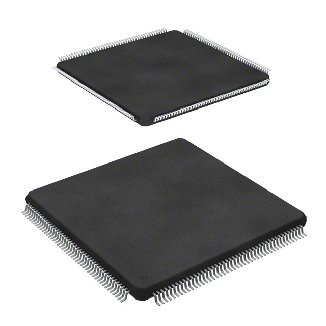
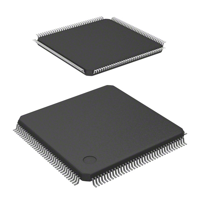
Packaging options and pinout information for STM32L412RBT6P
The STM32L412RBT6P is housed in a 64-pin Low Profile Quad Flat Package (LQFP), a configuration that is widely adopted for projects requiring moderate I/O density and balanced board-level robustness. The LQFP standardizes pin pitch at 0.5 mm, aiding both automated assembly processes and rapid prototyping cycles. The form factor presents significant value for designs targeting footprint-conscious embedded platforms where mechanical clearance and thermal management must co-exist.
Underlying the package choice, the interconnection model is optimized for minimal signal cross-talk, supporting reliable high-frequency operation across both digital and analog domains. Pinout documentation reveals well-structured mappings: Each pin assignment is carefully arranged to minimize adjacency conflicts and signal migration, with power supply pins strategically separated from high-speed digital I/O lines. Analog pins feature proximity to reference and supply nodes, enhancing noise immunity in sensor-driven or data-acquisition circuits.
Alternate function flexibility is a key aspect. The STM32L412RBT6P leverages the STM32 pin multiplexing paradigm, permitting on-the-fly remapping of peripheral interfaces—such as UART, SPI, I2C, timers, and PWM outputs—based on firmware configuration. This agility enables designers to optimize signal routing as board topologies evolve during iterations, supporting either dense peripheral clustering or distributed modular sub-systems. Peripheral routing accommodates advanced PCB trace layouts, including controlled impedance and differential pairs for communication buses.
Supply and reference pin grouping improves power integrity and analog signal acquisition. VDD and VSS pairs are distributed uniformly around the package, reducing voltage drop across the die, while dedicated reference voltages anchor precision ADC and DAC operations. Designers can exploit this topology to segment power domains or reinforce noise boundaries through targeted decoupling, directly benefiting EMC compliance and analog performance.
The package adheres to RoHS and REACH directives, ensuring restriction of hazardous substances throughout manufacturing and distribution. ECOPACK classification further guarantees compatibility with environmentally-conscious procurement practices as component supply chains migrate toward sustainability targets.
Routine layout implementations highlight the practicality of the LQFP format. Workflows often employ ground ring layouts to suppress EMI, and thermal vias beneath the package to manage heat dissipation for sustained high-MCU workloads. Signal routing benefits from corner-exit pin clusters, reducing trace length for timing-critical paths. However, experienced practitioners observe that analog reference pins should be isolated from noisy high-frequency signals, preferably situated at PCB boundaries to optimize SNR in mixed-signal designs.
An essential perspective is the impact of flexible alternate functions on board-level reuse and revision. The architecture supports rapid migration between application profiles—such as shifting from sensor interface to control loop expansion—without costly hardware spin. This aligns with contemporary design philosophies prioritizing adaptability and modularity.
In conclusion, the STM32L412RBT6P’s LQFP packaging and comprehensive pinout schemes serve as a robust baseline for scalable embedded circuitry, merging environmental responsibility with field-oriented practicality. The nuanced interplay between pin function multiplexing, power management, and form factor delivers an optimal canvas for engineering solutions across diverse control, monitoring, and automation contexts.
Potential equivalent/replacement models for STM32L412RBT6P
Selecting functionally equivalent or replacement microcontrollers for the STM32L412RBT6P requires granular evaluation across several technical layers. At the architectural core, devices within the STM32L4 family—specifically, STM32L412CB, STM32L412RB, STM32L411CB, STM32L432KC, and STM32L442KC—share the ARM Cortex-M4 core, delivering comparable computational throughput and DSP capabilities optimized for energy-sensitive embedded applications. These models maintain similar clock configurations and core power management features, sustaining the ultra-low-power operation fundamental to the STM32L412 series.
Peripheral and memory mapping constitute the next critical differentiation. While the core processor remains consistent, each family member introduces variations in embedded flash, SRAM capacity, and available package types. This granularity impacts resource allocation for firmware, alongside PCB layout constraints due to differences in pin count and assignment. For instance, shifting between RB and KC package variants may necessitate signal rerouting on multilayer boards or adjusting part placements to accommodate new I/O locations. In practical migration cases, minor firmware adaptation—such as updating startup files or redefining pin assignments—usually eliminates most barriers to interchangeability if the primary functionality remains within the supported subset.
At the interface and feature integration layer, peripheral set discrepancies become pronounced. Some alternatives offer richer analog front-ends, additional DAC or OPAMP blocks, or expanded communication modules (I2C, SPI, USART). These distinctions necessitate a detailed examination of application requirements, particularly for systems relying on specialized peripherals or low-power analog sensing. In supply chain volatility scenarios, readiness to pivot to alternative STM32L4 family members, supported by up-front abstraction in firmware and PCB design, reduces lead-time exposure while maintaining firmware reusability.
Expanding the equivalence search to STM32L4x5, STM32L4x6, or even STM32L1 series broadens the design flexibility but introduces divergence in power consumption profiles, peripheral granularity, and package availability. Newer subfamilies often bring enhanced features or efficiency improvements at the expense of subtle changes in register maps, startup sequences, or interrupt vectors, which may require deeper firmware adjustments and more comprehensive hardware verification. Notably, STM32L1, built on the Cortex-M3 core, lacks certain M4-specific instructions and DSP extensions, imposing constraints for applications leveraging advanced signal processing.
Experience shows that forward compatibility is most robust when peripheral initialization and hardware signal assignments are modularized from application logic. Pre-silicon hardware abstraction enables more predictable migration even among MCUs with slightly different power domains or wake-up behavior. Integrating conditional compilation and hardware detection routines in the build system further accelerates board bring-up when supply chain dynamics dictate a last-minute component change.
Overall, STM32L412RBT6P alternatives are best selected with a layered approach, beginning from computational core and extending through peripheral mapping to domain-specific features. Carefully staged abstraction within both hardware and firmware frameworks amplifies resilience against part shortages and extends the viable component pool, ensuring both ongoing product maintainability and strategic supply flexibility in dynamic engineering environments.
Conclusion
The STM32L412RBT6P microcontroller presents an optimal equilibrium of energy efficiency and computational resources, grounded in a Cortex-M4 core. The architecture’s low-power design—leveraging dynamic voltage scaling, multiple sleep modes, and fast wakeup—is engineered for battery-dependent applications that demand persistent operation. Integrated analog features such as 12-bit ADCs with low-input leakage and flexible comparators, alongside a diverse digital suite including SPI, I2C, and USART, enable precise measurement and reliable connectivity across industrial and healthcare scenarios. The microcontroller’s flash and SRAM capacities, configurable through standard packages, permit robust firmware management and real-time task execution without memory bottlenecks.
From a system engineering perspective, the hardware security module with AES encryption, true random number generator, and read-out protection directly supports risk mitigation strategies required for medical and industrial protocols. Error correction, brown-out detection, and robust clock supervision ensure operational integrity under fluctuating supply conditions, minimizing downtime and fault incidence in deployed environments. The integrated debugging and programming support—SWD, JTAG, and bootloader options—streamline prototyping phases and field firmware upgrades, reducing time-to-market in iterative development cycles.
Selecting STM32L412RBT6P requires a systematic evaluation of its peripheral breadth against the exact needs of the target application. Practical deployments in sensor nodes have highlighted the chip’s autonomous peripheral operation as a key asset for power-critical routines, where direct memory access and event-driven wakeups preserve battery longevity. The flexible pin mapping and scalable package options simplify hardware revisioning, facilitating upstream and downstream design migration within the STM32L4 family. Engineers must also weigh supply chain considerations, such as component lifecycle and vendor assurance, for long-term reliability in regulated sectors.
Current adoption trends indicate the STM32L412RBT6P is well-positioned at the intersection of energy-constrained devices and feature-rich control subsystems. Its versatility extends the foundational applicability of the STM32L4 platform, particularly when projects require seamless integration of security, low-power operation, and analog precision. Strategic deployment of this microcontroller unlocks differentiated capabilities in system architectures—supporting both immediate solution requirements and scalable future enhancements.