 >
>


Product Overview: STM32F412RGY6TR Microcontroller
The STM32F412RGY6TR microcontroller, part of STMicroelectronics’ STM32F4 series, exemplifies optimized integration of computing resources for embedded system design. Its foundation is the ARM Cortex-M4 core, which leverages a 32-bit architecture and operates at frequencies up to 100 MHz. This processing engine supports DSP instructions and a single-precision floating-point unit, enabling efficient execution of complex mathematical algorithms, such as digital filtering, sensor fusion, and control loop routines within time-critical industrial and consumer applications.
On-chip memory is provisioned with 1 MB of flash and 256 KB of SRAM, facilitating sophisticated code structures, multi-buffered communication stacks, and real-time data logging without external components. This capacity, in relation to die size constraints, supports advanced firmware storage, bootloader architecture, and memory-resident application layers. Flash endurance and retention characteristics ensure reliability across repeated update cycles, an essential consideration in field-upgradable systems and remote device management frameworks.
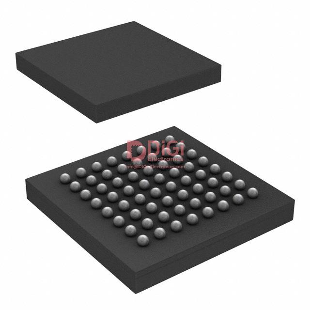
The microcontroller, encapsulated in a 64-WLCSP package measuring 3.62 x 3.65 mm, achieves minimal footprint for streamlined PCB layouts. This package selection allows high-density designs, where routing and signal integrity may pose challenges; strategic layer stacking and careful power domain partitioning become essential for mitigating cross-talk and ensuring thermal stability. Such compactness directly benefits wearables, IoT edge nodes, and instrumentation modules, where volumetric efficiency must not compromise core performance or peripheral accessibility.
Peripheral integration is engineered for versatile connectivity: high-speed SPI, UART, I2C, multiple timers supporting PWM, advanced ADCs, and flexible GPIO assignments equip this device for sensor interfacing, actuator control, and multi-protocol communications. The microcontroller’s clock management and power control subsystems further contribute to ultra-low-power operation, with flexible standby and sleep modes that support battery-run deployments and energy-harvesting platforms. In practice, careful dynamic switching between low-power states and active execution, governed by real-time workload profiling, delivers extended operational autonomy in field devices.
System-level reliability benefits from the STM32F4 family’s embedded safety features, such as fault-tolerant reset domains, clock watchdogs, and high-precision brownout detectors. These mechanisms provide predictable recovery from transient faults and guarantee consistent behavior under variable environmental conditions. The device further supports secure boot patterns and hardware-backed code protection, critical for maintaining firmware integrity and safeguarding intellectual property in connected systems.
Engineering teams routinely exploit the STM32 ecosystem’s software toolchains—HAL/LL drivers, middleware stacks, and real-time operating systems—which align closely with device hardware to accelerate prototyping, certification, and scaling. When configuring resource allocation, practical experience prioritizes peripheral multiplexing, DMA optimization, and event-driven interrupt structures, maximizing throughput while minimizing latency. Layered abstraction permits modular code reuse and platform scalability, supporting both minimalistic single-task firmware and complex multitasking audio or motor control architectures.
Selecting the STM32F412RGY6TR represents a balance between computational density, low power consumption, and connectivity breadth—attributes that converge to fulfill diverse application scenarios in medical instrumentation, robotics, smart sensors, and portable analytics. This equilibrium underscores a core insight: advanced microcontroller solutions must harmonize raw processing power with efficient resource management, secure interfacing, and adaptability to emerging system architectures.
Core Architecture and Performance of STM32F412RGY6TR
The STM32F412RGY6TR is architected around the ARM Cortex-M4 processor, integrating a floating point unit (FPU) essential for high-speed digital signal processing and precision arithmetic. This core is tailored to handle computationally intensive control tasks, where both integer and floating-point calculations are frequent requirements. The ARMv7-M instruction set, along with advanced DSP extensions, forms the computational backbone, enabling efficient manipulation of signal data structures and real-time control loops. The presence of the FPU considerably reduces computation latency in applications such as motor control, audio filtering, and sensor fusion.
Performance is further enhanced by the embedded ART (Adaptive Real-Time) accelerator. This subsystem orchestrates flash memory transactions through an intelligent prefetch and cache mechanism, maintaining zero-wait state read conditions even during sequential code execution. As a result, the processor sustains maximum throughput at up to 125 DMIPS, ensuring responsiveness in cycles where high data bandwidth and low latency are critical—such as in control systems, digital filters, and feedback loops. The near-instantaneous code fetch directly from the flash enables a compact yet high-performing system design, minimizing bottlenecks normally associated with embedded non-volatile memory access.
Security and reliability mechanisms play a pivotal role in the STM32F412RGY6TR architecture. A dedicated memory protection unit (MPU) enforces access boundaries within the memory map, preventing errant code from corrupting sensitive regions and supporting robust partitioning in multi-tasked firmware environments. This feature is vital in systems where isolation between communication stacks, application code, and bootloaders is non-negotiable for integrity and resilience. Additionally, the on-chip CRC calculation unit accelerates integrity verification operations, streamlining safety-critical routines for firmware updates, data transmission, and runtime health checks.
From a practical perspective, leveraging the DSP instruction set in conjunction with the FPU has shown considerable improvement in execution times for algorithms requiring fast Fourier transforms or PID control. Consider, for instance, filtering sensor data in industrial automation: the processor’s combined instruction set and optimized memory access translate directly to faster loop cycles and reduced jitter, enabling deterministic behavior in time-sensitive applications. The ART accelerator’s impact becomes evident when continuous code streams are executed without performance drops, supporting seamless control in applications where timing errors could lead to system instability.
An insightful takeaway can be drawn from the tight integration of these architectural elements. The synergistic relationship between the real-time accelerator, memory protection, and DSP-fused core contributes not only to raw performance but also to enhanced robustness of embedded systems. This design philosophy allows for firmware architectures that confidently scale both computational intensity and security requirements, advancing capabilities in fields as diverse as automation, smart instrumentation, and secure IoT nodes.
Integrated Memory and Data Handling Features in STM32F412RGY6TR
STM32F412RGY6TR integrates a robust internal memory architecture, which is foundational for embedded systems requiring both large code footprints and responsive data management. The 1 MB flash enables deployment of sophisticated firmware, fully accommodating features such as advanced protocol stacks or embedded GUIs. The 256 KB SRAM offers ample space for multi-buffered data, large working arrays, and dynamic allocations, ensuring real-time operations remain uninterrupted even under memory-heavy workloads. Efficient execution is further enhanced by hardware mechanisms supporting zero-wait-state access, contingent on clock configuration and code placement.
External memory interfacing is addressed through the Flexible Static Memory Controller (FSMC), allowing seamless connectivity to a variety of memories—SRAM, NOR, PSRAM—via configurable up-to-16-bit data buses. These lines support high-throughput data exchanges, optimizing boot processes and storage of dynamic or bulk data. Hardware engineers find value in the FSMC’s timing programmability, which is critical when negotiating compatibility with diverse off-chip memories. In particular, the controller’s automated management of multiplexed address/data signals circumvents race conditions common during initialization phases, offering durable reliability for designs expected to operate in variable environments.
The batch acquisition mode (BAM) presents a curated solution for power-sensitive applications needing periodic sampling or event-driven data capture. BAM autonomously collects sensor or peripheral input into memory segments, minimizing CPU intervention and gating consumption—especially vital in battery-operated nodes. Practical deployments often leverage BAM in conjunction with DMA, forming pipelines that decouple acquisition logic from high-level event processing. This orchestration reduces latency, ensures data integrity, and preserves precious MCU cycles for top-level control tasks.
Central to overall throughput is the multi-AHB bus matrix, which orchestrates concurrent access pathways among the core, memories, and peripherals. This multi-layer architecture prevents bottlenecks and priority inversion during simultaneous operations, such as audio streaming, graphics rendering, and protocol handling. The bus matrix’s dynamic arbitration enables deterministic latency, crucial for systems with real-time deadlines and heavy transaction loads. Designers optimizing for scatter-gather or multi-threaded protocols find the bus matrix’s isolation capabilities instrumental in maintaining low-jitter data paths.
Alongside, the 16-stream DMA controller scales the effective bandwidth across peripherals and memory domains. Its versatility—spanning circular buffering, memory-to-peripheral, and memory-to-memory transfers—underpins sophisticated data management strategies. Field experience confirms that offloading these data flows from the CPU accelerates ISR response, supports seamless I/O without handshaking overhead, and mitigates throughput spikes that might otherwise stall time-critical algorithms. Precise channel configuration and burst settings are frequently exploited in sensor fusion, video frame capture, and bulk communication interfaces.
Designing embedded solutions with the STM32F412RGY6TR, leveraging its memory and data handling subsystems, allows architecting both resilient and scalable systems with optimal balance between speed, power, and integration. Setups demanding deterministic performance under fluctuating loads benefit from proactive partitioning of memory and DMA resources, alongside explicit priority assignment within bus arbitration. This approach not only preserves functional correctness but elevates system responsiveness, a subtle yet critical distinction in embedded engineering. Integration of internal and external memory with parallel data channels thus forms the backbone of robust, future-proof applications poised for rapid iteration and deployment across varied domains.
STM32F412RGY6TR Connectivity and Peripheral Options
The STM32F412RGY6TR exemplifies advanced integration for connectivity-centric designs, blending a rich set of peripheral interfaces with robust signal handling and analog capabilities. At the core, its architecture delivers seamless data exchange through up to 17 dedicated communication interfaces. These span four I²C ports compliant with PMBus/SMBus standards, ensuring compatibility for power management and system monitoring networks. The inclusion of four USARTs with protocol extensions (LIN, IrDA, ISO 7816) optimizes the device for both legacy and modern serial communications, crucial for mixed-protocol environments prevalent in automotive and industrial automation.
SPI and I²S functions are implemented with uncommon flexibility; five instances accommodate high-bandwidth synchronous data flows, while dual full-duplex I²S channels address demanding real-time audio streaming or low-latency sensor hubs. The hardware CAN 2.0B controller serves low-level deterministic networking, a linchpin for distributed control systems. Two expansion slots for SDIO, MMC, and eMMC permit direct attachment of mass storage modules, offloading critical tasks from the MCU core during large data transfers or firmware updates.
USB 2.0 FS with native OTG (On-The-Go) transitions the role of the microcontroller between host and device, supporting applications from field firmware updates via flash drives to temporary data aggregation endpoints. The Quad-SPI interface stands out for high throughput connectivity to external serial flash, streamlining execution-in-place (XiP) code architectures and accelerating resource-intensive boot or graphics code fetching.
Up to 114 general-purpose I/O pins feature high voltage tolerance and rapid switching—providing deterministic, low-latency control, and multi-level logic compatibility essential for interface bridging and real-world signal acquisition. Pin multiplexing minimizes board complexity, allowing dense integration of peripheral modules without routing congestion. The GPIOs also support direct interrupt triggering on rising, falling, or both edges, crucial for rapid response in time-sensitive control loops.
Analog processing leverages a high-speed, 12-bit ADC, sampling at up to 2.4 MSPS across 16 multiplexed channels. This supports parallel acquisition of multi-sensor arrays or high-fidelity waveform capture, feeding real-time analytics or closed-loop regulation. The integrated sigma-delta modulator and digital filters facilitate isolated measurement paths, enabling robust signal integrity for mixed-signal applications such as precision metrology or sensor fusion.
Deploying this microcontroller leads to streamlined board layouts and reduced BOM count, as most connectivity tasks can be handled in silicon without supplementary logic or bridges. In high-density designs like industrial controllers, instrumentation, or compact gateways, this translates into heightened reliability, simplified firmware architecture, and faster time-to-market. Experience has shown that leveraging flexible peripheral remapping and DMA-driven data transfers unlocks significant headroom both in CPU load and determinism, particularly when orchestrating concurrent communication streams such as CAN-based telemetry with simultaneous USB updates.
The STM32F412RGY6TR’s design favors projects requiring rapid adaptation to shifting interface standards. Its architectural decisions—especially the coexistence of high-speed memory, deterministic networking, and flexible analog front-ends—reveal a clear intent to anchor connectivity-driven embedded solutions. This platform not only reduces integration risk but also catalyzes innovation in edge-compute and real-time data acquisition scenarios.
Power Management and Low-Power Modes in STM32F412RGY6TR
Power management in the STM32F412RGY6TR is architected to maximize both operational versatility and energy efficiency, leveraging a wide supply range from 1.7 V to 3.6 V for robust adaptation across varied hardware ecosystems. This voltage range supports dynamic scaling, empowering design optimization for both high-performance and ultra-low-power deployments.
The microcontroller integrates granular low-power modes—Sleep, Stop, Standby, and VBAT—each with unique current profiles and context retention capabilities. Sleep mode suspends the CPU while peripheral clocks remain active, useful for applications requiring rapid periodic wake-ups with modest consumption. Stop mode leverages oscillator gating and RAM retention, balancing state preservation with deep current savings. Standby mode executes more aggressive power gating, disconnecting internal voltage regulators and losing most system context while maintaining backup domain and tamper detection. VBAT mode further isolates the MCU to focus exclusively on the RTC and a handful of critical registers, minimizing quiescent draw for long-duration battery shelf life.
Transition dynamics between these modes—including sub-millisecond wakeup on Stop and Standby—enable implementation of power gating techniques without noticeably impacting responsiveness. Real-time clock precision remains uncompromised even in deep sleep, satisfying requirements for time-critical maintenance cycles and scheduled events in systems such as remote sensors or wearable instrumentation.
Supply integrity is maintained by embedded reset and voltage monitoring mechanisms. These oversee regulator margins and peripheral voltage rails, imposing event-driven resets to shield against erratic supply fluctuations or brownouts. Sophisticated configuration options for threshold and response timing allow tailored protection policies, improving system reliability in electrically challenging environments.
Successful power management hinges on careful profiling of workload, external IRQ sources, and retention needs. Experience demonstrates that user-defined wakeup sources, such as external pins or internal timers, must be provisioned to balance energy savings against necessary latency metrics. Reliable RTC operation in VBAT mode is achievable with meticulous clock calibration against environmental drift factors and battery quality. Custom regulator options and adaptive reset thresholds optimize fault tolerance, particularly in mixed-supply environments subject to transient injections.
Effective design with the STM32F412RGY6TR leverages multi-layered power schemes, matching operational profiles to current demands and latency constraints. The device’s capabilities support sophisticated energy-saving topologies, combining flexible hardware mechanisms and resilient supervisory layers to achieve high system reliability in low-power and battery-centric applications. Selecting appropriate modes, calibrating retention policies, and tuning supervisory parameters together form the foundation for robust embedded power solutions.
Package Details and Mounting Considerations for STM32F412RGY6TR
The STM32F412RGY6TR is housed in a compact 64-WLCSP (Wafer Level Chip Scale Package), enabling high functional density within a footprint of 3.62 x 3.65 mm. Such a form factor directly supports aggressive miniaturization targets in wearable electronics, ultra-mobile platforms, and space-constrained IoT modules. Design flexibility emerges from systematic allocation of power, ground, and IO pads, which not only simplifies multilayer PCB routing but also fosters optimal signal integrity by reducing parasitic effects commonly associated with high-density layouts.
Underlying the package design are robust thermal and electrical controls. The die-to-board thermal path leverages the large exposed copper planes beneath critical pads, facilitating efficient heat dissipation even at peak loads within the specified -40°C to +85°C operating envelope. Implementing a dedicated ground plane under the device, coupled with low-impedance vias arranged in a regular array, helps maintain low noise margins. Empirical results show that careful regulation of solder volume during reflow—ensuring full paste stencil coverage across the ball grid—enhances joint reliability and reduces the risk of thermal cycling fatigue.
Surface-mount considerations extend to handling the WLCSP's sensitive interface; for example, footprint design benefits from symmetric pad arrangement and optimized via-in-pad techniques to minimize solder wicking and maximize mechanical stability. Applying X-ray inspection post-reflow confirms ball connectivity and detects voids with high granularity, accelerating yield assessment. In practical deployment for industrial sensors, integrating local decoupling capacitance adjacent to power paddings improves immunity to transient load spikes, directly supporting stable operation under stochastic workloads.
Intrinsic to successful integration is the recognition that such high-density packaging demands tightly controlled reflow profiles and substrate flatness to avoid warping, which can lead to intermittent IO performance. Interfacing with fine-pitch BGA layouts at this scale requires calibrated pick-and-place procedures and active monitoring of placement pressure, which have proven to reduce instances of micro-cracking in fragile substrate regions.
In summary, the STM32F412RGY6TR's 64-WLCSP package exemplifies progressive miniaturization and integration efficiency. Its proven mechanical and electrical optimizations, when paired with disciplined board-level design practices, unlock substantial reliability and manufacturability gains in advanced embedded computing platforms.
Environmental Ratings and Compliance for STM32F412RGY6TR
Environmental ratings and compliance for STM32F412RGY6TR are anchored in well-defined regulatory frameworks and chip-level engineering controls. The device fully adheres to RoHS3 directives, prohibiting the use of hazardous substances in electrical and electronic equipment, and is classified as REACH unaffected, indicating that none of its constituents fall under the stringent candidate list for substances of very high concern. This baseline aligns the component with global market entry requirements and reduces risk for application in ISO 14001-driven supply chains.
A critical metric for operational reliability, the device's Moisture Sensitivity Level (MSL) of 1 signals unlimited floor life at ≤30°C/85% RH. This directly benefits volume manufacturing by eliminating staging constraints and mitigating latent field failures associated with popcorning during reflow. Production lines thus gain flexibility, particularly important in just-in-time environments and when rapid design iterations demand agile assembly schedules. This attribute also simplifies logistics, where components may circulate through multiple contract assembly partners before final product integration.
The inclusion of a unique 96-bit hardware identifier offers hardware-level traceability, integrating seamlessly with inventory management, quality assurance, and anti-counterfeiting strategies. This trace mechanism is especially effective in sectors such as medical and industrial automation, where regulatory audits and recalls demand pinpoint provenance. The practical upshot is shorter disposition cycles and greater granularity in root-cause failure analysis when systemic defects surface.
ECOPACK2 package compliance represents the intersection of regulatory discipline and material innovation, certifying that the STM32F412RGY6TR packaging meets advanced restrictions on environmentally harmful substances and supports recyclability. This results in a lower environmental footprint in the supply chain and aids end-of-life product stewardship, benefitting design-to-disposal strategies now standard in product lifecycle management.
Electromagnetic compatibility and electrostatic discharge protection encapsulate the device’s resilience in real-world deployments. The STM32F412RGY6TR supports extensive EMC and ESD requirements, leveraging internal design safeguards and silicon process controls. In practice, this routinely translates to robust performance in electrically noisy environments—industrial control, laboratory instrumentation, and portable medical analyzers—where transient immunity and low spurious emissions are non-negotiable. Such capabilities simplify system-level compliance with CE and FDA standards, reducing the need for heavy external filtering and iterative shielding modifications.
Engineering selections based on this device can thus reliably address sustainability mandates while minimizing compliance-induced redesign cycles. By integrating environmentally compliant design with practical reliability and traceability features, the STM32F412RGY6TR exemplifies a balanced approach where regulatory and technical risk are both managed at the silicon level—a distinctive advantage in fragmented and safety-critical markets.
Application Scenarios for STM32F412RGY6TR
The STM32F412RGY6TR microcontroller presents a sophisticated blend of high-speed processing, advanced communication capabilities, and flexible analog-digital integration, positioning it as a versatile cornerstone in embedded system development across various application domains. Its architecture, based on an ARM Cortex-M4 core with Floating Point Unit (FPU), underpins deterministic real-time computation demanded by tightly-coupled control loops and signal processing algorithms. The multifaceted peripheral suite—encompassing DMA controllers, hardware crypto engines, extensive timer options, and synchronized ADC/DAC channels—enables the design of complex, responsive, and secure embedded modules.
In industrial automation, the STM32F412RGY6TR addresses the nuanced requirements of programmable logic controllers (PLCs), variable-frequency inverters, and digital circuit breakers. Its real-time capabilities harmonize precise sensor fusion and actuator control, minimizing latency in fault detection and protective switching while maintaining system stability under electromagnetic interference. The integrated hardware encryption modules streamline secure communication and firmware authentication, critical where sabotage or data manipulation risks are present. Deploying the STM32F412RGY6TR in a modular PLC backplane demonstrates its resilience to harsh electrical environments, while the fine-grained power management features maintain operational integrity during transient load conditions.
For medical instrumentation, the low-noise analog front-ends and high-resolution ADCs enable trustworthy bio-signal acquisition and post-processing—crucial for patient monitoring, diagnostic imaging, or handheld diagnostic equipment. The tightly-coupled DMA and digital filter blocks offload resource-intensive tasks from the core, allowing consistent real-time operation for sensor calibration, waveform analysis, and anomaly detection routines, even as the device handles encrypted wireless data exchange with medical records infrastructure.
Precision motor drives in industrial robotics and automation leverage the microcontroller’s advanced timer synchronization and high-frequency PWM outputs. These resources translate to sub-millisecond control granularity, yielding accurate speed and torque regulation for brushless motors. Rapid interrupt response coupled with fault-tolerant features assures safe operation under dynamic electrical and mechanical strain—a direct advantage in redundant safety-system architectures.
In consumer domains, the STM32F412RGY6TR’s flexible digital audio interfaces and on-chip DSP instructions make it suitable for high-fidelity home audio systems and active noise-cancellation applications. The robust serial and parallel interface support facilitates seamless integration with Bluetooth modules, WiFi SoCs, and MEMS microphones, expanding smart home and wearable device functionality. Deploying it as a sensor hub in mobile or wearable products highlights its efficiency in aggregating and preprocessing multi-modal sensor data, efficiently balancing performance with battery life using dynamic frequency scaling and low-power sleep modes.
Within the IoT ecosystem, built-in security primitives ensure end-to-end device authentication and encrypted telemetry, essential as edge devices proliferate. The microcontroller’s scalable interface options—from SPI and I2C through high-speed USB OTG—enable native integration of diverse wireless modules and sensor arrays, future-proofing designs against evolving connectivity standards. Its flexible boot and update mechanisms further support robust over-the-air firmware updates critical to secure, long-lived field deployments.
Integrating the STM32F412RGY6TR in these scenarios reveals that its true utility emerges not merely from hardware specifications, but from the cohesive interplay of deterministic processing, flexible interfacing, and embedded security. These traits accelerate time-to-market for advanced edge devices while enabling confident deployment in safety- and mission-critical environments—a convergence that aligns with the rapidly evolving demands of modern embedded engineering.
Potential Equivalent/Replacement Models for STM32F412RGY6TR
Understanding the migration landscape within the STM32F412 series requires a structured approach grounded in the device’s architecture, peripheral mapping, and memory organization. At the foundational level, these microcontrollers share a consistent core architecture based on the ARM Cortex-M4, maintaining compatibility in firmware development and support for DSP instructions and floating point unit operations. The primary differentiators hinge on memory size (Flash and SRAM), IO capacity, and package type, necessitating a granular assessment of system requirements before substituting components.
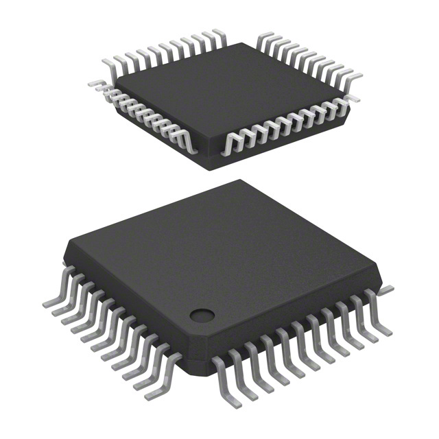
Pinout congruence across STM32F412RE, F412VE, F412ZE, F412CG, F412RG, F412VG, and F412ZG ensures minimal disruption when exchanging parts, provided the selected device aligns with the existing PCB topology. The mutual availability of features—such as multiple SPI, I2C, UART interfaces, advanced timers, and integrated USB OTG—reinforces software portability, while differences in peripheral count and RAM/Flash allocations demand careful correlational analysis. Assessing these distinctions along with voltage, oscillator, and package attributes (LQFP, UFBGA, UFQFPN) mitigates downstream issues during prototyping and mass production.
Application engineers often prioritize pin compatibility to streamline layout reuse and accelerate development. However, subtle discrepancies in available functional blocks can surface—such as differential ADC channels or variations in DMA streams—creating downstream implications in applications with strict real-time or signal processing constraints. For instance, migrating from the STM32F412RGY6TR to the STM32F412ZE may provide expanded memory and IO, but necessitates validation of timing performance and resource allocation, particularly in sensor fusion or industrial control applications.
Practical selection also involves consideration of long-term availability and supply chain resilience, with broader package options (e.g., 100 to 144 pins) providing flexibility if alternate assembly vendors or assembly constraints arise. Pin-compatible options support test coverage simplification and reduce NPI risk. In scenarios where footprint minimization is critical, smaller packages like UFQFPN may be preferable, albeit with potential sacrifices in peripheral count.
Informed device selection balances physical and logical compatibility with cost, lifecycle support, and performance margins. When evaluating substitutes for STM32F412RGY6TR, prioritizing modularity and firmware abstraction ensures the embedded system remains extensible and maintainable, thereby future-proofing the design against ongoing component shifts and market dynamics. Consistent peripheral and core behavior across the STM32F412xE/G series allows for controlled scalability, underpinning robust embedded solutions in industrial control, consumer electronics, and connected IoT devices.
Conclusion
The STM32F412RGY6TR microcontroller demonstrates a compelling balance of computational performance, integration density, and system-level versatility. At its core, the device utilizes an ARM Cortex-M4 processor with Floating Point Unit, enabling efficient execution of both integer and signal processing algorithms—critical for real-time control and embedded DSP workloads. This architecture supports deterministic interrupt handling and robust throughput, both essential for time-sensitive industrial automation, precision instrumentation, and advanced user interfaces.
A notable strength of the STM32F412RGY6TR lies in its comprehensive connectivity matrix. Equipped with high-speed SPI, I2C, USART, USB OTG, and SDIO peripherals, the device streamlines integration with a broad array of sensors, actuators, and communication modules. This design flexibility facilitates modular system topologies, accommodating evolving I/O requirements without substantial redesign. The embedded Direct Memory Access (DMA) engine further optimizes peripheral interactions by offloading data transfer tasks, safeguarding CPU bandwidth for mission-critical computations—an advantage that becomes apparent in multi-channel acquisition and data-logging scenarios.
Data management is enhanced through a rich assortment of SRAM and Flash, supporting dynamic resource allocation and firmware over-the-air upgrades with minimal disruption. The integrated cryptographic accelerators and True Random Number Generator provide the foundation for secure data exchange, which proves indispensable in medical devices and connected industrial platforms where infection points for cyber threats persist.
In energy-sensitive deployments, the STM32F412RGY6TR’s extensive power management features—including multi-level clock gating, dynamic voltage scaling, and deeply integrated sleep modes—allow for precise calibration of power consumption. This quality is directly observable in battery-operated field instruments, where operational endurance and quick wake-up responses are required.
Package availability in UFQFPN and WLCSP variants enhances mechanical adaptability, supporting both footprint-constrained wearables and densely packed control boards. The device’s pinout compatibility across the STM32F4 Series fosters design reuse and expedites platform upgrades, an approach that underpins scalable product families.
From a deployment perspective, mature hardware abstraction layers and development ecosystem yield short design cycles and rapid prototyping advantages, lowering total engineering overhead. Debugging and trace features reduce time-to-diagnosis in field reliability efforts, an often-overlooked lever for sustained product quality as system complexity grows.
It is evident that the STM32F412RGY6TR’s combination of real-time processing capability, energy efficiency, and ecosystem maturity sets a high standard for embedded controllers tackling multi-domain challenges in industrial, medical, and consumer environments. The subtle symbiosis between hardware scalability and software support enables not only current applications but also agile adaptation to future technical demands, anchoring next-generation embedded platform strategies.