>
>


Product overview: STM32F378VCT6 and STM32F3 series
Product overview: STM32F378VCT6 and STM32F3 series. The STM32F378VCT6 microcontroller is a member of STMicroelectronics’ STM32F3 series, targeting applications requiring robust mixed-signal integration and efficient processing. It is built around an ARM Cortex-M4F core with DSP and floating-point capabilities, operating up to 72 MHz. The STM32F378VCT6 offers a rich blend of analog and digital peripherals combined with 256 KB of embedded Flash and 32 KB SRAM, and is housed in a 100-pin LQFP package (14 x 14 mm). This device meets demanding requirements in industrial automation, instrumentation, motor control, and precision sensing scenarios.
Upgraded and Expanded Content:
The STM32F378VCT6, as part of the STM32F3 series, embodies a well-balanced architecture tailored for mixed-signal control applications. Central to its design is the ARM Cortex-M4F core, which merges a single-cycle multiply-accumulate unit with hardware-accelerated floating-point support. This configuration enables the device to perform computationally intensive signal processing operations, such as digital filtering and real-time control algorithms, without offloading tasks to external processors. The 72 MHz clock speed, combined with an efficient interrupt and execution pipeline, ensures low-latency response times vital for embedded control systems.
Integrated analog peripherals stand out in the STM32F378VCT6, distinguishing it from many general-purpose microcontrollers. The device features fast, high-resolution ADCs, multiple DAC channels, comparators, and programmable operational amplifiers. These peripherals support both simultaneous sampling and complex analog front-end design, supporting high-precision measurement in closed-loop control systems and instrumentation. This tight coupling of analog functions with the main processing core significantly reduces system complexity, PCB footprint, and BOM cost, especially in applications like three-phase motor drive or industrial sensor nodes.
Embedded memory resources are well-aligned with typical application requirements. The 256 KB Flash provides sufficient space for application firmware with modular updates, while the 32 KB SRAM allows for robust support of real-time data buffers, lookup tables, and stack-intensive signal-processing routines. On-chip memory, with execution-in-place (XiP) capabilities, minimizes bus contention, enabling deterministic execution—a factor directly impacting system reliability in mission-critical deployments.
In terms of I/O and connectivity, the 100-pin LQFP package offers significant pin availability, facilitating extensive peripheral mapping. Flexible remapping of timers, UARTs, SPIs, and I2C channels enhances design scalability and simplifies board layout. Advanced PWM generation and fast timer capture/compare channels suit dynamic motor control and precision actuation tasks. Multiple communication interfaces streamline device integration into industrial fieldbuses or sensor networks, enabling both centralized and distributed architectures.
From a system-level engineering perspective, deploying the STM32F378VCT6 often leads to reduced development cycles. Well-documented reference designs and robust software libraries, such as the STM32CubeF3 HAL/LL drivers, accelerate prototyping of DSP tasks, analog acquisition, or closed-loop control. Developers typically note consistent ADC calibration routines, reliable interrupt handling for event-driven designs, and effective use of hardware-assisted floating-point for application-layer computations. A unified development toolchain—encompassing simulation, debugging, and in-circuit programming—further optimizes workflow, especially when migrating from earlier STM32 devices or scaling to different package variants within the F3 series.
Architecturally, the STM32F378VCT6 occupies a unique position where analog density, real-time response, and digital signal processing capability intersect. This allows for direct implementation of algorithms such as PID, Clarke/Park transforms, and sensor fusion within a single chip, without two-tiered microprocessor-microcontroller partitioning. The device effectively bridges gaps between pure MCU solutions and more complex mixed-signal SoCs, offering a robust engineering platform for evolving requirements in industrial, automotive, and instrumentation sectors.
Key architectural features of the STM32F378VCT6
The STM32F378VCT6 leverages an ARM Cortex-M4F core, which forms the backbone of its computational capabilities. This processor integrates single-cycle multiplication and division units, enabling high-throughput arithmetic required for time-sensitive signal processing and control algorithms. Of particular importance is the inclusion of DSP-oriented instructions and a dedicated floating-point unit, facilitating efficient execution of complex mathematical operations. The architecture consistently achieves up to 1.25 DMIPS per MHz, empowering developers to implement demanding real-time routines without incurring significant latency.
Memory protection mechanisms are baked into the design via the integrated MPU, crucial for segmenting execution domains and preventing inadvertent memory access errors. This feature supports embedded software reliability, particularly in multi-threaded environments or safety-critical applications. The external power-on reset logic is structured to ensure stable initialization under varying supply conditions. This mechanism mitigates common startup issues, such as spurious boot events, thus promoting consistent system behavior in diverse deployment scenarios.
Reliability at the system level is further reinforced by hardware components dedicated to fault detection and response. The embedded cyclic redundancy check unit can be harnessed for runtime data integrity verification, notably in firmware validation and communication protocols. Coupled with the NVIC interrupt controller, the architecture delivers deterministic and prioritized event handling across multiple I/O sources. Configuring interrupt priorities judiciously has proven valuable in practical deployments requiring responsive motor control or sensor interfacing, where timing margins are tight.
By interlocking rapid arithmetic, signal processing acceleration, robust memory protection, and deliberate startup management, the STM32F378VCT6 provides a cohesive framework for high-integrity real-time systems. The interplay between these architectural elements supports both innovation and operational predictability, especially when deployed in industrial automation and instrumentation tasks. The combination of hardware-backed reliability and computational efficiency distinguishes this microcontroller, presenting critical advantages over less integrated alternatives in embedded product engineering.
Memory subsystem details in STM32F378VCT6
The STM32F378VCT6 leverages a finely tuned memory subsystem engineered for embedded applications demanding reliability, deterministic response, and code efficiency. The 256 KB embedded Flash is mapped for zero-wait-state execution at typical system frequencies, supporting robust in-place code execution and facilitating frequent in-field firmware upgrades thanks to sector-based erasure and fast programming algorithms. This non-volatile storage aligns with the need for secure, long-term retention of critical program code and bootloader routines, often exploited in systems requiring remote updates or protected firmware zones. Code density optimizations such as Thumb-2 instruction set support further enhance available space for application logic within the Flash footprint.
Complementing Flash, the 32 KB SRAM, protected via hardware parity checking, serves as the primary working memory for stack, heap, and real-time buffering. Parity error detection acts as an immediate safeguard against bit-flip incidents, especially crucial in electromagnetic interference-prone environments or mission-critical control loops. The tight coupling between the core and SRAM, together with deterministic access, enables fast context switching, deterministic interrupt response, and efficient block I/O operations—properties especially valued in motor control, digital power conversion, and time-sensitive sensor acquisition routines. This memory area typically divides into fast-access buffers, communication rings, and control parameters, with developers often segmenting regions for DMA coherence or zero-initialization at boot.
DMA (Direct Memory Access) architecture featuring 12 independent channels allows offloading repetitive or bulk memory transfers while minimizing CPU intervention. For example, high-throughput peripherals such as ADCs, UARTs, or SPI modules leverage DMA to stream data into SRAM buffers in real time. Applications benefit from significant reduction in interrupt overhead and deterministic data capture windows, essential for waveform acquisition, industrial communication protocols, and high-speed data logging. Segregating DMA-accessible SRAM regions avoids data contention and maximizes throughput, underlining the importance of a nuanced memory partitioning strategy.
Peripheral registers are seamlessly mapped into the memory space, supporting direct, low-latency access from both the CPU and DMA without indirection or translation. This design accelerates control loop cycles and enables predictable register manipulation for precision timing requirements. The flexible remapping configuration accessible at boot allows rapid system customization, such as selecting different startup routines or activating custom firmware images—an approach that lends itself to fault-resilient bootloaders and secure dual-bank code update schemes.
A critical yet often underutilized subsystem is the 128-byte battery-backed backup register domain. This non-volatile memory segment preserves crucial calibration constants, system state variables, or secure authentication tokens across power cycles and resets. In practice, this enables construction of datalogging features with guaranteed retention, power-fail-safe parameter storage, or tamper-resistant timestamp applications. Proper access sequencing and data integrity checks are best practices to maximize reliability and endurance of this limited, yet strategic, storage.
A balanced memory subsystem in the STM32F378VCT6 provides not only speed and storage but also operational resilience and architectural flexibility. Identifying optimal partitioning schemes based on actual application patterns, leveraging hardware error detection prudently, and architecting Direct Memory Access pathways for maximal offload constitute the core of effective embedded software development on this platform. In advanced projects, subtle tuning of Flash sector usage, SRAM layout for DMA coherency, and layered use of backup registers can yield measurable gains in system reliability and throughput—a perspective that moves beyond surface-level datasheet reading toward exploitation of the full potential inherent in the microcontroller’s memory subsystem.
Power supply and low-power management in STM32F378VCT6
Power supply design in the STM32F378VCT6 centers on precision-controlled voltage domains, accommodating diverse operational demands. The VDD provides 1.8 V within an ±8% margin, supporting digital core activities, while VDDA spans from 1.65 V to 3.6 V, powering analog circuitry and ADCs. This tiered voltage provisioning, combined with physically separate pinouts, ensures robust noise immunity. Effective analog-digital isolation greatly enhances signal fidelity in applications such as motor control, instrumentation, and metering, where transient noise can critically degrade measurement reliability.
Low-power operation leverages two well-defined modes: Sleep and Stop. Sleep mode suspends only CPU execution, maintaining full functionality for all peripherals, interrupt controllers, and communication interfaces. This facilitates real-time responsiveness with minimal wake latency, ideal for protocol-driven workflows or constant background sensing. Stop mode, by contrast, reduces system consumption to the sub-milliamp range by powering down clocks and high-frequency domains, preserving only SRAM and register context. Key experience highlights include the careful selection of clocks and IO retention settings within Stop mode, which significantly impact both static current draw and recovery timing. Robust application performance often hinges on balancing SRAM retention depth against clock gating granularity.
Wakeup strategies exhibit substantial flexibility. External events such as pin state changes or dedicated low-power timers can initiate rapid exit from Stop mode, supported by on-chip peripherals with autonomous operation capability. This multimodal wakeup design serves time-critical scenarios—for instance, instant recovery upon external trigger or scheduled interval, essential in sensor networks or portable data loggers. Fine-tuning debounce intervals and prioritizing interrupt sources play decisive roles in minimizing spurious wakeups and optimizing energy budgeting.
Successful deployment in the field reveals that carefully managed VDDA filtering, alongside granular clock gating, pushes operational endurance in battery-powered applications far beyond datasheet estimates. Highlighting this, power profiling during erratic load conditions indicates that analog noise spikes are best mitigated through isolated PCB routing and localized decoupling tied directly to VDDA, rather than global measures. There is distinct value in tailoring power domain sequencing and retention logic to the unique transients of the target application, rather than relying exclusively on default startup profiles.
Within this architecture, the integration of scalable voltage domains and sophisticated low-power control positions the STM32F378VCT6 as a reliable choice for embedded designs demanding both computation and endurance. Nuanced power-state transitions, informed by empirical tuning, yield considerable gains in autonomy and robustness, especially when system behavior under edge-case events is methodically mapped and mitigated.
Clock management and reset mechanisms in STM32F378VCT6
Clock management within the STM32F378VCT6 leverages a complex hierarchical tree structure, incorporating both internal and external oscillator sources to deliver flexible system timing. At the foundation, the microcontroller provides multiple internal oscillators: the 8 MHz high-speed RC, augmented by 40 kHz and 32 kHz low-frequency variants. These offer rapid availability for system boot and low-power operation modes. Externally, support for high-frequency crystals (4–32 MHz for system functions and a dedicated 32.768 kHz for RTC operations) empowers precision-driven designs—critical in communication protocols or real-time applications where temporal fidelity is paramount.
Central to clock configuration is the PLL engine. Programmable multiplication and division factors allow granular adjustment of core and peripheral clocks, balancing required throughput with power budget constraints. By modulating prescaler settings, system designers routinely optimize for contrasting workloads; for instance, computationally intensive signal acquisition routines may temporarily boost core frequency, while idle modes favor downscaling to conserve energy. This dynamic tuning mitigates heat and voltage ripple while supporting advanced power management strategies in battery-operated environments.
Oscillator fault tolerance is implemented at the hardware level. Startup sequences default to the internal RC oscillator, reducing dependency on external components and supporting predictable boot characteristics. If the system detects instability or failure in the external crystal—via built-in clock security circuitry—it transparently reverts to internal sources, preserving continuity without software intervention. Such mechanisms reinforce system reliability, especially in industrial automation where electromagnetic interference or vibration can disrupt external oscillators.
Reset architecture builds upon dual inputs, integrating traditional NRST and NPOR pins. Internal pull-up resistors ensure these lines maintain defined logic levels during power transitions, deterring unintended resets caused by noise fluctuations. This design facilitates precise power sequencing, a critical attribute during firmware upgrades or multi-voltage domain startups in complex assemblies. Debounce tolerance and noise rejection further enhance robustness, supporting repeatable behavior even under adverse electrical conditions.
Real-world deployment frequently exploits the clock architecture’s versatility. For example, sensor fusion tasks often align core clock scaling with data acquisition periods, trimming inactive intervals through prescaler manipulation. Peripheral clocks are isolated to reduce switching noise, which can impact ADC accuracy or disrupt synchronous serial interfaces. Reset mechanisms are routinely validated under fast power cycling and in-circuit programming scenarios, minimizing downtime and supporting rapid system restoration.
These mechanisms collectively distinguish the STM32F378VCT6, positioning it as a preferred solution in applications demanding adaptable timing topology and unwavering operational resilience. The interplay between programmable frequencies, automated fault detection, and hardened reset logic facilitates streamlined integration across both consumer and industry-focused use cases, elevating reliability and performance beyond single-source architectures.
I/O and GPIO characteristics in STM32F378VCT6
I/O subsystems in the STM32F378VCT6 are architected for broad configurability and robust interfacing. The microcontroller exposes 84 general-purpose I/O pins, where each pin is individually programmable for digital push-pull or open-drain operation, analog input/output, or assignment to multiplexed peripheral functions through software mapping. This multi-modal pin configuration underpins designs ranging from simple signal monitoring to complex multi-bus system integration.
Extended voltage tolerance on select I/Os—specifically, up to 45 pins rated for 5 V signals—enables direct interconnection with legacy devices or external modules operating at higher voltage levels without the need for intermediate translation circuitry. Designs exploiting this feature enjoy greater flexibility in mixed-voltage environments, particularly for industrial and instrumentation integration.
The electrical specification allows each I/O to source or sink currents up to ±20 mA, provided voltage margins are observed. This elevated drive capability is essential for controlling external actuators, LEDs, or transceivers without auxiliary buffering. Implicit to reliable operation under such loads is careful board layout: minimizing ground bounce and voltage drop is achieved with short traces and adequate plane continuity.
Alternate function remapping is orchestrated via register-level control. Engineers often pair this mapping capability with hardware lock mechanisms—ensuring that critical communications (e.g., SPI or UART lines in production hardware) remain immutable, thereby guarding against inadvertent reconfiguration or fault conditions during runtime. System integrity is reinforced by locking these assignments early in firmware.
Logical pin allocation requires attention to package selection as physical pin count varies across 48-, 64-, and 100-pin variants. Optimal I/O utilization hinges on understanding pin multiplexing matrices described in the datasheet; advanced applications employ spreadsheet pin mapping to correlate microcontroller resources against board-level needs before schematic finalization.
Analog interface performance—key to sensor conditioning or signal acquisition—relies on clean analog pin routing and avoidance of high-current digital planes nearby, especially on denser packages. Prototyping experience confirms that careful ground reference placement and shielding guard analog channels against cross-talk and noise introduced by simultaneous high-speed digital switching.
From a systems perspective, granular GPIO control fosters dynamic reconfiguration: portions of a design may morph between input sensing and output actuation during operation, maximizing hardware reuse and minimizing footprint. When deploying such features in time-critical applications, prioritizing atomic operations in firmware prevents transient glitches as pin states transition.
Overall, the STM32F378VCT6's I/O structure—marrying flexible configuration, robust electrical tolerance, and secure function mapping—enables high-density integration matched to wide-ranging real-world requirements. Strategic use of enhanced drive, alternate mapping, and package-aware design not only amplifies system capability but also imparts resilience against electrical, logical, and physical constraints in the final application.
Analog and mixed-signal capabilities in STM32F378VCT6
The STM32F378VCT6 is architected for robust analog and mixed-signal processing, offering a significant degree of integration that simplifies hardware topologies in precision data acquisition and real-time control systems. At its core lies a 12-bit successive-approximation ADC, supporting 16 external channels and 3 internal signals, such as temperature sensor and battery voltage. This SAR ADC achieves consistent linearity and low noise in input conversion, thanks to optimized sampling capacitors and support for programmable sampling times, ensuring compatibility with diverse sensor impedances and transient-rich signals.
Supplementing this, the inclusion of up to three 16-bit Sigma-Delta ADCs with programmable gain amplifiers and reference selections extends functionality to applications where dynamic range, low offset, and high signal-to-noise ratios are mandatory. These Sigma-Delta channels are particularly effective in scenarios requiring acquisition from low-voltage, high-impedance sources, such as precision bridge sensors, or when digital filtering and anti-aliasing must be intrinsically managed. Experience has shown that combining SAR and Sigma-Delta converters within a single platform yields flexibility in partitioning signal domains—fast update control loops lean on the SAR, while slow, high-fidelity measurements feed supervisor algorithms through Sigma-Delta channels.
Integrated 12-bit DACs (up to three, fully buffered) drive closed-loop control strategies and waveform synthesis with direct microcontroller coordination, minimizing latency and maximizing repeatability. Their configuration allows for seamless analog output in motor drive, LED dimming, and digital audio applications. By leveraging DMA and event-triggered updates, deterministic timing is possible, essential for synchronous drive modulation or test signal generation.
The STM32F378VCT6 also integrates two fast comparators that can utilize external references, direct DAC outputs, or internal thresholds. This configuration yields flexible analog windowing and zero-cross detection, supporting applications like efficient overcurrent protection, precise zero-speed detection, and smart power sequencing. Comparator response times and hysteresis levels can be tailored in firmware for different scenarios, avoiding false triggering in noisy environments while maintaining the critical edge-detection capability.
A notable facet is the capacitive touch sensing controller, capable of supporting up to 24 independent channels. The internal controller autonomously handles signal acquisition, baseline tracking, and debounce, reducing both CPU overhead and external component count. This capability is exploited in development of user interfaces where responsiveness and noise immunity drive end-user perceptions of quality. Tuning parasitic capacitance and electrode geometry in the PCB layout process becomes pivotal to achieving rapid and reliable touch recognition; this reveals the necessity for simulation-aided design and iterative prototyping.
Collectively, these analog and mixed-signal features are tightly interlinked with STM32F378VCT6’s digital peripherals and real-time core, creating a hardware environment capable of precise, reliable, and low-latency signal interfacing. Optimizing for signal chain integrity—minimizing board-level crosstalk, ensuring low impedance reference routing, and strategically using analog input multiplexers—often marks the difference between a functional and a robust embedded application. The convergence of analog accuracy with digital control within this MCU class continues to drive new topologies in instrumentation, intelligent sensing, and compact motor drive systems, narrowing the gap between system integration and precision.
Timer and watchdog functionalities in STM32F378VCT6
In the STM32F378VCT6 microcontroller, timer and watchdog capabilities are architected to support high-reliability embedded systems with versatile temporal management. The device integrates 17 distinct timers: two 32-bit and nine 16-bit general-purpose timers designed for advanced functions such as pulse-width modulation, precise input capture, and complex event chaining. These features facilitate deterministic timing operations, essential for controlling motor commutation phases, synchronizing external signals, and implementing closed-loop control algorithms.
The three basic timers serve low-latency trigger generation, particularly suited for DAC synchronization, where reliable waveform timing is required. Their simple structure without extensive peripheral linking allows for rapid configuration and efficient resource utilization. In practice, leveraging basic timers for auxiliary triggering offloads general-purpose timer channels, helping maintain strict separation between time-critical and background tasks.
Safety and fault recovery are addressed through both window and independent watchdogs. The dual watchdog architecture enables multi-layered supervision: the window watchdog enforces operational boundaries by detecting timing anomalies within defined intervals, while the independent watchdog provides a failsafe countermeasure for software lockups at the system core level. This approach enhances fault tolerance in scenarios such as industrial motor drives or automotive safety systems, where reliability is paramount and recovery mechanisms must react swiftly to unresponsive firmware behaviors.
The SysTick timer operates independently from the peripheral clock domain, offering periodic interrupts for operating system tick generation and lightweight scheduling. Embedded system designers routinely utilize SysTick for real-time kernel task switching, periodic monitoring routines, and time-base calibration, ensuring that system timekeeping remains accurate even as primary timer resources are allocated to application-specific functions.
Optimal utilization of these timing subsystems requires attention to interrupt prioritization, clock source selection, and peripheral interconnects. For example, empirical deployment in motor control frameworks demonstrates the value of chaining general-purpose timers for phased PWM outputs, achieving synchronized drive sequencing with reduced jitter and predictable latency. Careful configuration of watchdog timeout periods and refresh triggers further mitigates the risk of inadvertent system halts, balancing responsiveness with immunity against transient faults.
A key engineering observation is the necessity to architect timer networks as tightly-coupled resources, mapping each timer instance not merely to functional needs but also to system-level dependability and scalability. Layering timer assignments according to application urgency—assigning highest-resolution timers to latency-sensitive routines and relegating basic timers for general background tasks—streamlines task scheduling and simplifies maintenance. This layered design ensures that timer-driven subsystems act not only as operational engines but also as core enablers of system safety and future extensibility.
Communication interfaces in STM32F378VCT6
The STM32F378VCT6 integrates a diverse set of communication interfaces engineered for both interoperability and high throughput in embedded system designs. At the infrastructure level, the device supports CAN 2.0B with data rates up to 1 Mbit/s, enabling robust networking in industrial and automotive domains. Precise bit timing and programmable synchronization handling ensure reliable bus arbitration and fault confinement, while automatic wake-up functions minimize power consumption during idle phases. This is particularly effective in distributed control systems where deterministic response and real-time diagnostics are essential.
The dual I²C modules enhance the microcontroller’s role as both a master and slave in multi-device environments. Fast Mode Plus elevates bus speed to 1 Mbit/s, while native hardware support for SMBus and PMBus protocols increases application potential in intelligent battery management and digital power delivery. The seamless transition between multi-master arbitration and clock stretching allows for reliable coordination in complex sensor networks, where synchronized communication and error recovery capabilities are crucial for system stability.
Three USART peripherals extend connectivity via flexible synchronous and asynchronous modes, covering legacy serial communication (RS232/RS485), low-latency LIN networks, IrDA wireless links, and ISO/IEC 7816 compliance for smartcard applications. The maximum baud rate of 9 Mbit/s accommodates high-speed data streams, while hardware framing and parity handling reduce firmware overhead in security or transaction processing systems.
The triple SPI/I²S blocks support data rates up to 18 Mbit/s and audio processing with resolutions and sampling frequencies up to 192 kHz. This architectural provision enables reliable interfacing with high-bandwidth devices such as sigma-delta ADCs, high-resolution DACs, and multi-channel audio codecs. Direct memory access (DMA) integration further offloads data flows from the CPU, minimizing jitter and latency in real-time acquisition and playback chains. Extended frame support, automatic clock polarity inversion, and programmable bit ordering facilitate integration with proprietary serial protocols frequently encountered in mixed-signal embedded systems.
For consumer electronics interoperation, the on-chip HDMI-CEC controller provides native protocol handling for remote control commands over HDMI. The inclusion of CEC simplifies unified system management in A/V networks and enhances user experience in smart home scenarios. Developers can exploit the hardware-wired arbitration and address conflict resolution features to achieve seamless device discovery and wake-on-command responsiveness, avoiding firmware inefficiencies.
All major communication units leverage DMA operation, hardware CRC checksums, and intelligent wake-up circuitry. This not only strengthens data integrity and reduces central processing overhead but also supports low-power operation, making the MCU suited for power-sensitive or autonomous nodes in distributed systems. The configurable interrupt priorities and flexible peripheral pin mapping offer further advantages during board-level design, allowing bus contention risks to be minimized and routing to be optimized for electromagnetic compatibility.
A layered architecture featuring well-defined register sets and hardware abstraction facilities promotes rapid integration and adaptation across diverse applications, from high-reliability control units to multi-protocol sensor gateways. Through careful allocation of peripheral resources, developers can optimize throughput and minimize system-level latency while retaining scalability for future protocol extensions. This strategy positions the STM32F378VCT6 as a versatile component in communication-centric embedded engineering, where both protocol breadth and operational efficiency are decisive system requirements.
Debugging and trace features in STM32F378VCT6
The STM32F378VCT6 integrates advanced debugging and trace capabilities that significantly enhance embedded development efficiency. Central to its architecture is the SWJ-DP interface, which aggregates ARM-defined JTAG and Serial Wire Debug (SWD) protocols into a unified debug access port. This dual-mode flexibility supports seamless transitions between legacy JTAG toolchains and modern, low-pin-count SWD workflows. Direct low-level control over the microcontroller’s execution state allows precise breakpoint and watchpoint placement, facilitating granular investigation of hardware-software interactions. The reduced pin requirement of SWD proves especially valuable in constrained PCB layouts or high-density designs.
At a deeper layer, the Embedded Trace Macrocell (ETM) stands out by providing non-intrusive, cycle-accurate streaming of instruction execution and data accesses. Unlike conventional stop-mode debugging, ETM trace captures enable continuous monitoring under real operational loads, revealing timing-critical behaviors and intermittent faults. This hardware-implemented tracing mechanism outputs trace data compatible with standard ARM trace capture solutions, ensuring rapid correlation with source code and interrupt event flows. The ETM thus becomes indispensable for resolving concurrency issues and optimizing critical code sections in real time, essential when tuning real-time response or verifying robust error handling in safety-oriented applications.
The synthesization of SWJ-DP and ETM empowers development beyond simple functional correctness, extending to holistic performance analysis and system integration validation. Complex firmware, especially those leveraging RTOS kernels or advanced peripherals, can be instrumented effectively to profile context switches, interrupt latencies, and task scheduling anomalies. This approach accelerates root-cause analysis, streamlines CI/CD automation with reliable regression diagnostics, and reduces costly iteration cycles. Integrated trace and debug resources also support in-field diagnostics, enabling effective troubleshooting and firmware upgrades without intrusive reprogramming.
It is critical to recognize that maximizing these features demands well-configured toolchains and disciplined debug infrastructure planning. Dedicated trace pins must be routed with attention to signal integrity, and capture buffer management is essential under high-throughput streams. In large-scale production deployments, scalable debug access can be leveraged for remote maintenance and analytics, enhancing device lifecycle support. Through systematic use of STM32F378VCT6’s debug and trace, engineering teams continuously extend their visibility and control over embedded systems, directly influencing product reliability and maintainability. The convergence of real-time trace and flexible debug access in this MCU family establishes a strong foundation for accelerated, high-assurance firmware development in sophisticated application domains.
Package options and pinout information for STM32F378VCT6
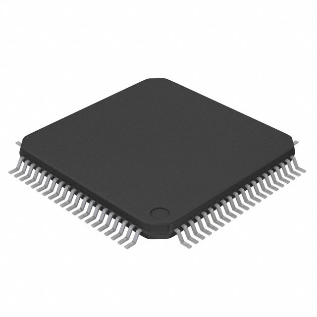
The STM32F378VCT6 integrates within a 100-pin LQFP (Low-profile Quad Flat Package) form, a standard that aligns with complex embedded designs requiring expanded I/O accessibility and high analog fidelity. The physical footprint enables substantial signal routing density while maintaining thermal efficiency suitable for mid-tier power demands. This 100-pin LQFP format directly supports broad peripheral interfacing, facilitating multi-channel ADCs, timers, and communication lines without pin multiplexing compromises often encountered in smaller packages.
The STM32F3 microcontroller family demonstrates package diversity, encompassing LQFP48, LQFP64, LQFP100, UFBGA100, and WLCSP66. Each format targets distinct design priorities: LQFP48 and LQFP64 ensure minimal board occupation for space-restricted modules, while LQFP100 and UFBGA100 provide elevated connectivity and signal integrity. UFBGA, with its array structure, further enhances electrical performance in high-speed domains at the cost of advanced PCB assembly requirements. WLCSP66, optimized for mobile or wearable application constraints, trades off pinout for a footprint nearing bare silicon.
Pinout optimization entails mapping microcontroller resources to achieve both minimal crosstalk and efficient signal flow. Alternate function remapping, a hallmark of STM32 series flexibility, requires forethought on hardware abstraction and future-proofing in case design revisions necessitate peripheral changes. Signal integrity, especially on analog-capable pins, is upheld through precise trace impedance calculation and via minimization. These tasks become paramount when assigning critical signals, such as high-resolution clocks or sensitive analog lines, which are directly susceptible to PCB layout artifacts. Early schematic capture and net assignment, aided by peripheral signal tables from reference manuals, streamline this process.
Effective decoupling is foundational to stable MCU performance. Layered decoupling capacitor networks—utilizing diverse capacitance values placed in close proximity to the VDD and VSSA pins—attenuate both broadband and high-frequency noise. Empirical practice suggests combining low ESR ceramic capacitors (0.1 µF) nearest the pins with larger bulk capacitances (4.7 µF–10 µF) positioned per power rail. Advanced layouts employ via stitching and ground plane segmentation to further protect analog domains from digital switching artifacts.
Load capacitance tuning is often required on oscillator input and output pins to achieve precise crystal startup and frequency stability. These values are determined by crystal datasheet specifications but may necessitate board-specific adjustments during prototyping, with consideration given to stray PCB capacitance and solder mask variations. Marker orientation on package top-face silkscreen aids automated optical inspection and placement accuracy, ensuring manufacturing traceability from pick-and-place through in-circuit testing and deployment.
Elevated design robustness arises when package selection synchronizes cost structure, component availability, and long-term maintainability. Projects leveraging the STM32F378VCT6’s LQFP100 unlock extensive application potential in motor control, sensor aggregation, and industrial automation, where persistent pinout clarity and analog precision are critical. The intersection of flexible pin mapping and stringent PCB attention yields scalable architectures, accommodating both current goals and unanticipated future expansions within the same hardware platform.
Electrical and thermal characteristics of STM32F378VCT6
Electrical and thermal behavior of the STM32F378VCT6 is defined by a detailed matrix of operational parameters essential for high-reliability embedded solutions. Voltage domains—VDD (core supply), VDDA (analog), VDDSD12 (digital), and VDDSD3 (peripherals)—exhibit stringent interdependencies; precision during power-up sequencing is paramount. Neglecting sequence order can trigger transient conditions or latch-up phenomena, often leading to latent failures. International EMC standards underscore the necessity of adhering to these supply constraints in densely interlinked circuit topologies.
Quantitative characterization spans static and dynamic I/O consumption profiles, with supply current values tied directly to system clock source, bus activity, and I/O toggle rates. It is critical to map workload scenarios during early modeling, capturing peak and quiescent currents tied to both peripheral enablement and firmware-directed sleep modes. Voltage range observance, especially across logic-level thresholds, demands rigorous validation against datasheet minima and maxima—system integration tests routinely reveal marginal violations due to board-level parasitics or cross-domain harmonics. Logic levels are notably sensitive when the MCU interfaces with disparate-voltage subsystems such as FPGAs or signal conditioners; clamp diodes and passive level shifters mitigate such coupling risks.
Thermal constraints emerge from junction-to-ambient thermal resistance (θJA), dynamically influenced by PCB layout, airflow, and enclosure design. Controlled impedance traces and thermal vias under the MCU package substantially cut thermal bottlenecks—bench measurements consistently demonstrate that multi-layer ground planes outclass single-layer counterparts in heat spreading efficiency. Calculating maximum permissible power dissipation involves not only idle and active core currents but also peripheral loads, especially when USB transceivers or precision timers operate under sustained high duty cycles. In environments surpassing standard ambient, forced-air cooling or heat sinks may become mandatory; without such measures, projected mean time to failure (MTTF) degrades sharply.
Layered evaluation, from electrical configuration through board-level thermal optimization, provides the foundation for high-performance deployment. Firmware designers benefit greatly from adaptive power management strategies, such as dynamic clock scaling and peripheral gating, to minimize worst-case current spikes. On the hardware side, investing in detailed thermal simulations, guided by empirical resistance models, streamlines enclosure selection and fosters iterative improvement in mass production runs. Ultimately, system longevity hinges on harmonizing these physical constraints with real-time operational demands—only then can maximum MCU utilization be realized within safe operational envelopes.
Environmental compliance and reliability features in STM32F378VCT6
Environmental compliance and reliability occupy central importance in the STM32F378VCT6 microcontroller’s value proposition. The device adheres to stringent RoHS3 and REACH requirements, underscoring its commitment to reduced hazardous substance content and regulatory acceptability across international markets. The ECCN 3A991A2 classification further cements its utility for global applications, particularly in sectors where export control and traceability are mandatory compliance factors.
Core to operational robustness is its performance under electromagnetic compatibility (EMC) and electrical overstress conditions. The STM32F378VCT6 undergoes comprehensive testing for ESD (electrostatic discharge), EMI (electromagnetic interference), latch-up resistance, and I/O current injection tolerance in accordance with prevalent IEC/JEDEC standards. These protocols ensure that devices exhibit high resilience in electrically noisy environments, lowering the likelihood of unpredictable faults or permanent damage during deployment in real-world industrial and medical systems.
Achieving optimal system-level immunity, however, extends beyond silicon-level safeguards. Effective integration leverages multiple layers of defense: schematic strategies such as RC filtering on susceptible pins, rigorous PCB layout with enforced ground separation for digital and analog domains, and the use of TVS (transient voltage suppression) diodes at board interfaces. Experience consistently shows that separating high-frequency switching traces from sensitive analog or communication lines further reduces the risk of EMI-induced malfunctions. Explicit attention to power distribution—by implementing low-impedance power planes and local decoupling capacitors—substantially enhances system stability under transient loads or environmental disturbances.
Robust software countermeasures play a supporting but critical role. Watchdog timers, regular self-diagnosis routines, and input validation algorithms collectively raise the bar for fault tolerance and graceful recovery alongside hardware strategies. Field deployments confirm that systematic error logging and real-time monitoring, when paired with effective exception handling flows, lead to dramatically improved recovery rates after exposure to spurious events.
A deeper insight emerges at the intersection of hardware design and application context. While the STM32F378VCT6 delivers baseline immunity, the surrounding system architecture ultimately governs the realized reliability. Proactive and deliberate risk management—incorporating predictive modeling of interference sources and recurring board-level reviews—can bridge the subtle gap between passing standard compliance tests and ensuring mission-critical field robustness. A disciplined approach to design not only meets environmental and reliability mandates but unlocks operational confidence in demanding deployment scenarios, from factory automation to medical instrumentation.
Potential equivalent/replacement models for STM32F378VCT6
Selecting viable replacement candidates for the STM32F378VCT6 requires a multi-dimensional assessment beyond superficial datasheet comparison. Within the STM32F3 microcontroller family, attention gravitates toward devices like the STM32F373 and broader STM32F37x lines due to their architectural alignment. Key technical factors—core type, flash/RAM size, peripheral equivalence, and operational voltage—form the backbone of any risk-mitigated substitution.
Hardware-level compatibility centers around the LQFP100 package shared by these models. Pinout congruency and the mapping of high-use functions (ADC channels, I/O flexibility, timer instances) demand careful validation, using not only reference manuals but also schematic overlays to preempt signal misalignments. Minor differences in peripheral integration—such as the availability of advanced-control timers or additional DACs—may subtly shift firmware or layout implications. The voltage domain tolerance, often cited in machine safety and industrial contexts, must align precisely to avoid unforeseen board-level rework or downstream certification lapses.
Migration scenarios necessitate a disciplined review of device errata, package marking schemes, and supply lifecycle status. Device family variants, while theoretically compatible, can diverge in regulator architectures, temperature ratings, and even in the behavior of brown-out resets. These factors impact both immediate drop-in strategies and longer-term multi-sourcing policies.
Anecdotal experience in revision control processes points to the need for a robust regression testbench when shifting between STM32F37x subset options. Minor firmware tweaks may be required to account for subtle timing or initialization sequence changes, particularly in mixed-signal designs where analog performance shifts with silicon respins. Documentation inconsistencies between product lines can further complicate migration, underscoring the value of proactive communication with silicon vendors and contract manufacturers.
Strategically, true equivalency is a layered construct—combining electrical, physical, and procurement dimensions. Streamlining future migrations benefits from early pinout discipline, conservative use of specialized peripherals, and assembly documentation that isolates MCU-dependent details. Industry observations show that investing in abstraction layers within firmware and hardware pays dividends when swapping MCUs mid-lifecycle or integrating alternate sourcing within a single bill of materials. These approaches reduce churn, enhance design resilience, and position the engineering organization to adapt rapidly to market-driven component shifts.
Conclusion
The STM32F378VCT6 microcontroller exemplifies a purposeful fusion of high-fidelity analog and digital subsystems within the STM32F3 family. At the foundation, its 32-bit ARM Cortex-M4 CPU integrates DSP instructions, substantially increasing computational throughput for real-time signal analysis, filtering, and control. The analog front-end incorporates multi-channel, high-resolution ADCs, DACs, and programmable analog comparators, delivering precise acquisition and conversion essential for instrumentation, metrology, and sensor fusion. Advanced calibration algorithms and adaptive sampling rates enable reliable data integrity even in demanding electromagnetic environments.
Digital connectivity is reinforced through native support for industry protocols including USART, I2C, SPI, and CAN, facilitating seamless integration with external sensors, actuators, and communication modules. Flexible I/O multiplexing, combined with scalable pin-count options, allows for rapid system partitioning and customized layouts. For power optimization, the device implements multi-domain voltage management, with distinct Vdda and Vddio rails to permit isolation of sensitive analog circuitry and controlled digital sections. Deep-sleep and dynamic clock gating strategies contribute to minimal standby currents, making the STM32F378VCT6 well-suited for portable and battery-operated platforms.
Package diversity presents tangible benefits. Choices spanning LQFP and BGA ensure compatibility across PCB assembly lines, supporting reflow profile adjustments and enhancing board-level reliability. This versatility affects not only initial prototyping but also end-product maintainability and field service strategies.
In practical deployment, leveraging the device’s reference designs accelerates performance validation and regulatory compliance. Close examination of errata and silicon revisions is prudent, as subtle design changes in analog blocks or peripheral mappings may impact time-critical control loops or measurement accuracy. The extensive documentation ecosystem, including application notes and low-level drivers, supports nuanced configuration, from ADC trigger synchronization to low-jitter PWM generation.
Forward-thinking engineering workflows anticipate supply chain volatility and lifecycle management by cross-referencing STM32F378VCT6 variants and associated longevity guarantees. Build-of-materials flexibility is preserved by designing for pin compatibility and firmware portability across the STM32F3 family, reducing risk in future scalability or platform migration.
The STM32F378VCT6’s architecture demonstrates an optimal balance of precision, integration, and adaptability. Continuous evaluation of peripheral interdependencies and power consumption trade-offs enables robust, cost-effective solutions for precision control, industrial automation, and connected measurement nodes. This device underscores the value of harmonizing analog accuracy with digital efficiency, a perspective vital when specifying microcontrollers for mission-critical, time-sensitive contexts.