


 >
>


Product overview: LDFMPVR STMicroelectronics linear voltage regulator
The LDFMPVR from STMicroelectronics operates as a high-performance linear voltage regulator, designed around the core priorities of stability, precision, and integration flexibility. Leveraging advanced process technology, the device achieves a finely tuned balance between low dropout voltage and robust load regulation. This manifests in reliable operation across a spectrum of input voltages, supporting both fixed and adjustable outputs. Internally, a sophisticated error amplifier architecture governs output stability while suppressing line and load transients—critical for circuits vulnerable to noise, such as analog front-ends or RF blocks.
The regulator's 500 mA output capability within a minimal 6-DFN footprint (2x2 mm or 3x3 mm) streamlines the layout process for densely populated PCBs, where thermal performance is frequently a bottleneck. This thermally optimized package, coupled with low quiescent current, mitigates self-heating and enhances system longevity, especially in battery-operated devices. Effective thermal resistance management is evident through the device’s copper pad configuration, which facilitates efficient heat dissipation even under continuous loading. Application in industrial and medical environments benefits from the regulator’s adherence to stringent noise and ripple specifications, minimizing electromagnetic interference and preserving signal integrity for sensitive sensors.
In practice, the LDFMPVR simplifies supply sequencing and facilitates the direct powering of core or analog domains through its adjustable output setting. A consistent upstream implementation involves deploying the regulator at strategic locations to isolate digital and mixed-signal subcircuits, enhancing cross-domain performance. Accumulated experience points to the regulator’s predictable characteristics in startup and load-step responses, which becomes invaluable for minimizing glitches in tightly timed operations or when transitioning between power modes.
A nuanced perspective emerges when considering long-term reliability. The device exhibits resistance to latch-up and maintains output regulation under fluctuating ambient conditions, aligning with extended maintenance cycles required by industrial machinery and portable instruments. It proves effective in scenarios demanding both rapid prototyping and final production, underscoring its role as a core building block in scalable power management frameworks.
This approach to voltage regulation—prioritizing precision, thermal resilience, and compactness—fits with emerging trends toward miniaturized, multi-domain architectures. Insights derived from iterative deployment highlight the importance of selecting regulator topologies that not only meet specification but also accommodate evolving system requirements, ensuring that design flexibility is embedded for future enhancements and unforeseen constraints. The LDFMPVR thus stands as a reference option where methodical engineering translates directly to system reliability and extended field performance.
Core features and benefits of LDFMPVR STMicroelectronics
The LDFMPVR linear regulator from STMicroelectronics integrates robust features designed for versatility and precision in modern power management. Operating effectively across an input range of 2.5 V to 16 V, the device adapts seamlessly to various supply architectures, including battery-powered systems and distributed rails found in complex embedded platforms. This flexibility is anchored by its ability to maintain regulation at a very low dropout voltage—300 mV maximum under a 500 mA load—thus enabling systems to fully exploit limited input headroom, reduce thermal stress, and bolster efficiency in both high- and low-voltage domains.
Engineers can extract significant value from the low typical quiescent current of 200 µA at full load, a specification that directly impacts battery longevity and thermal management in energy-constrained applications. In wearable electronics, sensor modules, and remote IoT nodes, lower self-consumption translates to prolonged operational lifespans and reduced cooling overhead, sharpening the design’s competitiveness.
The device offers both fixed and adjustable output options, serving a broad output voltage range from 0.8 V up to 12 V. Precision is paramount: fixed versions deliver a tight 1% output voltage accuracy, which safeguards noise-sensitive analog front-ends and tightly toleranced digital logic against supply drift. The adjustable variant, with its granular voltage setting capability, supports prototyping flexibility and last-mile optimization when adapting for specific load requirements or cascading multistage supplies.
Integrated logic-level shutoff controls enable straightforward power sequencing and system state management. The inclusion of a Power Good indicator further enhances design reliability, allowing downstream circuits to respond assuredly to valid power conditions and facilitating intelligent error handling on power-up or fault events. These features streamline firmware logic and board-level diagnostics, enhancing both safety and startup confidence.
Safeguards against fault conditions are engineered into the device’s core. Internal current limiting and thermal shutdown fortify its resilience, helping maintain stable operation from -40 °C up to +125 °C ambient. Experience shows that regulators with such safeguards markedly reduce board-level issues during design verification and field deployment. In environments subject to substantial temperature cycling or unpredictable operating loads, these protections minimize unplanned maintenance and help ensure robust, repeatable performance.
A nuanced understanding of these capabilities suggests that LDFMPVR is especially well suited for precision analog systems, multi-rail microcontrollers, and compact industrial nodes, where every millivolt and microamp matters. Its combination of low dropout, efficient housekeeping current, and system-focused features enables engineers to push design boundaries, striking a favorable balance between high performance and reliability—even under stringent constraints or evolving use cases.
Electrical characteristics and performance metrics of LDFMPVR STMicroelectronics
Electrical behavior and performance analysis of the LDFMPVR LDO from STMicroelectronics reveals critical factors for board-level voltage regulation. Built on advanced process technology, the LDFMPVR maintains precise output regulation across a wide spectrum of supply fluctuations and load steps. The core mechanism involves a low-dropout architecture with carefully engineered error amplification, enabling minimal deviation in output voltage during rapid current changes. Load regulation remains typically within the tens of millivolts, even as output current increases, an important trait for power integrity in dense digital logic and sensitive mixed-signal domains.
Line regulation is equally optimized, allowing the device to absorb variations in input voltage while delivering nearly constant output—established through a high-gain feedback loop that immediately corrects for external perturbations. The regulator's compensation profile is tailored for fast loop response, producing sub-millisecond recovery times after abrupt transients. This translates directly into stable rail voltages supporting clocked devices and analog signal chains, minimizing spurious resets or data corruption due to supply dips.
Design factors such as external capacitance (1 µF input, 2.2 µF output) have been experimentally validated to balance phase margin and transient robustness. Thermal behavior is well-contained; the LDFMPVR sustains operation down to -40 °C and up to +125 °C, using sophisticated temperature sensing and adaptive circuitry that throttles output or initiates shutdown under hazardous conditions. Short-circuit protection is not simply a reactive measure—it is tightly coupled to fault detection, rapidly latching and resetting in controlled cycles to avoid component overstress or PCB hot spots. Such proactive measures are highly effective when supplying edge devices or FPGAs subject to unpredictable load surges.
Applications run the gamut from memory modules demanding ultra-low ripple, to microprocessor cores with burst-mode current profiles. The LDFMPVR’s dynamic response ensures voltage droop is contained, and recovery is flat, allowing designers to avoid costly guard banding or over-provisioning. Real-world integration often validates simulation results—boards assembled with the LDFMPVR maintain less than 2% output error during combinational switching events, improving both efficiency and EMI resilience.
A less obvious advantage emerges from the regulator’s internal topology: by limiting quiescent current and managing soft-start routines, it provides stable initial voltage ramps without inducing inrush current loads on the upstream supply. This feature becomes essential in multi-rail systems, where simultaneous sequencing is required for correct peripheral initialization. The regulator’s design philosophy—prioritizing precise control, rapid fault recovery, and minimal parasitic effects—offers competitive utility, especially for engineers facing space, cost, and performance constraints in current-generation embedded systems.
Pin configuration and application circuitry for LDFMPVR STMicroelectronics
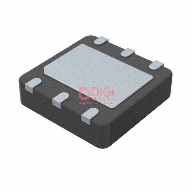
The LDFMPVR from STMicroelectronics features a compact DFN6 package, offered in both 2x2 mm and 3x3 mm footprints. This package choice substantially optimizes PCB real estate, allowing dense component placement and supporting advanced miniaturization strategies. With reduced loop area and minimized lead inductance, the DFN6 configuration significantly curtails parasitic capacitance and inductance—an essential factor in maintaining high-frequency stability and suppressing EMI in tightly packed layouts.
Pin assignments are deliberately straightforward: distinct terminals for VIN, VOUT, GND, EN (enable), and Power Good provide intuitive routing. Such clarity in pinout supports rapid schematic capture, especially when leveraging ECAD design tools with integrated component libraries. Traces can be kept short and direct, which is especially crucial in noise-sensitive analog or mixed-signal domains. In multilayer boards, adjacent ground pours beneath the package further attenuate conducted and radiated noise; designers have noted that this method often yields measurable improvements in transient response and output ripple reduction compared to less compact linear regulator layouts.
For adjustable output rails, the LDFMPVR implements external resistor networks on the FB (feedback) pin, adhering to standard voltage divider conventions. This architecture empowers engineers with granular control over output setpoints, accommodating custom system requirements without re-spinning the bill of materials or sacrificing efficiency at low currents. Integrating this flexibility into power architectures enables developers to consolidate supply variants, streamlining both prototyping and volume manufacturing. Strategic placement of these resistor elements—ideally as close as practicable to the FB and GND pins—mitigates PCB noise pick-up and minimizes error in voltage regulation.
Application circuits, as detailed in the manufacturer documentation, translate directly to both breadboard validation and mass production. The underlying topology is robust against layout variations, provided best practices—such as low-impedance ground routing and careful decoupling—are observed. In a variety of scenarios, from precision sensor supplies to auxiliary logic rails in embedded designs, the LDFMPVR demonstrates strong resilience to line/load perturbations and exhibits consistent start-up behavior. In-field observations have substantiated the value of integrating the Power Good output into system-level power sequencing logic, safeguarding downstream devices from undefined supply conditions.
When evaluating regulator choice, attention to the benefits of a purpose-designed pinout and airflow-facilitating package becomes increasingly evident. The LDFMPVR’s overall integration exemplifies effective trade-offs between compactness, performance, and ease of adoption—elements that, when synthesized skillfully, accelerate project timelines while minimizing system-level risk.
Application guidance for LDFMPVR STMicroelectronics: Capacitor selection and enable functions
Application engineering for LDFMPVR voltage regulators from STMicroelectronics centers on precise external capacitor selection and correct implementation of digital control features to achieve robust stability and predictable system behavior. The nuanced interaction between capacitance value, dielectric type, and ESR directly dictates the regulator’s dynamic response, noise performance, and reliability across diverse operating conditions.
For input decoupling, a minimum of 1 µF is specified, yet practical results show improved transient immunity when using capacitance values moderately above this threshold. Selection of multilayer ceramic capacitors significantly enhances performance due to their inherently low ESR and minimal impedance at high frequencies. However, the critical parameter is not simply ESR at ambient; real-world scenarios demand a holistic evaluation—ESR must remain within specified bounds from startup in cold conditions through thermal cycling and long-term component aging. Empirically, using capacitors rated with X7R or C0G dielectrics secures stability across common application environments and mitigates capacitance drift, especially in compact layouts subjected to board flex.
Output capacitance, at a recommended minimum of 2.2 µF, further fortifies load regulation and noise suppression. In advanced designs, paralleling multiple ceramic capacitors with slightly staggered values can flatten impedance peaks, extending the stability margin even under rapid load stepping or system-level EMI disturbances. Engineering judgement suggests verifying the composite capacitance as well as cumulative ESR to guarantee the regulator operates within its phase margin envelope over the life of the product. Simulating worst-case ESR scenarios, factoring in temperature rise, is essential in high-reliability or mission-critical circuits where self-heating or adjacent component influence can compromise regulator stability.
Enable functions, crucial for power management strategies, require meticulous signal integrity. The Enable pin must be tied via a well-defined logic-level driver or a fail-safe pull-down to guarantee deterministic on/off control. Margins must be observed for the voltage thresholds amidst power supply drift or noisy environments, preventing ambiguous states which could trigger erratic regulator behavior. Board-level experience highlights the risk: floating Enable pins have led to inadvertent latch-up or excessive quiescent current, underscoring the importance of predictable logic transitions mapped to system sleep/active cycles.
Power Good signaling, realized through open-drain architecture, expands facility for advanced supply sequencing and fault detection. Optimal performance is achieved by selecting a pull-up resistor value—typically within 10 kΩ to 100 kΩ—that matches the system’s logic interface requirements while minimizing propagation delay on the status indication. Integrating PG status into supervisory firmware allows real-time coordination with downstream loads, promoting safe startup sequencing and persistent rail monitoring. Notably, in multilayer PCB designs, routing the PG signal away from noisy switching elements preserves integrity and avoids false fault flags.
Fundamentally, a design approach that treats capacitor choice and digital control pins as interdependent system elements—rather than isolated components—yields more predictable, resilient regulator deployment. The nuanced combination of high-grade ceramic capacitors, rigorous ESR assessment, and disciplined digital pin handling forms the backbone of modern embedded power solutions, ensuring each LDFMPVR instance delivers consistent low dropout regulation with robust fault management. Optimal results arise from iterative design validation cycles that stress all relevant parametric limits, anchoring long-term reliability.
Package options and PCB recommendations for LDFMPVR STMicroelectronics
For the LDFMPVR voltage regulator family, STMicroelectronics offers two primary package formats: DFN6 in a 2x2 mm and DFN6 in a 3x3 mm footprint. Both are tailored to minimize board space, meeting the high-density requirements typical of portable systems, compact embedded devices, and miniaturized sensor nodes. The package choice directly influences thermal management strategies and component placement flexibility—critical factors during the initial layout phase for systems where PCB real estate is at a premium.
These packages comply with ECOPACK environmental standards, an important consideration for OEMs focusing on sustainable design and global regulatory mandates. The lead-free, RoHS-compatible construction not only streamlines qualification processes but also accommodates future product lifecycle needs without necessitating redesigns.
For successful integration, strict adherence to the PCB footprint and pad outline recommendations indicated by STMicroelectronics is essential. These specifications are engineered to maximize thermal conductivity from the regulator junction to the board, usually involving optimized copper area and via placement beneath the exposed pad. Experience shows that deviations from these guidelines—for instance, shrinking thermal pad dimensions to conserve space—can result in substantial increases in junction temperature and may trigger intermittent thermal shutdown events under load. To address this, leveraging multi-layer boards with direct via stitching beneath the DFN package is often deployed to enhance vertical heat spreading and ensure predictable temperature profiles even at elevated ambient conditions.
Electrical performance is also tied closely to the recommended footprint design. The provided layout minimizes parasitic inductance and resistance, which otherwise could impact transient response and output noise characteristics. In fast-switching applications or when powering sensitive analog circuitry, maintaining the manufacturer's pad design helps avoid performance degradation caused by unexpected EMI coupling or voltage ripple.
The interaction between package selection, thermal policy, and PCB layout not only frames the electrical and mechanical robustness but also modulates time-to-market. Integrating reference designs and simulation benchmarks early in the prototyping process using the official STMicroelectronics documentation often shortens design cycles and reduces re-spins. In practical deployment, coupling these practices with high-quality soldering, precise stencil design, and controlled reflow parameters leads to repeatable assembly yields and minimizes latent defects, underscoring the centrality of package-to-board synergy.
Balancing footprint precision, thermal architecture, and regulatory adherence is a persistent theme in low-dropout regulator designs. By emphasizing these interconnected domains, the risks of thermal bottleneck, EMI disturbance, or manufacturability setbacks are substantially reduced, facilitating scalable deployment from development platforms to volume production platforms.
Potential equivalent/replacement models for LDFMPVR STMicroelectronics
In addressing the selection of equivalent or replacement models for the LDFMPVR from STMicroelectronics, systematic attention to the device’s underpinnings and operational characteristics is pivotal. The LDFMPVR belongs to the LDFM series, characterized by precision regulation, low dropout performance, and a compact package, optimized for stringent voltage management in embedded systems. Core to the evaluation process is mapping the input voltage tolerance, output current provision, and, critically, the dropout voltage under worst-case load and temperature conditions. This directly affects both efficiency and thermal stability, particularly in densely populated designs with limited heat sinking.
Effective substitution hinges on a thorough cross-comparison of Linear Voltage Regulator ICs, especially those maintaining consistent performance across the LDFM family or reputable cross-vendors like Texas Instruments’ TPS7xx or ON Semiconductor’s NCP series. Regulatory logic features—including enable lines and Power Good (PG) outputs—require scrutiny, as discrepancies in logic levels, signal timing, or output structure can cascade into broader system-level compatibility issues, especially within power sequencing and diagnostic routines. Portfolio variants may present nuanced differences: for example, soft-start behavior, quiescent current, or package-specific thermal resistance, all meaningful in applications where inrush control or battery longevity carries significance.
Diligence in analyzing absolute maximum ratings versus recommended operating ranges can preclude silent reliability risks arising from marginal overspecification. Real-world board-level testing has shown that even minor deviations in PSRR (Power Supply Rejection Ratio) or transient response can manifest as functional glitches, particularly in analog front-ends or precision ADC/DAC environments. Incorporating derating strategies and simulating stressed conditions under variant regulator candidates validates robustness prior to production design freeze.
A practical framework often involves shortlisting viable alternatives using parametric search engines, followed by bench verification. Emphasis on accurate assessment of PCB thermal performance with candidate regulators is vital; simulation tools can assist, but measured results-of-junction temperature under full-load offer actionable data for iterative refinement.
Ultimately, optimal regulator substitution is not simply a datasheet-driven exercise. It draws upon layered diligence: device physics, system context, empirical validation, and a bias toward conservative design margins. Factoring in supply chain continuity, package availability, and future scalability options further elevates long-term project resilience, ensuring the replacement strategy aligns not just with electrical requirements, but also the operational realities of modern electronics production.
Conclusion
Integrating the LDFMPVR linear regulator from STMicroelectronics into precision electronic design demands understanding its core architecture and function. Central to this device is the low dropout topology, which minimizes voltage differential between input and output, enhancing power efficiency in scenarios where supply headroom is limited. A low dropout characteristic is not just advantageous for energy-sensitive portable designs; it also helps mitigate thermal buildup in dense PCB layouts, directly impacting system reliability. The device’s circuit incorporates advanced bandgap references and tight error amplifier feedback, underpinning its high output voltage accuracy. This precision is vital for noise-sensitive signal chains and analog circuitry, where even minor supply variations can compromise data acquisition fidelity.
Robust voltage regulation emerges not only from intrinsic silicon performance but also from careful interface and integration. The LDFMPVR offers logic-compatible enable and Power Good (PG) signals, enabling streamlined system sequencing and diagnostic feedback. For design teams orchestrating complex startup routines or fault monitoring, the easy interfacing of these digital controls with microcontrollers or sequencers can expedite verification and boost operational safety margins. Rigorously specifying input and output capacitors—both in value and ESR tolerance—directly influences regulator stability and transient response. In practice, using low-ESR ceramic capacitors close to the device terminals suppresses voltage dips during rapid load changes and fortifies electromagnetic compatibility, especially critical within multilayer boards or RF-adjacent platforms.
Mechanically, STMicroelectronics’ provision of rugged, thermally optimized packaging for the LDFMPVR suits applications characterized by restricted board space and high component density. For instance, in precision instrumentation or compact sensor modules, minimizing regulator footprint and maximizing heat dissipation area permit higher packing ratios while retaining thermal limits. During layout, short, wide traces between input, output, and ground pins grant lower impedance paths, which, in prototyping, directly translates to improved voltage regulation during dynamic conditions. Thoughtful component placement also curtails current loop area, reducing noise injection into adjacent analog stages.
An often-underestimated aspect of integrating such regulators lies in lifecycle management and supply assurance. With STMicroelectronics’ reputation for long-term device support, procurement teams can align BOM strategies around anticipated production runs, shielding projects from costly redesigns linked to obsolescence. This foresight, paired with parametric evaluation—checking dropout, PSRR, and quiescent current under realistic workloads—results in robust, durable system architectures.
In summary, the LDFMPVR forms a nexus between analog fidelity, digital controllability, and mechanical resilience. Its layered strengths—rooted in fundamental circuit design and amplified by practical engineering decisions—render it a critical building block for precision-driven, space-constrained electronics. Judicious integration yields not only technical compliance but also design margin, positioning development teams for scalable innovation in demanding operating environments.


