


 >
>


Product overview: L6393D half-bridge gate driver by STMicroelectronics
The L6393D by STMicroelectronics serves as a high-voltage half-bridge gate driver, engineered specifically for demanding power conversion applications leveraging N-channel power MOSFETs or IGBTs. Central to its performance is the integration of high-side and low-side drivers capable of managing rail voltages up to 600 V, enabled by ST’s proprietary BCD™ “offline” process. This technology merges Bipolar, CMOS, and DMOS transistors on a single die, providing tight control over power, logic, and level-shifting functionalities within a compact SO-14 footprint. Such integration addresses the space and board complexity constraints frequently encountered in modern industrial designs.
Examining its electrical interface, the L6393D supports CMOS and TTL logic inputs down to 3.3 V, facilitating direct connection with microcontrollers or digital signal processors operating at reduced voltages. This compatibility streamlines control circuitry, reducing the need for interface buffers or level-shifting stages that risk adding latency and system bottlenecks. The robust level-shifter embedded in the chip ensures reliable signal integrity across a wide operational voltage window and minimizes propagation delays—a critical consideration for high-frequency switching applications such as electronic drives and advanced motor control algorithms.
The device architecture incorporates dedicated logic for shoot-through prevention and cross-conduction immunity. By integrating dead-time control, it guarantees that both the high-side and low-side power switches are never simultaneously on, thus preventing catastrophic short-circuit failures in bridge topologies. Protective features extend to under-voltage lockout mechanisms for both driver outputs, further safeguarding system reliability against transient brownouts or start-up events. Such hardware-level enforcement of safety protocols optimizes reliability, particularly in industrial automation and motor drive platforms where uptime and fault tolerance are paramount.
From an application standpoint, the L6393D’s high-voltage tolerance allows seamless deployment in AC-DC and DC-DC converters, as well as lighting ballasts and general-purpose inverters. The half-bridge topology, when implemented with L6393D, efficiently manages bidirectional power flow and precise pulse width modulation (PWM) control. In practical deployment, leveraging the compact SO-14 package simplifies PCB layout, notably reducing parasitic inductances in the gate driver loop, which is essential for minimizing electromagnetic interference and obtaining faster switching edge rates. Design experience shows that pairing L6393D with fast-recovery power devices can substantially enhance system efficiency, provided trace lengths between driver and power switches are kept short and high-speed signal integrity is duly maintained.
The high-voltage bootstrap supply integrated in the L6393D eliminates the need for external bootstrap diodes or resistors, improving reliability and simplifying bill of materials (BOM) management in high-density designs. Furthermore, its tolerance for negative transients and robust ESD protection support deployment in factory environments subject to frequent electrical disturbances.
A nuanced insight is that the interplay between the driver’s source/sink capability and the choice of power switch directly impacts overall converter efficiency, particularly at high switching frequencies. Accordingly, optimizing gate impedance network parameters in conjunction with the L6393D’s drive strength allows for tailored dV/dt control, suppressing ringing and improving EMI performance without sacrificing switching speed. This flexibility makes the L6393D a strong candidate for both new designs and retrofit upgrades in legacy equipment, where efficiency improvements and footprint reduction are continuous engineering objectives.
Overall, the L6393D’s architecture and feature set offer a robust, flexible foundation for next-generation power conversion systems seeking reliable operation in harsh industrial contexts, with design choices enabling both ease of integration and enhancement of system robustness.
Functional architecture of the L6393D half-bridge gate driver
At the heart of the L6393D lies a thoroughly integrated half-bridge gate driver topology purpose-built for robust power conversion systems. The architecture centers on a high-voltage floating section, which reliably supports voltage differentials up to 600 V. This configuration enables seamless driving of both high-side and low-side N-channel MOSFETs or IGBTs without the need for bulky external level-shifting or isolated supplies. By leveraging the floating section, the L6393D can maintain control logic referenced to the source of the high-side device, ensuring proper turn-on performance across a wide common-mode voltage swing, a critical factor for bridge-based power topologies.
Examining the output structure, the device integrates two principal gate driver channels: HVG for high-side and LVG for low-side switching, each precision-engineered to deliver symmetrical, low-impedance paths for rapid switch transitions. Fast rise and fall times are achieved through dedicated output stages with strong sink and source currents, minimizing shoot-through and power losses during high-frequency operation. The internal bootstrap diode is seamlessly co-packaged, streamlining the high-side gate bias generation and reducing component count—a clear advantage in compact, space-constrained designs.
A configurable deadtime control mechanism is embedded, granting designers granular control over shoot-through immunity during switching events. This feature is essential in motor drives, power inverters, and DC-DC converters, where fine-tuning deadtime directly impacts efficiency and device longevity. In practical implementation, careful adjustment of deadtime enables the optimal balance between cross-conduction prevention and switching losses, especially in high-switching-frequency applications where timing margins are minimal.
The L6393D’s interfacing logic offers compatibility with 3.3 V and 5 V control signals, ensuring straightforward integration with diverse microcontrollers and DSPs. Additionally, the internal charge pump circuitry supplements bootstrap operation, maintaining robust gate drive even during low-duty-cycle conditions—a key enabler in scenarios with variable or asymmetrical switching patterns.
A distinguishing aspect is the uncommitted comparator, accessible for custom protection schemes. Designers can realize fast-acting overcurrent, overtemperature, or fault detection loops without resorting to external comparators. Experience has shown that integrating system-level protection internally not only improves response times but also simplifies board layout and reduces susceptibility to noise. Subtle nuances in comparator threshold setting and filtering can provide an application-specific trade-off between immunity to transients and responsiveness.
Upon close analysis, the L6393D encapsulates the trade-space required by modern power stage engineering: high integration, robust protection schemes, dynamic adaptability, and operational resilience. Superior device coordination is achieved by orchestrating internal features such as deadtime control, charge pumping, and bootstrap management, all within a thermally-optimized footprint. This core engineering synergy presents a versatile platform suitable for industrial motor control, uninterruptible power supplies, and renewable energy systems, where reliability and efficiency drive design priorities.
Key features and performance specifications of the L6393D half-bridge gate driver
The L6393D half-bridge gate driver is engineered for high-voltage, high-performance power switching applications. Central to its architecture is a 600 V rail capability, enabling direct interfacing with industrial power stages while supporting standard bus voltages in motor drives and power conversion. This voltage headroom, reinforced by robust process technology, mitigates the risk of avalanche breakdown during fault events and transient overvoltages, favoring long-term device reliability.
Driving both high-side and low-side power switches, the L6393D delivers source currents up to 290 mA and sink currents up to 430 mA, ensuring robust turn-on and turn-off performance even with larger gate loads. Fast switching characteristics—75 ns rise and 35 ns fall times with a 1 nF gate load—enable efficient hard-switching topologies, where minimizing switching losses and electromagnetic interference is paramount. This rapid transition profile directly addresses thermal challenges seen in compact, high-density PCB layouts.
The logic interface accommodates CMOS/TTL levels down to 3.3 V, facilitating seamless integration with contemporary control platforms including advanced microcontrollers and digital signal processors. This feature streamlines system development, eliminating the need for level shifters and reducing propagation error, particularly in synchronized multi-channel environments.
Deadtime adjustment, realized through an external resistor, empowers precise control over commutation intervals between high-side and low-side transitions. Fine-tuning deadtime is crucial in avoiding cross-conduction phenomena, thus enhancing efficiency and system reliability. In iterative hardware development, such flexibility shortens design cycles and supports adaptation to diverse switching devices with varying recovery characteristics.
Integration of the bootstrap diode within the IC not only simplifies the bill of materials and layout but also reduces overall parasitic capacitance and inductive pathways. This containment leads to a lower susceptibility to voltage overshoot and ringing, observable during high-frequency edge transitions, and increases gate-driving robustness in aggressive switching scenarios. By consolidating the bootstrap function on-chip, recurring issues with diode selection and external placement are sidestepped, producing repeatable and stable gate voltage behavior.
The on-chip, uncommitted comparator opens avenues for implementing custom protection schemes, such as current limiting or overtemperature shutdowns. In field deployments demanding strict fault tolerance, leveraging this comparator facilitates targeted protection with minimal propagation delay, often outperforming discrete solutions in precision and board area efficiency.
High dV/dt immunity (±50 V/ns) across full temperature range exemplifies the driver’s resilience in noisy environments. This immunity preserves gate integrity during rapid line and load transients, common in inverter output stages or switched-mode power supplies, eliminating nuisance triggering or spurious gate events. Designers targeting high-reliability, high-uptime installations gain a substantive edge from this specification.
Low steady-state current consumption is achieved by design and directly elevates the efficiency ceiling in applications sensitive to standby losses—such as battery-powered actuators or energy-critical industrial modules. Furthermore, the environmental compliance of the ECOPACK® ROHS-certified SO-14 package supports integration into global product lines without concern for regulatory barriers, streamlining procurement and lifecycle design.
In practice, deployment of the L6393D consistently reveals improved layout compactness, more predictable switching behavior, and enhanced observability of protection functions. Configuring the driver in multi-phase power topology demonstrates clear reductions in shoot-through events and gate ringing, empirically supporting the integration choices made at the architecture level. Distilling these characteristics illustrates the device’s suitability for scalable, modular power system designs, where the interplay of speed, protection, and reliability defines engineering success.
Input and control logic in the L6393D half-bridge gate driver
Input and control logic in the L6393D half-bridge gate driver is engineered for adaptable management of output states, crucial for optimizing performance in motor drive and power switching contexts. The interface employs two primary logic signals, PHASE and BRAKE, each entering the driver’s internal logic to dictate the behavior of the high-side (HVG) and low-side (LVG) outputs under various operating scenarios. The PHASE signal determines the conduction direction, facilitating bidirectional control and alternate conduction paths by toggling HVG and LVG accordingly. This underpins efficient motion control and enables seamless direction reversal in applications such as brushed DC motor drives, where precise phase steering enhances system responsiveness and torque accuracy.
The BRAKE input serves a dual function, significantly elevating control fidelity. When asserted high, it engages regular half-bridge operation in tandem with PHASE, yielding flexible switching sequences. Conversely, when BRAKE transitions low, the internal logic overrides PHASE, forcing the LVG output ON and HVG OFF, regardless of phase state. This decisively establishes a rapid slow decay mode, vital for closing current paths and quickly dissipating energy. In brush DC and stepper motor systems, this logic directly supports dynamic braking and controlled current recirculation, mitigating overvoltage conditions and curbing oscillatory behavior during active deceleration. Field experience indicates that leveraging this BRAKE-initiated decay facilitates smoother stop times and reduces stress on switching MOSFETs, especially in high-inertia loads.
Integral to safe and efficient switching is the implementation of externally controlled deadtime via the DT pin, which allows precise deadtime tuning beyond the constraints of fixed internal presets. Deadtime acts as a critical window between the turn-off of one output and the turn-on of its complement, effectively preventing shoot-through events—a condition where high- and low-side switches inadvertently conduct simultaneously, causing destructive high-current spikes. Adjustable deadtime is especially beneficial in circuits operating with wide-ranging MOSFET gate charge characteristics or under varying temperature and load conditions, where optimal timing margins can significantly reduce switching losses, electromagnetic interference, and thermal buildup.
Carefully matching deadtime to device and system specifics not only enhances efficiency but also extends reliability. In high-frequency applications—such as power inverters or synchronous rectifiers—minute calibration of the DT pin enables designers to balance minimal conduction overlap with maximum operation speed, translating to higher overall power conversion efficacy. Subtle but noteworthy, adjusting deadtime dynamically in response to load changes has demonstrated measurable improvements in system durability, minimizing the risk of cross-conduction even under transients.
Synthesizing control logic with fine-grained deadtime management, the L6393D architecture facilitates granular output steering for robust motion and power control, while offering mitigation mechanisms for failure-prone conditions common to high-speed switching environments. The interaction between PHASE and BRAKE and the adjustable deadtime algorithms thus delivers a versatile platform for both foundational motor control and advanced switching power stages, supporting both high safety margins and performance optimization.
Electrical and thermal operating parameters for the L6393D half-bridge gate driver
Effective deployment of the L6393D half-bridge gate driver requires precise alignment with its defined electrical and thermal specifications. The device is engineered to operate reliably within a high-voltage domain, supporting an absolute maximum rail of 600 V. This capability enables robust performance in motor control, power conversion, and industrial drives where voltage transients and noise immunity are recurrent challenges. The logic supply voltage is typified at 15 V, maintaining operational integrity down to 10 V, which offers a safety margin against supply sag in transient-heavy environments. Compatibility with both 3.3 V and 5 V logic interfaces enhances system versatility, streamlining integration alongside a range of controllers and microprocessors.
Input threshold levels are tightly controlled to ensure clean logic recognition, which is critical for noise-affected industrial settings. Reliable logic interfacing extends beyond compliance; it simplifies mixed-voltage system architectures and mitigates false triggering from parasitic coupling. Semiconductor processes used for the L6393D enforce stringent timing characteristics, with minimum rise and fall times specified at 75 ns and 35 ns respectively under standard test loads. Consistent switching performance at these edges is central to gating fast-switching MOSFETs or IGBTs, contributing to compact dead times and efficiency in synchronous power stages.
Output impedance and intrinsic R_DS(on) are optimized to minimize conduction losses while safeguarding against overcurrent scenarios across the full industrial temperature spectrum. This careful balancing act translates to tangible efficiency improvements, especially under elevated thermal loads. The on-chip comparator remains functional provided that both the VCC and high-side supplies exceed their respective undervoltage lockout thresholds, which forms an implicit layer of system protection. This ensures the gate driver responds predictably during brownouts or start-up sequences, safeguarding downstream power devices.
Thermal considerations rely heavily on real-world PCB design choices. While the L6393D exhibits low static dissipation—attributable to efficient CMOS and high-voltage processes—steady, high-frequency operation demands thoughtful thermal mitigation. Wide copper pours underneath the device and via arrays tied to ground are standard layout techniques, greatly reducing local temperature rise and preventing long-term parameter drift. For power stages where enhanced cooling is essential, heat-spreading laminates or modest external heat sinks further extend reliability. Even minimal airflow from nearby fans can meaningfully lower junction temperatures, maintaining robust timing parameters over the service life.
Operating temperature compliance spans both ambient and junction thresholds, matching industrial reliability expectations. In demanding prototypes, close attention to board-level heat spreading can reveal hidden thermal bottlenecks, especially in dense, multi-driver configurations. Pre-layout thermal simulation offers early insight, and measurement during in-situ validation—such as placing thermocouples at package leads or monitoring rear-side copper—proves invaluable for correlation.
The integration of careful electrical boundary management and proactive thermal practices distinguishes high-performing designs from merely functional ones. A nuanced understanding of these interdependencies enables circuit architects to achieve not just nominal operation, but sustained system robustness, even under variable grid conditions or in electromagnetically noisy environments. High-frequency, high-voltage applications particularly reward this approach, where subtle inefficiencies or thermal hotspots can erode long-term reliability.
Ultimately, the L6393D’s optimized design and adaptable integration parameters empower efficient, reliable high-side and low-side gate switching. Leveraging its intrinsic protections, judicious PCB layout, and system-level thermal insight yields a durable half-bridge solution, ready to meet the rigorous demands of modern industrial electronics.
Application scenarios for the L6393D half-bridge gate driver
Application scenarios for the L6393D half-bridge gate driver emerge foremost from its high-voltage withstanding capacity—capable of operating with supply rails up to 600 V—and from the flexibility embedded in its logic interface. The device’s half-bridge architecture supports both single- and three-phase motor configurations, making it highly suited for home appliances such as washing machines, HVAC compressors, and variable-speed fans. Rapid signal propagation and desaturation detection contribute to precise PWM control, directly impacting torque ripple mitigation and acoustic noise reduction in these systems.
At the industrial drive and robotics level, the L6393D’s input structure allows galvanic isolation schemes while maintaining deterministic switching. This becomes crucial in factory automation robotics, where consistent dead-time insertion and shoot-through protection guard against cross-conduction—a leading cause of MOSFET and IGBT failures under dynamic load conditions. Practical deployment in these environments often reveals the advantage of the L6393D’s operational robustness during power-line transients and its resilience to motor back-EMF, both of which are common in long-term use.
The L6393D integrates bootstrap diodes and dedicated undervoltage lockout protections, addressing efficiency and safety trade-offs found in switched-mode power supplies. In high-frequency full-bridge DC-DC conversion and inverter scenarios, this integration reduces the external component count, streamlines heat management, and minimizes parasitics that can introduce electromagnetic interference. Compact driver modules for automation benefit from the monolithic design, directly supporting dense PCB layouts and facilitating compliance with regulatory creepage and clearance requirements—even as supply voltages increase.
HID electronic ballast circuits and other capacitor-charging supplies require high-speed gate drive with reliable charge-pumping at hundreds of kilohertz. The L6393D’s fast turn-on/turn-off capability enables optimal lamp strike and stable operation during run-time waveform modulation. The integrated fault signaling allows seamless system-level fault management, preventing catastrophic failures in multiphase array circuits. By embedding start-up and protection features, the L6393D eliminates the need for external supervisory ICs, which in turn reduces procurement complexity and streamlines qualification processes.
Application strategies favoring miniaturization and system-level integration prioritize devices that unify logic compatibility, fast switching, and protection. Here, the L6393D stands out, as leveraging its built-in features yields reduced Bill of Materials cost, enables power section footprint shrinking, and simplifies PCB trace routing—particularly under constraints posed by multi-layer board stacking and automotive AEC-Q100 derived requirements. A layered approach to motor and power supply platform design benefits from such integration, balancing the need for scalability with operational safety.
An implicit insight from widespread field usage highlights the L6393D’s tolerance to layout imperfections and its capacity to maintain stable operation even in presence of moderate ground bounce or supply ripple. This real-world resilience makes it a strong candidate for rapid prototyping and iterative design where time-to-market and reliability are both paramount. The architectural philosophy underlying the L6393D, emphasizing protection, integration, and control fidelity, enables engineering solutions that are both robust and adaptable, reflecting evolving requirements in high-efficiency power electronic systems.
Bootstrap circuit design considerations with the L6393D half-bridge gate driver
Efficient bootstrap circuit design substantially influences the robustness and reliability of the L6393D half-bridge gate driver, especially regarding high-side MOSFET switching. The internal bootstrap mechanism in L6393D, distinct from conventional implementations, integrates a patented high-voltage DMOS device in series with a diode and synergizes with a synchronized charge pump. This configuration minimizes parasitic leakage paths, decreases external component reliance, and reinforces system integrity in noise-sensitive environments. It further reduces the complexity and board space by superseding fast external diodes.
The choice of the bootstrap capacitor (C_BOOT) governs charge availability and voltage stability. Because C_BOOT must routinely deliver adequate gate drive energy without significant droop, the established method leverages the ratio of MOSFET gate charge to drive voltage (Q_gate/V_gate) as the base value, but seasoned engineers adopt an order-of-magnitude margin to protect against undervoltage in extended on-state scenarios and charge losses from parasitic elements. For instance, with a 30 nC gate charge at 10 V yielding a minimum of 3 nF, a pragmatic C_BOOT selection of 100 nF hedges against voltage dips below 300 mV, even as tolerance, leakage, and layout imperfection stack against theoretical estimates. Overdesigning the bootstrap cap to support longer high-side conduction cycles proves advantageous in motor control and inverter applications where persistent HVG enhancement is critical.
Bootstrap path resistance, defined by the DMOS device’s R_DS(on), introduces nontrivial voltage drops during high-frequency switching regimes. Real-world implementation involves predicting cumulative losses due to repeated charging events—these become significant as switching rates rise and gate drive current demand escalates. Empirical bench measurements reveal that DMOS path drop can impair high-side MOSFET turn-on speed and completeness in edge-case operating points, potentially degrading system efficiency or reliability. In such contingencies, supplementing the bootstrap path with an external high-speed diode may restore sufficient charging, albeit at the cost of marginal leakage current and board complexity.
Adaptive attention to actual operating conditions yields optimal gate driver performance. Factoring prolonged high-side conduction, greater leakage due to temperature or layout, and erratic supply voltages into C_BOOT sizing and bootstrap path design ensures consistently high charge delivery. Practical experience demonstrates that meticulous bootstrap planning directly correlates with minimized switching losses and robust protection against shoot-through events—a testament to the importance of comprehensive consideration in power-stage engineering.
Strategically, leveraging L6393D’s integrated bootstrap solution offers pronounced advantages in compact, high-reliability drives. Recognizing the subtle interplay between gate charge, conduction intervals, path impedance, and external supplementation is essential. A rigorous approach—moving beyond datasheet recommendations to scenario-specific tuning—elevates the performance and longevity of high-side switching designs.
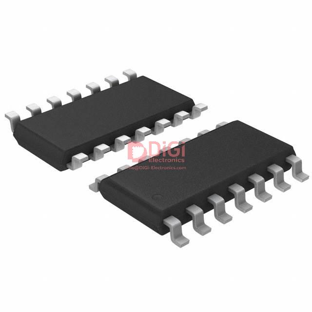
Mechanical and packaging information for the L6393D half-bridge gate driver
The L6393D half-bridge gate driver is presented in an industry-standard SO-14 ECOPACK® package, engineered for compliance with RoHS and contemporary environmental standards. This packaging format is optimized for high-density boards, utilizing a low-profile design to streamline integration into advanced power assemblies where spatial constraints demand compact component selection. The SO-14 package geometry ensures robust solder joint reliability during reflow assembly and provides precise pad alignment, which mitigates risks of tombstoning or misregistration even when automated placement systems encounter board-level warpage. Enhanced thermal dissipation is an intrinsic feature—ECOPACK® materials enable efficient heat flow from the die to the PCB, supporting stable gate driver operation under elevated module temperatures.
Pin accessibility is clearly prioritized, with standardized pin mapping and symmetrical lead distribution facilitating error-free routing and minimizing signal path inductance. Such characteristics reduce parasitic interactions that can compromise switch timing accuracy in high-frequency inverter topologies. Reliable electrical connectivity is maintained even in multi-layer board layouts with critical ground plane design, addressing common challenges with impedance control and cross-talk suppression. The package footprint supports rapid design cycles, especially when replicating driver channels across multi-phase platforms or updating legacy boards, due to alignment with typical auto-router and solder stencil parameters.
Designers benefit from comprehensive mechanical data and dimensional tolerances provided directly in ST’s documentation, empowering streamlined DFM analysis and straightforward configuration with existing CAD libraries. Real-world use demonstrates that this envelope accommodates inspection routines such as AOI and in-circuit probing, enhancing production yield and decreasing NPI risks. Notably, adopting the L6393D in densely packed environments consistently results in lower EMI emissions compared to bulkier alternatives, attributable to tight lead pitch and shielded package edges.
Selecting components like the L6393D in SO-14 format leverages an optimal intersection of manufacturability, thermal handling, and circuit reliability—key enablers for next-generation power electronics where gate driver efficiency and layout flexibility serve as pivotal determinants of system-level performance.
Potential equivalent/replacement models for the L6393D half-bridge gate driver
When considering substitution for the L6393D half-bridge gate driver in power conversion and motor control circuits, several technical layers demand analysis. At the core, the replacement device must sustain high-side and low-side switching across voltages up to 600 V or above. Robust high-voltage rail capability ensures reliability under demanding conditions, such as inverter legs or wide input ranges in power supplies. Integrated bootstrap diodes or circuitry streamline symmetrical gate drive for external MOSFETs and IGBTs, minimizing the need for discrete auxiliary components and supporting compact PCB layouts in surface-mount assembly.
Critical output drive strength and switching speed must be assessed, as these parameters directly influence propagation delay, turn-on/off loss, dV/dt immunity, and system efficiency. Gate drivers with similar sinking and sourcing currents to the L6393D deliver matching rise/fall times, avoiding mismatched transitions that can increase switching losses or degrade EMI performance. Devices like the L6390 and L6392 from the same vendor line maintain output dynamics close to the original, whereas alternatives from Texas Instruments, Infineon, or ON Semiconductor may offer enhanced transient response through optimized output buffers.
Advanced protection, including under-voltage lockout and programmable deadtime control, requires detailed verification. These features are pivotal for half-bridge configuration stability, blocking shoot-through and eliminating erratic gate drive under line sags or fault events. Deadtime trimming influences both efficiency and robustness—incorrect configuration can lead to catastrophic cross-conduction failures. Devices supporting adjustable deadtime, whether via external resistors or logic pins, simplify tuning during prototype validation and facilitate iterative design refinement.
Package compatibility, including pinout symmetry and thermal dissipation capacity, impacts production flow and rework effort. Surface-mount form factors, such as SO-16 or small-outline packages, support re-spin agility and maintain alignment with mature production lines. Subtle differences in pin assignments or thermal pads between candidate replacements can effect layout modifications or constrain heat extraction in dense assemblies. Experienced practitioners routinely cross-reference mechanical drawings and verify solderability, mitigating late-stage board spins.
Selection of a truly equivalent substitute always necessitates cross-checking absolute maximum ratings, logic input thresholds, and timing characteristics documented in vendor datasheets. Granular review of enable thresholds, input pulse width constraints, and latch-up immunity preserves seamless system operation post-replacement. Embedded insights highlight competitive second-source drivers with enhanced robustness at extreme edges—such as higher CMTI ratings or negative voltage survivability—potentially elevating long-term reliability beyond the original selection.
Application scenarios benefit from empirical evaluation: bench validation with gate drive oscilloscopes, thermal cycling under full current loads, and logic stress tests all illuminate subtle divergences in functional behavior. In practice, leveraging sample quantities for board-level drop-in trials reveals ergonomic nuances, facilitating confident migration between gate drivers without risking operational anomalies or costly production delays.
Conclusion
The L6393D half-bridge gate driver from STMicroelectronics demonstrates a tightly integrated architecture aimed at facilitating high-voltage half-bridge circuits in compact environments. At the core, the device incorporates both high-side and low-side gate driving capability, enabling efficient switching of external power MOSFETs or IGBTs across a broad operating voltage range. The inclusion of a built-in bootstrap diode, a distinctive feature for minimizing ancillary component count, significantly simplifies board layout and improves system reliability by reducing parasitic inductance and potential points of failure—a critical advantage in densely populated industrial control boards.
High-speed output stages ensure rapid response times and crisp switching transitions, directly impacting overall system efficiency by mitigating losses associated with gate charging and discharging delays. The propagation delay characteristics, combined with the optimized drive strength, enable precise timing control in motor drives and inverter systems, where synchronization between upper and lower switches is imperative for preventing shoot-through and achieving robust torque modulation. The driver’s compatibility with direct logic-level signals eliminates the need for level-shifting circuitry, further streamlining the design process and enabling direct interfacing with modern microcontrollers or DSPs used in advanced control algorithms.
Robust system-level protection mechanisms within the L6393D—such as under-voltage lockout and input filtering—offer significant insurance against operational faults and disruptive transients common in power systems and motor applications. These features not only enhance the resilience of the gate driver but also extend the service life of switching devices under demanding electrical conditions. Experience from fast-prototyping cycles reveals the practical value of fault detection integration: rapid fault isolation and recovery simplify both debugging and compliance with functional safety standards, accelerating validation phases and shortening time-to-market windows.
Deployment in industrial motor control scenarios showcases the utility of the L6393D’s compact footprint and functional density, allowing seamless implementation in constrained spaces like power tool controllers or HVAC actuator boards. The device’s versatility has also been noted in the context of modular inverter blocks, where consistent gate drive characteristics facilitate paralleling strategies and scalable designs. Selection of the L6393D as a platform component inherently reduces design risk, thanks to the predictable performance envelope and comprehensive documentation supporting parametric optimization for application-specific needs.
A nuanced appreciation of the device’s underlying circuit topology and interfacing conventions reveals critical leverage points: harnessing the integrated bootstrap diode for space and cost savings, exploiting the fast switching response for high-frequency operation, and aligning gate drive strengths with load characteristics to minimize EMI emissions in mixed-signal environments. The L6393D’s synthesis of functional integration and robust protection solidifies its status as a preferred solution for specifying high-voltage half-bridge applications where reliability, efficiency, and design agility are paramount.


