>
>


Product overview of the PL602-03SC-R by Microchip Technology
The PL602-03SC-R from Microchip Technology represents a precision-engineered clock buffer and oscillator module leveraging a low phase noise CMOS crystal oscillator core. This architecture prioritizes noise resilience and signal purity, supporting output frequencies from 48 MHz up to 100 MHz. At its foundation, the device utilizes a crystal input operating between 12 MHz and 25 MHz. Internal frequency multiplication circuits ensure efficient generation of high-frequency reference clocks while maintaining stability across a range of supply voltages and temperature profiles.
To achieve optimal phase noise and jitter performance, the design integrates advanced on-chip PLL (phase-locked loop) filtering and precision bias generation. This results in sub-picosecond RMS jitter, a critical factor in high-speed communication links and data converter clocks where signal integrity cannot be compromised. System-level engineers encounter tangible benefits in eye diagram clarity and bit error rate reduction, directly attributable to the PL602-03SC-R’s low additive noise characteristics. Unlike discrete oscillators paired with external buffers, this monolithic solution substantially simplifies PCB layout while minimizing clock distribution skew.
The buffer’s CMOS output driver is tailored for low output impedance and sufficient drive strength, supporting multiple parallel loads or longer trace lengths without significant degradation. This feature is directly applicable in clock trees for FPGAs, high-speed SerDes reference planes, and precision instrumentation clocks. The device’s input stage includes comprehensive crystal oscillation control, supporting robust operation with standard AT-cut crystals commonly used in mass production environments. PLL loop filter parameters are internally compensated, mitigating concerns around loop dynamics and external component variability—an important consideration for platform scalability and manufacturing reproducibility.
Case studies demonstrate the PL602-03SC-R’s efficacy in densely integrated digital systems, where aggregated EMI and crosstalk can otherwise elevate jitter floors. Implementing this solution in telecom line cards or advanced testing platforms consistently yields measurably improved timing margins, particularly at elevated data rates. The module’s predictable startup characteristics and rapid locking behavior also facilitate system-level power sequencing and clock management strategies, eliminating typical timing races and increasing overall design robustness.
A holistic assessment of oscillator and buffer integration reveals clear system advantages: reduced BOM count, minimized component de-rating concerns, and uniformity in oscillator startup behavior across product batches. Microchip’s specific tuning of the multiplication and filtering path offers both broad compatibility with legacy infrastructure and forward-looking compliance with emerging high-speed digital standards.
Ultimately, the PL602-03SC-R exemplifies a focused clock solution where low phase noise, stable output, and streamlined signal distribution converge. Its use addresses key clocking pain points in performance-driven digital and measurement infrastructures, setting a reference marker for low-jitter, high-reliability oscillator modules in modern electronic ecosystems.
Key features and functional highlights of the PL602-03SC-R
The PL602-03SC-R exhibits advanced oscillator architecture, emphasizing ultra-low phase noise performance with a measured floor below -130 dBc at 10 kHz offset. This characteristic is paramount in applications demanding stringent jitter budgets, such as high-speed ADCs, RF communication chains, and clock distribution networks within data centers. The minimized phase noise directly correlates to improved signal integrity, ensuring precise timing and robust synchronization across complex subsystems. Engineers often leverage this feature to maintain low bit error rates in high-frequency digital interfaces and to suppress cross-coupling noise during system integration.
By embedding internal crystal load capacitors, the device streamlines board layout complexity and mitigates the risk of capacitance mismatches that typically arise from discrete component placements. This integration leads to enhanced frequency stability and repeatability, which are critical in mass production and regulatory-constrained environments. Moreover, the elimination of external capacitors reduces the bill of materials, shortens design cycles, and simplifies schematic reviews, particularly in multi-layer PCB assemblies where space constraints are severe.
The configurable output drive strength, with selectable 10 mA and 30 mA options, addresses varied interfacing challenges. For standard logic inputs, the lower drive ensures reduced power consumption and minimized electromagnetic emissions, while the higher drive enables reliable operation in heavily loaded clock distribution nets, or when interfacing with devices characterized by higher input capacitances. This versatility is invaluable in mixed-signal boards—balancing trade-offs between performance and energy efficiency that continually shape modern digital design philosophies.
Compliance with a 3.3V supply voltage and strict CMOS output logic parameters guarantees seamless integration with prevalent microcontrollers, FPGAs, and ASICs. Such universal compatibility supports rapid prototyping and volume deployment across diverse system architectures. The robust output enable mechanism, featuring an internal pull-up resistor, further arms designers with flexible timing control, facilitating the realization of synchronous clock gating strategies and adaptive power conservation methods. The OE pin’s logic assures glitch-free signal transitions—critically important for avoiding spurious timing events in clock-sensitive domains.
Collectively, these technical attributes position the PL602-03SC-R as a foundational component in timing-critical hardware design. Its architecture reveals a strong alignment with the evolving needs of high-performance systems, promoting design efficiency and enhancing functional reliability. Integration experiences consistently underscore improved system-level noise immunity, reduced board rework frequency, and ease of compliance testing, all of which are pivotal in accelerating product development timelines and fortifying deployment readiness. The device’s design reveals a clear understanding of the interplay between oscillator stability, practical board-level requirements, and application-driven customization, setting a benchmark in the oscillator segment for engineered precision and adaptability.
Block diagram and internal architecture of PL602-03SC-R
The internal topology of the PL602-03SC-R leverages a sophisticated phase-locked loop (PLL) framework, optimizing frequency generation and signal integrity for demanding clock distribution applications. The central voltage-controlled oscillator (VCO) forms the heart of frequency synthesis, dynamically responding to control voltage signals for precise frequency adjustment. Input from a low-frequency reference crystal (typically 12–25 MHz) is processed within a dedicated oscillator stage, engineered for minimal start-up time and robust compatibility with standard crystal types, enhancing ease of system integration.
Frequency scaling is achieved through cascaded divider and multiplier circuits, which enable seamless translation between reference input and desired output frequencies. The divider chain provides granular control of input signal demarcation, while the multiplier stages facilitate high-frequency output generation within CMOS logic thresholds. This modular approach to frequency manipulation allows tailorable clock outputs suitable for a wide range of digital systems, including high-speed data converters and multi-core processor buses.
A reference phase comparator, positioned strategically in the signal path, forms the feedback backbone of the PLL. It continuously compares the phase of the divided VCO output signal with the incoming reference, producing error signals that indicate instantaneous frequency differences. These error signals modulate the integrated charge pump and loop filter, whose linear response characteristics are tuned to suppress both deterministic and random jitter components. The result is stabilized clock output with low phase noise—an essential attribute for signal integrity in synchronous serial communications and timing-sensitive control circuitry.
The charge pump design, tightly coupled with the loop filter network, achieves rapid lock times and consistent noise filtering, reducing long-term drift and ensuring propagation delay uniformity. The entire process runs on a single power rail, simplifying power distribution and minimizing noise coupling into analog sections of mixed-signal boards. This streamlined supply configuration contributes to a reduced PCB footprint and improves electromagnetic compatibility, a notable advantage when scaling designs across multiple product lines.
In practice, the combination of integrated oscillator, precise divider/multiplier networks, and advanced PLL loop control yields output clocks with tight frequency tolerance and robust jitter performance. This architecture demonstrates exceptional resilience against environmental perturbations and supply voltage variations, making it particularly well-suited for applications ranging from network switching hardware to high-speed memory interfaces. Clear signal delineation and minimized spurious emissions are achieved even in dense PCB layouts, highlighting the platform's aptitude for scalable deployments.
A thoughtful examination of the PL602-03SC-R’s architecture reveals that the underlying structure is not merely optimized for basic frequency translation, but rather engineered for multifaceted clock management, embracing both reliability and flexibility. The integration of oscillator and PLL blocks within a single device reflects a convergence of analog and digital design practices that address both layout efficiency and signal robustness. This synthesis of functions within a compact architecture points toward a broader design philosophy—prioritizing practical, application-oriented performance above theoretical benchmarks, and enabling high-frequency clock generation without compromising integration simplicity or stability.
Electrical and AC specifications of PL602-03SC-R
Electrical and AC characteristics of the PL602-03SC-R define its integration profile and operational robustness within digital systems. Centered around a supply voltage window of 2.97 V to 3.63 V, with optimal performance typically realized at 3.3 V, the device offers both design flexibility and compatibility with standard logic levels. The dynamic supply current of 35 mA (tested with a 12–25 MHz crystal and 10 pF output loading) balances power efficiency with stable oscillation, supporting extended use in applications where power budgets are tightly managed, such as battery-dependent designs or densely multiplexed subsystems.
The output stages are engineered for CMOS compliance, supporting both standard and high drive configurations. This dual-mode capability ensures reliable signal delivery across variable trace lengths and diverse termination schemes. High drive operation, for instance, is particularly advantageous in applications where capacitive loading or signal integrity constraints challenge standard logic. Integration into bus architectures or clock distribution networks benefits from this headroom, reducing susceptibility to waveform degradation and timing skew.
Ambient operating temperature ratings of 0°C to 70°C distinguish the device as commercial grade, aligning with a wide spectrum of digital platforms deployed in controlled environments, from networking infrastructure to consumer electronics. The absolute maximum specifications extend VDD tolerance up to 4.6 V, providing resilience against overvoltage events during power sequencing or transient conditions. A robust ESD threshold of 2 kV (human body model) reinforces its durability during assembly and field operation, an essential safeguard when precision timing functions are node-critical and system downtime is unacceptable.
On the AC performance axis, the PL602-03SC-R accommodates a crystal frequency input range from 12 MHz to 25 MHz, enabling flexible reference clock planning. Output signal fidelity is underscored by rise and fall times of 1.2 ns in high drive, and 2.4 ns in standard drive mode, measured with a nominal 15 pF load. Such rapid edge rates support high-frequency clock distribution with minimized temporal uncertainty and enable clean sampling points for downstream synchronous logic. Maintaining a tight output duty cycle specification of 45%–55% at 50% VDD is central to minimizing phase jitter and clock pulse asymmetry, directly impacting data throughput and protocol timing margins in synchronous digital domains.
Deployments benefiting most from these parameters include FPGA-based timing architectures, PHY layer clocking in communication devices, and high-speed microprocessor designs. In practice, margining exercises often reveal that the combination of high drive outputs and wide supply acceptance de-risks integration, particularly in systems where PCB trace impedance and parasitic capacitance are not precisely controlled. Furthermore, the ESD robustness and overvoltage protection serve as critical insurance in environments with potentially noisy power rails or frequent hardware reconfiguration.
When architecting clocking subsystems with the PL602-03SC-R, well-executed power decoupling and layout discipline are essential to exploit the device’s timing precision. Close attention to output load matching and trace layout can extract the full benefit of its edge rates and duty cycle discipline, translating specification values into measurable system-level improvements. Ultimately, the combination of robust electrical tolerances, versatile output drivers, and disciplined AC performance establishes the PL602-03SC-R as a resilient, integration-ready clock source for demanding digital platforms.
Jitter, phase noise, and timing performance of PL602-03SC-R
Jitter and phase noise represent fundamental challenges in precision timing, where even picosecond-level variations can degrade system integrity. Within the architecture of the PL602-03SC-R, these parameters are managed through advanced internal circuitry, high-quality PLL design, and stringent power supply decoupling. The device's RMS period jitter of 20 ps at 80 MHz, achieved with optimal decoupling, reliably limits edge uncertainty. Such performance is necessary for maintaining data integrity across high-speed serial links, reducing bit-error rates in gigabit communications, and supporting ADC/DAC synchronization in data acquisition systems.
Phase noise reflects the spectral purity of the clock signal, directly impacting signal modulation and demodulation accuracy. With specifications of -124 dBc/Hz at 1 kHz offset and -130 dBc/Hz at 10 kHz offset—benchmarked at 80 MHz output—PL602-03SC-R offers superior noise immunity. This preserves timing coherence in RF transceivers and minimizes spurious emissions, which is particularly critical when aligning multiple clocks or distributing timing streams over wider networks. The careful filtering and tight power supply control embedded in the chip mitigate cross-talk and ground loop perturbations, further stabilizing phase noise profiles.
In practical deployment, maintaining the specified jitter and phase noise involves meticulous PCB layout, including short clock trace lengths and reinforced ground planes. Empirical verification shows that standard differential signaling methods, when paired with low-loss materials and adequate shielded enclosures, fortify signal integrity in the presence of environmental noise. Integrating PL602-03SC-R into timing architectures for digital oscilloscopes and high-speed logic analyzers demonstrates tangible improvements in measurement repeatability and reduction of sampling errors.
An often understated aspect is the interplay between jitter and phase noise—designers frequently focus on one parameter, yet real-world timing disturbances can induce mixed effects. The PL602-03SC-R’s balanced specifications address this duality, enabling versatile suitability for both synchronous and asynchronous data transfer scenarios. The device offers a platform for scaling from moderate-speed control systems up to precision telemetry and network synchronization, where cumulative jitter and noise can propagate failures if left unchecked.
These metrics not only ensure compatibility with demanding system-level timing requirements but also provide headroom for future-proofing designs. The ability to maintain consistent timing under varying load and environmental conditions reflects a robust engineering approach, where the expectation of predictable performance is embedded throughout the signal chain. Advanced practitioners leverage this stability to architect distributed clock trees, maintain synchronized distributed sampling, and minimize timing margin allocations, allowing for tighter system integration and higher throughput.
The PL602-03SC-R serves as a benchmark for timing reference devices, underscoring the necessity of accurate phase and jitter control in complex electronics. Its operational stability, coupled with well-characterized signal metrics, offers a practical foundation for designing scalable, noise-tolerant systems across communications, instrumentation, and digital signal processing domains.
Environmental characteristics and compliance for PL602-03SC-R
The PL602-03SC-R integrates robust environmental characteristics, primarily driven by rigorous adherence to modern global compliance frameworks. RoHS3 compliance, along with conformance to the latest REACH standards, signifies effective mitigation of hazardous material risks throughout the device lifecycle. Such conformity is paramount, as it streamlines market access across regions with differing environmental regulations and reduces the risk of costly supply chain interruptions. Decision-making around material selection, especially the exclusion of substances with elevated regulatory scrutiny, relies on product-level data traceability and supplier transparency, ensuring ongoing regulatory alignment despite evolving requirements.
Moisture Sensitivity Level (MSL) 1 represents the optimum threshold for moisture tolerance. This rating evidences that the PL602-03SC-R can withstand standard reflow soldering temperatures and ambient factory humidity conditions without necessitating special dry storage or handling protocols. In typical production, this minimizes staging bottlenecks and risk of latent component failure due to moisture-induced delamination—a common concern in high-volume electronic assembly. Notably, operational consistency is maintained even when batch processing or extended inventory cycles are present, simplifying logistics for procurement and manufacturing engineers.
Export classification is systematically managed through validated ECCN and HTSUS coding. Accurate classification accelerates both initial project planning and ongoing export administration, mitigating risk in cross-border transactions and enabling seamless compliance with trade regulations. The interplay of these controls with customer-driven supply chain assurances allows for reliable incorporation of the PL602-03SC-R in internationally distributed systems, particularly in sectors where audit-ready documentation is mandatory.
Integrated environmental and compliance engineering is not a static checklist, but an operational discipline that continuously informs selection, qualification, and risk analysis. When leveraging PL602-03SC-R within multi-sourcing strategies or as part of a long-term platform, early vetting of documentation—such as declarations of conformity and third-party certificates—reduces onboarding overhead. This foundation of regulatory robustness provides design flexibility, as subsequent derivative products or process migrations can reference established compliance pathways, shortening time-to-market.
By embedding compliance frameworks, the PL602-03SC-R enhances both the reliability of electronic systems and the integrity of global supply operations. This positions the device as a resilient choice in environments where traceability, regulatory agility, and operational stability are critical engineering priorities.
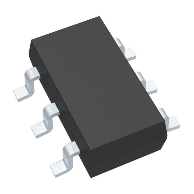
Package options and pin configuration for PL602-03SC-R
Package selection and pin allocation play a critical role in integration efficiency for timing devices such as the PL602-03SC-R. The device is delivered in two industry-standard surface-mount packages: 8-pin SOIC (3.90 mm width) and TSSOP. Both formats enable compatibility with automated pick-and-place lines, minimizing assembly variance and reducing manual intervention. The physical form factor addresses constraints for PCB density, with SOIC offering robust mechanical stability, while TSSOP provides tighter pitch for space-limited layouts. These options cater to both prototyping and volume production, facilitating rapid transitions from breadboard testing to final board assemblies.
The pin configuration of the PL602-03SC-R reflects established conventions for crystal oscillator modules, ensuring predictable electrical interfacing and simplifying schematic design. Pin 1 (CLK) delivers a defined output clock, characterized by low skew and sufficient drive strength for downstream digital circuits. Pin 2 (VDD) maintains operational integrity over recommended supply voltages, supporting decoupling practices that mitigate ripple and noise intrusion. Pin 3 (OE), equipped with an internal pull-up resistor, effectively defaults the device to active operation unless explicitly overridden. This eliminates the necessity for external bias components, reducing BOM complexity and avoiding inadvertent disablement due to open circuit conditions.
Pin 4 (XIN) and Pin 5 (XOUT) offer direct connection points for crystal load, accommodating frequency selection requirements. The implementation supports a wide range of crystal parameters, promoting interoperability while minimizing phase jitter. Pin 6 (N/C) conserves potential for future enhancements or cross-compatibility across derivative products without electrical compromise. Ground connections at Pins 7 and 8 provide dual anchor points for the substrate, which, through careful layout, improve EMC performance and signal integrity by optimizing return paths.
Practical application reveals that the internal OE pull-up is especially useful for adaptive board reuse strategies; circuits can be repurposed or adapted to legacy layouts without necessitating redesign for the enable signal. This characteristic expedites iterative development, with test builds reliably defaulting to functional output, streamlining system validation and reducing setup errors. When socketing is employed for rapid prototyping or qualification, pinout regularity ensures minimal adaptation overhead, fostering accelerated evaluation workflows.
A nuanced understanding of the device’s electrical abstraction yields improved PCB reliability. For instance, assigning ground pins at opposite ends counters cross-talk and reinforces current balancing. The physical separation of crystal input/output from power and digital signals furthers isolation, enhancing frequency stability. Integrating the PL602-03SC-R within multilayer boards leverages these principles, supporting high clock fidelity in complex embedded designs. This symmetry between package versatility and pin function exemplifies design-for-manufacturing philosophy, enabling robust deployment from concept to mass production and encouraging modular system frameworks where oscillator modules can be interchanged seamlessly.
Potential equivalent/replacement models for PL602-03SC-R
When responding to the obsolescence of the PL602-03SC-R clock oscillator, replacements must be narrowed by electrical and mechanical alignment with the original module. The core attributes underpinning successful migration include identical frequency coverage (48–100 MHz), CMOS-level output logic, and reliable 3.3V single-rail power compatibility. Selecting oscillators with low phase noise and jitter specifications is essential, as these metrics directly impact high-speed serial data performance and timing integrity in synchronous designs.
Identifying suitable substitutes begins with a focused scan of clock oscillator offerings from established vendors such as Microchip Technology, Texas Instruments, Renesas, and Silicon Labs. These suppliers maintain product families targeting precision clocking, frequently with pin-compatible packages and factory-programmed frequency options. Of particular concern is the attention to phase noise and rms jitter, where modern oscillator ICs leverage advanced crystal multiplication techniques and optimized noise filtering to drive sub-picosecond jitter floors, thereby safeguarding overall system signal quality.
Integration aspects deserve proper weighting. Solutions embedding crystal load capacitors within the package promote layout efficiency and mitigate PCB parasitics, reducing board tuning overhead and de-risking even minor redesigns. The availability of matched drive strengths ensures seamless interfacing with downstream gates or clock trees, eliminating signal integrity compromises. Over recent product lifecycles, cross-referencing datasheets for output symmetry, start-up time, and supply current has proven critical for fully characterizing drop-in viability—overlooking these second-order variables has frequently led to subtle timing bugs and compliance failures during certification.
Within advanced applications such as high-speed networking, industrial automation, or precision data acquisition, the marginal gains in jitter performance achieved by newer equivalent devices can yield disproportionate improvements in bit-error rates or ADC signal-to-noise ratios. Consequently, disciplined assessment against application-level constraints is warranted, rather than a superficial focus on headline parameters alone.
The obsolescence of a legacy clock source like the PL602-03SC-R also introduces an opportunity for system-level optimization. Leveraging newer oscillators’ support for enhanced features—such as wider frequency programmability, output enable/disabling logic, or micro-power standby functionality—enables downstream flexibility in circuit operation and power management, contributing to product robustness and lifecycle extension.
In sum, the migration process must triangulate parametric equivalence, package and layout continuity, and forward-compatibility with the evolving demands of timing-sensitive platforms. This approach not only mitigates risk during product refreshes but frequently reveals advantages unlocked by advancements in modern timing silicon.
Conclusion
The PL602-03SC-R from Microchip Technology exemplifies a refined clock oscillator designed to address the precision timing requirements prevalent in advanced electronic systems. Its core architecture centers on delivering exceptionally low phase noise across a broad frequency range, ensuring minimal signal distortion and highly reliable timing references. Oscillator outputs remain spectrally clean, primarily due to advanced waveform shaping and integrated noise suppression techniques. These features directly enhance data integrity in sensitive applications such as high-speed serial interfaces, communications equipment, and measurement instrumentation, fostering stability even under challenging operating environments.
The device’s integration of multiple functional blocks—including on-board voltage regulation and filtering—reduces dependence on external components and streamlines PCB layout. This systematic minimization of susceptibility to supply fluctuations or board-level interference enables designers to maintain consistent signal performance throughout the signal distribution network. Furthermore, compliance with international standards simplifies product certification cycles, accelerating time-to-market for designs requiring rigorous timing compliance.
Despite its robust technical profile, the PL602-03SC-R’s transition into an obsolete status prompts a strategic approach to component risk management. Direct replacements demand careful vetting for equivalent electrical characteristics, phase noise profiles, and interface compatibility. Experience in the field consistently demonstrates that comprehensive analysis of legacy oscillator parameters, paired with systematic evaluation of alternative suppliers, can forestall system-level timing issues and reduce unexpected design iterations.
Integrated feature sets, such as programmable output frequencies and selectable logic levels, yield practical versatility in mixed-signal environments where clock synchronization across diverse submodules is vital. Deploying the PL602-03SC-R in high-density board designs typically simplifies timing architectures while reducing overall BOM complexity. These engineering efficiencies translate directly into cost savings and enhanced long-term maintainability.
A nuanced appreciation of the oscillator’s design—particularly its emphasis on phase noise, jitter control, and electromagnetic compatibility—serves as a benchmark when assessing next-generation timing solutions. Rather than treating obsolescence as a liability, its technical legacy provides a framework for evaluating innovations in modern clock technology, helping to distinguish between genuine performance gains and marginal improvements. By internalizing these layered technical and operational insights, one can advance both immediate integration strategies and long-range component roadmaps with a high degree of confidence.