 >
>


Product Overview of MAX5500AGAP+T Series
The MAX5500AGAP+T series exemplifies advanced integration in multi-channel digital-to-analog conversion, blending high-resolution performance with optimized form factor and energy efficiency. At its core lies a 12-bit architecture, establishing a balance between granularity and dynamic range while maintaining manageable complexity in system design. The four-channel configuration provides parallel output control, beneficial for synchronized actuation in process automation, signal conditioning, or multi-axis motor control. Differential voltage-buffered outputs on each channel minimize susceptibility to noise and improve common-mode rejection, thereby enhancing output integrity in electromagnetically challenging environments.
The underlying circuit topology employs precision resistor networks and proprietary switching techniques to achieve consistent linearity and low glitch energy. These characteristics are vital in applications requiring stable output during rapid code transitions, such as programmable gain amplifiers or adaptive reference generators. The device’s low power profile, enabled by optimized biasing and CMOS process enhancements, directly supports remote and battery-powered systems where thermal dissipation must be controlled. Refinements in power consumption also enable broader deployment within distributed sensing platforms—where maintaining energy budgets is critical.
The 20-SSOP packaging addresses board layout challenges by offering dense pin mapping and reduced footprints. This facilitates integration into compact PCBs without compromising mechanical stability or solderability, especially during high-speed surface-mount assembly. The extended temperature range, spanning -40°C to +105°C, reflects deliberate engineering suitable for industrial ecosystems where operational continuity cannot be sacrificed to environmental stress. Such robustness allows deployment in outdoor enclosures, automotive modules, and factory floor instrumentation, often without additional thermal mitigation.
In practical deployment, rapid prototyping with the MAX5500AGAP+T consistently demonstrates stable DAC operation over large code sweeps—minimizing offset and drift even after extended runtime in temperature-cycled test chambers. Adaptive calibration routines can leverage the device’s predictable transfer function, and margin testing reveals resilience against supply variations and signal reflections. These real-world findings underscore the value of combining differential outputs and wide environmental tolerance.
The device’s scalability and channel independence inherently streamline system expansion and algorithmic control, enabling precision output staging, multi-point test equipment, and complex waveform synthesis. This modularity, paired with low-noise performance, positions the MAX5500AGAP+T not simply as a converter, but as a fundamental enabler for precision signal processing architectures in emerging automation and instrumentation contexts. Such features underscore a design philosophy where engineered simplicity delivers measurable reliability and application versatility.
Key Features of MAX5500AGAP+T Series
The MAX5500AGAP+T series is architected for applications demanding high-precision analog output and flexible signal adaptation. At its foundation, the chip integrates four 12-bit voltage-output DACs into a compact footprint, optimizing board real estate while maintaining channel independence. Each DAC provides a dedicated external negative amplifier input, a key distinction that enables flexible gain configuration for custom output ranges. This architecture supports remote sensing, improving system accuracy by allowing the amplifier feedback to compensate for voltage drops across PCB traces or connectors—a critical advantage in precision industrial or instrumentation deployments.
The device draws power from a single +5V rail, minimizing system complexity in mixed-supply environments. The supply current is highly optimized; typical operation requires only 0.85mA, a figure beneficial for dense multi-channel systems or battery-operated platforms. The inclusion of a shutdown mode, driving consumption down to 10μA (typ), extends applicability to power-constrained designs, such as remote sensors or portable calibration equipment, where consumption profiles directly impact operational longevity.
To enhance reliability, the MAX5500AGAP+T series implements a robust power-on reset circuit, clearing all DAC registers and analog outputs to zero on startup. This mechanism ensures deterministic system behavior, eliminating unpredictable output states at power application. Moreover, the device retains the last analog output states upon shutdown, enabling fast recovery and seamless continuation of previous system states—a behavior valuable in systems where output transients or disruptions must be minimized, such as in closed-loop control environments or process automation.
The device supports force-sense output connections, which, when combined with its user-accessible amplifier negative inputs, facilitate true remote voltage regulation at the point-of-load—even across temperature gradients and harness resistance. This force-sense topology reinforces output accuracy under real-world wiring constraints, a necessity in test and measurement infrastructure or distributed sensor arrays.
For digital communications, the MAX5500AGAP+T integrates a 3-wire serial interface compatible with industry-standard SPI, QSPI, and MICROWIRE protocols. This unified interface approach streamlines integration with prevalent microcontroller and FPGA platforms, reducing firmware complexity and leveraging existing codebases. The protocol’s structure permits both simultaneous and independent channel updates, aligning with throughput requirements in high-speed or multi-signal synthesis scenarios.
The device’s 12μs typical settling time supports both static and dynamic signal generation, including waveform synthesis and programmable biasing. Output bandwidth and channel update flexibility are adequate for applications such as arbitrary function generators or fine-grained actuator control. Furthermore, all digital logic inputs are compatible with both TTL and CMOS logic levels, promoting seamless adoption in mixed-voltage architectures and ensuring signal integrity in tightly coupled digital-analog mosaic designs.
Practical integration often emphasizes board-level grounding, especially with high-resolution DACs. The MAX5500AGAP+T mitigates coupled noise susceptibility through its low-drive logic and well-defined analog-digital partitioning. Configuring external amplifiers to leverage the available gain flexibility can optimize SNR and linearity for bespoke output requirements, especially when interfacing with variable loads or when minimizing total uncorrected error is a design priority.
Comparing the overall feature set and performance envelope, the series demonstrates a design philosophy favoring configurable precision and system-oriented power management over raw speed or fully integrated output drive. Its balanced offering is particularly advantageous in modular platforms where analog output channels must scale, respond rapidly to control domains, and coexist efficiently with diverse digital logic levels. The synthesis of force-sense topology, ultra-low shutdown current, and power-on reset capability fosters confidence in mission-critical or always-on architectures, where reliability and deterministic output matter most.
Applications and Engineering Scenarios for MAX5500AGAP+T Series
The MAX5500AGAP+T series demonstrates significant versatility in high-reliability industrial environments. At its core, the series integrates 8-bit digitally controlled voltage output with precision buffered analog drivers, supporting force-sense feedback architectures. These underlying mechanisms allow for accurate voltage sourcing and closed-loop error compensation, essential for multi-channel signal conditioning and instrumentation systems. The force-sense configuration enables dynamically adaptive gain and offset calibration, minimizing systematic errors from cable losses or input impedance fluctuations. In engineering workflows, this facilitates robust analog interfacing, particularly in architectures requiring remote actuation or calibrated sensing across distributed process control networks.
Implementation in industrial process control presents numerous benefits. Utilizing its programmable outputs, analog signals can be flexibly allocated for valve actuators, temperature regulators, and pressure sensors, supporting modular control strategies. The extended temperature endurance accommodates deployments in outdoor installations or manufacturing lines with variable thermal profiles. Integration with microprocessor-controlled platforms enables iterative offset and gain tuning, providing granular adaptability in equipment testing, calibration routines, and precision motion control. In these scenarios, the MAX5500AGAP+T series helps establish closed-loop feedback, enhancing control system stability and accelerating convergence toward target conditions.
Within automatic test equipment, the device’s low drift and RoHS compliance align with demanding quality assurance needs. Its multi-channel architecture simplifies synchronized test setups, supporting efficient batch analysis of sensor arrays or analog module assemblies. Configurability extends to remote industrial control, where long transmission lines typically introduce voltage drops and signal distortion; the force-sense topology compensates for these issues, ensuring accuracy at distant loads.
Practical experience highlights the importance of accurate voltage calibration when interfacing with high-resolution ADCs or sensitive actuators. Using the device’s feedback path, errors induced by environmental variability or aging components are suppressed in real time, maintaining calibration integrity without manual intervention. The buffered output design reduces crosstalk and load-induced transients, contributing to predictable multi-channel performance across complex workflows.
A core insight emerges regarding system scalability: leveraging the MAX5500AGAP+T series advances modularity and maintainability in distributed control platforms. By coupling digital control with adaptive analog correction, the device supports scalable infrastructure where nodes can autonomously manage calibration and signal integrity, reducing dependency on centralized intervention. This capability directly contributes to streamlined design cycles and reliable long-term operation in dynamic engineering contexts.
Electrical Characteristics and Performance of MAX5500AGAP+T Series
The MAX5500AGAP+T series embodies a robust architecture optimized for precision analog output in demanding signal chain applications. At its core, the 12-bit digital-to-analog conversion leverages finely tuned resistor string architectures and precision trimming during fabrication. This foundation delivers inherent monotonicity, with differential nonlinearity constrained within ±1.0 LSB, ensuring seamless transition and eliminating code errors that could introduce distortion in closed-loop control or instrumentation systems.
Integral nonlinearity, typically at ±0.25 LSB and capped at ±0.75 LSB for AGAP grades, reflects highly controlled process variations and meticulous error compensation schemes. These attributes guarantee that DAC output closely tracks the ideal transfer function, a critical requirement for accurate waveform synthesis and calibration-grade measurement systems. The true rail-to-rail output swing provides maximal signal utilization across the output range, straightforwardly interfacing with logic or analog subsystems without headroom constraints.
Dynamic specification further accentuates versatility. The output amplifier’s 0.6V/μs slew rate and 12μs settling time to within ±0.5 LSB (evaluated on a 5kΩ/100pF load) enable prompt response to rapid code transitions, even under capacitive loading prevalent in ADC-feedback or sample-and-hold architectures. Output integrity is preserved with controlled ringing and minimal overshoot, essential for maintaining low glitch energy in multi-channel synchronization scenarios.
Offset errors, constrained to ±3.5mV, are managed through laser trimming and precision offset cancellation topologies. This level of offset minimization is indispensable in applications like offsets for programmable power supplies or precision voltage references, where even minor deviations propagate as systemic gain errors. Notably, power-supply rejection at 100μV/V (typical for MAX5500) safeguards output stability amidst supply perturbations, ensuring noise immunity across mixed-signal environments characterized by digital switching artifacts.
Thermal stability is another pivotal layer. Both full-scale error and quiescent supply current demonstrate insensitivity to temperature fluctuations or varying loads. This minimizes recalibration intervals in field deployments, ultimately translating into resilient performance under diverse operational envelopes. Experienced design practice confirms that integrating DACs with such tightly governed electrical behavior streamlines qualification cycles and reduces failure modes related to drift or cross-coupling.
Real-world implementation benefits from compact form factor and low-power operation, directly supporting battery-powered instrumentation, process control, or remote acquisition modules. Developers also gain from layout flexibility—rail-to-rail outputs and well-suppressed offset error permit minimal external signal conditioning, reducing board space and bill of materials while enhancing long-term reliability.
This combination of precision, stability, and robust rail-to-rail architecture positions the MAX5500AGAP+T as a strong candidate wherever predictable, high-resolution analog control or synthesis is paramount. Particular care in device selection and board-level layout, such as tight analog ground referencing and attention to bypass capacitance, leverages its performance ceiling—especially in applications with high channel counts or mission-critical calibration requirements. These aspects collectively underscore the series' effectiveness for precision analog outputs within today’s interconnected and noise-sensitive system topologies.
Reference Inputs and Output Stage Details of MAX5500AGAP+T Series
The MAX5500AGAP+T series employs two distinct reference input channels—REFAB serving DACs A/B and REFCD connected to DACs C/D—enabling flexible, independent full-scale voltage settings. This dual-reference architecture streamlines multi-domain designs, allowing each DAC channel pair to operate under separate reference conditions. The reference input voltage accepts 0V up to (VDD – 1.4V), optimizing compatibility with a broad array of precision references and supporting tailored output dynamic ranges. Such versatility is particularly beneficial in mixed-signal control systems, where sensors or actuators often require disparate drive levels to achieve optimal performance.
Input impedance on each reference line follows a code-dependent profile. While the minimum is 10kΩ (guaranteed under all configurations), the impedance can extend to giga-ohm magnitudes depending on the DAC code and sourcing model. This behavior merits attention in reference selection and buffer design. Precision references, typified by the MAX6033, deliver optimal performance when operating with high source impedances that mirror the MAX5500AGAP+T’s typical conditions. Direct connection to a low-output-impedance reference stabilizes the reference node voltage, even when the impedance drops at certain codes due to internal DAC switching dynamics.
If the device enters shutdown, the reference inputs and output amplifiers transition to high-impedance states. This functional isolation eliminates load effects on shared or sensitive reference buses, safeguarding signal chain integrity during power-domain sleep intervals or hot-swapping scenarios. Implementations in precision measurement or process automation benefit in particular, as it prevents unintended reference voltage leakage and system-level drifting.
Each output amplifier includes a dedicated external negative input terminal. This structural detail opens pathways for gain programmability and sophisticated signal conditioning, extending far beyond unity gain configurations. By designing custom resistor networks or feedback loops, it is possible to set precise gain, offset, or summing behavior at each DAC output, crucial in environments requiring remote sensing, ground-referenced voltage adaption, or active loop compensation. An often-overlooked advantage is the accelerator effect on feedback-controlled installations, as direct access to the inverting input enables tight correction of distributed system errors.
The flexibility embedded in the reference and output stages produces a highly malleable DAC component. In advanced instrumentation, laboratory automation, and process control, these features encourage architectures where output scaling and impedance adaptation play central roles. A nuanced understanding of code-dependent impedance and shutdown isolation results in reference networks that remain stable and accurate under varying load and operational conditions. Integrated negative inputs on output stages further distinguish the MAX5500AGAP+T series, empowering designers to directly address nonstandard signal requirements and maximize overall system performance within constrained analog domains.
Power Management and Shutdown Capabilities in MAX5500AGAP+T Series
Power management in the MAX5500AGAP+T series integrates both hardware and software strategies, supporting scalable optimization of energy consumption in precision analog subsystems. Hardware-level control is achieved via the active-low power-down lockout (PDL) pin, which enables deterministic enforcement of shutdown policies, ensuring that voltage rails and related loads can be systematically deactivated by external controllers or fault detection logic. This hardware approach eliminates ambiguity and provides a failsafe mechanism in systems where unpredictable firmware states could otherwise leave circuits unintentionally powered, increasing reliability in critical environments.
Software-programmable shutdown supplements this hardware mechanism by allowing configurable power-state management through register access. This feature reduces the supply current down to 10μA while preserving both register configurations and DAC output codes. The state retention capability is instrumental for applications requiring immediate resumption of analog output post-wake, avoiding delay associated with reinitialization or recalibration routines. The architecture addresses challenges in low-power sensor nodes and industrial distributed control modules, where frequent transitions between operating and quiescent states must occur without data loss or excessive latency.
The design achieves a balance between rapid wake-up and power savings: transitioning out of shutdown incurs only a 15μs stabilization interval. This low wake-up latency supports applications demanding prompt response to real-time triggers, such as remote actuation circuits, feedback loop controls, or precision analog waveform synthesis under tight time budgets. The minimal downtime maximizes duty cycling opportunities without sacrificing output fidelity.
In practical PCB layouts, care is needed to properly de-glitch the PDL pin and shield associated traces to prevent inadvertent mode switching caused by transients or EMI. Additionally, sequencing routines must account for the brief inactivity interval following shutdown exit to guarantee subsequent analog outputs are valid. When integrating with microcontroller-based supervisory systems, leveraging the dual hardware-software shutdown pathways allows robust management schemes, such as automated sleep policies complemented by watchdog-enforced hardware overrides.
A critical insight emerges when considering long-term system reliability and energy scaling. By supporting parallel hardware and software control of shutdown states, the MAX5500AGAP+T offers a layered defense against energy leaks and state volatility, a necessity in increasingly complex industrial and remote sensor platforms. This multi-modal strategy enables not only minimal quiescent current draw but also robust recovery and deterministic resumption pathways—key for maintaining high availability without compromising on energy efficiency or operational integrity.
Serial Interface and Configuration Options in MAX5500AGAP+T Series
The MAX5500AGAP+T series incorporates a versatile serial interface engineered for seamless integration into a wide range of digital control architectures. Supporting SPI, QSPI, and MICROWIRE protocols, the device eliminates compatibility barriers and streamlines signal routing, particularly in dense multi-device environments. This protocol flexibility permits efficient configuration in both legacy and modern embedded platforms without significant firmware rework.
Data communication utilizes a rigorously structured 16-bit serial word, comprising 4 address/control bits and 12 data bits transmitted with the MSB first. The address/control segment facilitates granular targeting of specific internal registers and operational commands, enabling deterministic manipulation of output channels or system states. The separation of data and control in serial transmission bolsters reliability and permits precise batch operation scheduling within the host processor's main loop.
Double buffering is a foundational mechanism within the series, designed to optimize update latency and minimize output glitches. Incoming serial data first populates input registers, isolated from the output DAC latches. This structure allows pre-loading of multiple values across channels, poised for either individual or synchronous update triggers. Such capability is critical in instrumentation and closed-loop control, where simultaneous parameter shifts—such as coordinated bias adjustment or multi-channel calibration—must occur atomically to preserve system integrity.
The serial interface's active capability during power-down mode is a strategic feature, particularly for distributed systems or remote sensor nodes. This mechanism preserves communication pathways for configuration or diagnostic purposes, reducing the overall I/O bandwidth demands on the central controller. Embedded system experience indicates that this interface-level resilience ensures effective deployment in environments with stringent power cycling protocols, avoiding unnecessary wake events while maintaining supervisory access.
Augmenting configurability, the user-programmable logic output (UPO) and serial data output (DOUT) expand inter-device signaling and status tracking. UPO enables custom logic-driven output functionality, such as diagnostic flags or external enable signals, negating the need for additional GPIO multiplexing. DOUT is leveraged for daisy-chaining multiple DACs or for read-back operations, forming dynamic, scalable control networks. Seasoned integration scenarios reveal that this modular approach simplifies both hardware layout and software polling routines, leading to improved maintainability and fault tolerance.
Underlying these features is a robust design principle: tightly coupling layered serial access with application-centric configuration paths. The MAX5500AGAP+T series exemplifies not just protocol flexibility and operational efficiency, but also strategic resilience in complex embedded systems—manifested in power-conscious operation, precision update management, and scalable integration. This layered technical architecture delivers measurable benefits in environments demanding reliable, adaptive, and low-overhead digital-to-analog management.
Package, Environmental, and Reliability Aspects for MAX5500AGAP+T Series
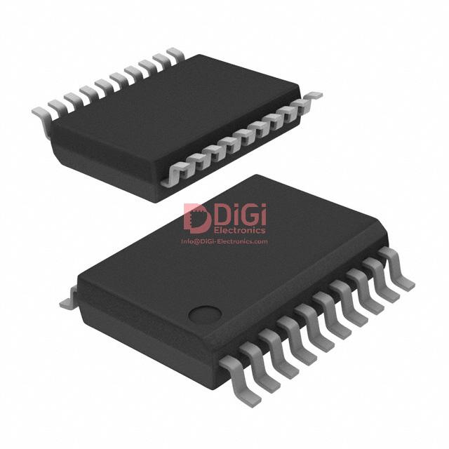
MAX5500AGAP+T utilizes the 20-SSOP package, engineered for streamlined integration in high-density surface-mount layouts. This package profile enables efficient use of board space and supports automated manufacturing processes, reducing assembly time and minimizing placement errors. The physical footprint balances thermal management demands with electrical isolation, optimizing both heat dissipation and signal integrity. The pin configuration enhances routing flexibility, facilitating complex multi-layer PCB designs and promoting compatibility with existing assembly infrastructure.
The device fulfills rigorous environmental criteria, performing reliably within the wide industrial temperature span of -40°C to +105°C. Such specification ensures stable analog performance under variable climate and operational stress, especially in environments where rapid temperature fluctuations or outdoor exposure are routine. Temperature tolerance extends not only to functional behavior but also to preservation of package integrity and solder joint reliability, mitigating risks associated with thermal cycling and mechanical stress.
MAX5500AGAP+T meets RoHS3 standards and is unaffected by REACH directives, streamlining material compliance for global deployment. Component selection conforms to hazardous material restrictions, avoiding requalification delays and facilitating acceptance in sectors with strict regulatory oversight. The series is classified as MSL 1, indicating unrestricted shelf life and negligible moisture sensitivity. This designation is critical during storage, transport, and prolonged inventory, eliminating concerns of latent reliability issues and supporting flexible supply chain practices.
Reliability considerations are embedded in both the package design and manufacturing processes. The MSL 1 rating ensures robustness through multiple reflow cycles without degradation, supporting design iterations and prototyping without elevated failure rates. Environmental resilience is especially relevant in industrial control, instrumentation, and telecommunication systems, where long-term operational continuity is non-negotiable. Past deployment in harsh field conditions has demonstrated stable performance, with minimal maintenance and downtime attributable to package-related failures.
From a system engineering perspective, MAX5500AGAP+T reduces risk in mission-critical applications by combining environmental hardening, compliance, and package reliability. Obsolescence management benefits from RoHS3/REACH immunity, and integration strategies leverage its compact SSOP format to maximize board real estate in dense modular designs. These factors converge to deliver consistent, sustainable long-term value and ease regulatory navigation, positioning the series as an optimal solution for designers prioritizing reliability, environmental conformity, and efficient layout integration.
Potential Equivalent/Replacement Models for MAX5500AGAP+T Series
A thorough assessment of equivalent and replacement options for the MAX5500AGAP+T series begins with understanding the fundamental parameters influencing device selection—namely, supply voltage ranges, accuracy specifications, and interface requirements. The MAX5500AGAP+T and its direct variant, the MAX5500BGAP+T, differ in their integral nonlinearity, with the AGAP+T offering standard accuracy and the BGAP+T achieving ±2 LSB INL; this grade is often necessary for precision-sensitive applications such as instrumentation or closed-loop control where cumulative error must remain minimal. In scenarios demanding enhanced accuracy, the pragmatic choice is to prioritize tighter nonlinearity, though a trade-off may arise in terms of cost or power consumption.
System voltage alignment is fundamental when integrating these DACs into mixed-signal architectures. The MAX5501AGAP+T and MAX5501BGAP+T are tailored for +3V operations, making them suitable for platforms constrained by lower voltage rails, such as battery-powered or portable devices. This adaptation not only ensures seamless electrical compatibility but also supports robust operation under constrained power budgets, reducing thermal stress and optimizing long-term reliability. Careful evaluation of voltage tolerance and startup conditions mitigates the risk of peripheral failures or erratic behavior, which is particularly relevant in high-uptime, fault-resistant deployments.
Device interface compatibility merits meticulous scrutiny, typically starting with the SPI or I²C connections. Variations in timing, voltage thresholds, and protocol support can introduce subtle mismatches, requiring engineers to validate electrical and logical characteristics via datasheet cross-referencing. Experience demonstrates that even minor discrepancies in digital interface design, such as clock polarity or data framing, can propagate integration errors that are difficult to debug post-deployment. Early prototyping and signal validation facilitate smooth migration when transitioning between equivalent models, streamlining the firmware adaptation process and minimizing unforeseen interoperability challenges.
From a deployment perspective, clear awareness of system-level trade-offs is essential. For designs where supply flexibility and precision must be harmonized, selection strategies should weigh voltage adaptability against cumulative linearity error; this multidimensional analysis often yields a preferred solution aligned with application-specific tolerances. Moreover, leveraging device variants within the same series reduces risk by maintaining consistent package footprints and pin assignments, thus expediting schematic-level changes and PCB updates. Evidence suggests that modular hardware revisions—where only the DAC variant is swapped—promote rapid iterations for custom accuracy and voltage requirements without introducing systemic uncertainties.
The distinction between incremental accuracy and supply compatibility should not be viewed as mere checklist items; they dynamically shape the functional landscape of embedded signal-generation subsystems. Robustness in design depends on a layered approach: first, verify core electrical requirements; second, align precision with application demands; lastly, address peripheral communication. Embedding these priorities within the selection process enhances not only technical compliance but also operational resilience in evolving engineering projects.
Conclusion
The MAX5500AGAP+T DAC series exhibits advanced configurability paired with low power consumption, targeting rigorous requirements within industrial and instrumentation environments. At its core, the device integrates four 12-bit channels, enabling fine control over analog signal outputs, critical for systems demanding high precision—such as motor controllers, sensor calibration interfaces, and automated test equipment. The architecture provides dynamic flexibility, including selectable internal or external reference modes. This ensures adaptability across varying stability requirements and signal integrity constraints, particularly when aligning output voltage ranges precisely with downstream circuitry or application-specific thresholds.
Deploying the MAX5500AGAP+T is further characterized by robust output stage options, with buffered and unbuffered configurations suited to different load scenarios. Buffered outputs accommodate applications where signal drive strength and low impedance loads are priorities, mitigating voltage sag and preserving waveform fidelity. Conversely, unbuffered operation supports minimal power dissipation, making it favorable in thermally constrained modules or portable instrumentation. Engineers benefit from seamless interfacing via efficient serial communication—most commonly SPI—allied to fast settling times. This combination allows rapid and deterministic analog updates, supporting high-speed feedback control loops and real-time response requirements in data acquisition or process automation.
Power management is optimized throughout, underscoring the series’ suitability for battery-powered designs and multi-node distributed systems. The low quiescent current profile not only extends operational life but also simplifies compliance with regulatory energy standards, enhancing deployment flexibility in greenfield projects and retrofit scenarios alike. Environmental robustness is complemented by alternative models within the series, facilitating straightforward design migration and minimizing lifecycle risks. These variants address extended temperature ranges and package options, aligning seamlessly with evolving procurement policies that prioritize component reliability and long-term availability.
Operational experience reveals distinct advantages in precision signal generation and adaptive calibration, supporting iterative tuning and system optimization with minimal external circuitry. Noise immunity and thermal stability have proven consistent across multiple deployment contexts, reinforcing design confidence when integrating into mission-critical subassemblies. The technical depth inherent in the MAX5500AGAP+T’s configuration set directly empowers iterative prototyping and field adjustments—contributing to agile process development that is increasingly demanded in competitive instrumentation markets. The device’s balance of performance, configurability, and environmental resilience positions it as a reliable cornerstone for engineers prioritizing both immediate feasibility and forward-compatible system architectures.