


Request Quote
(Ships tomorrow)
TS512IN Equivalent & Substitute Parts
Part Overview
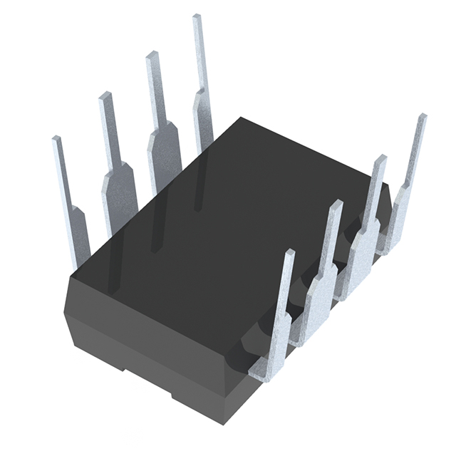
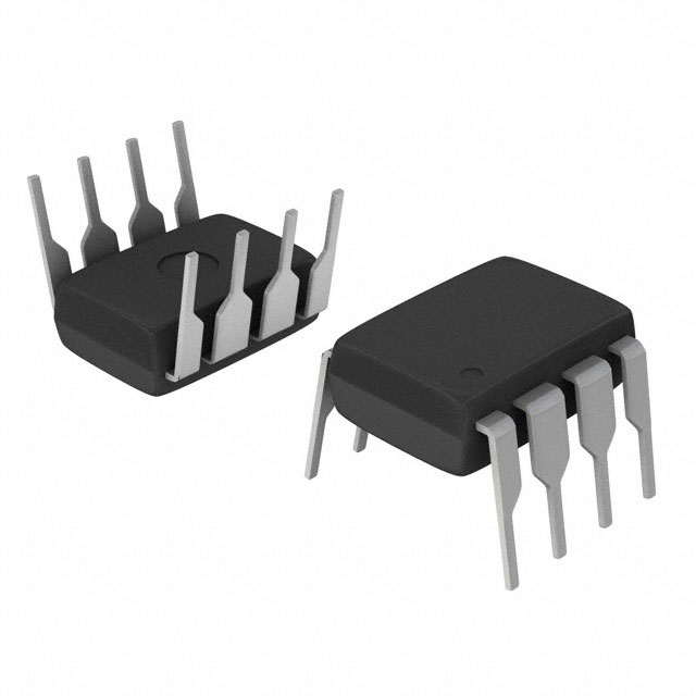
The TS512IN is a general-purpose operational amplifier manufactured by STMicroelectronics, configured as a dual-channel (2 circuit) device in an 8-Mini DIP through-hole package. This part is classified as obsolete, which necessitates identification of active equivalent and substitute components for new designs and ongoing production support. The TS512IN operates across a wide supply voltage range (3V to 30V) and is qualified to AEC-Q100 automotive standards, making it suitable for automotive and industrial applications requiring general-purpose amplification.
Substiute Parts
Key Parameters
| Parameter | Value | Unit |
|---|---|---|
| Manufacturer Part Number | TS512IN | — |
| Manufacturer | STMicroelectronics | — |
| Amplifier Type | General Purpose | — |
| Number of Circuits | 2 | — |
| Package / Case | 8-DIP (0.300", 7.62mm) | — |
| Mounting Type | Through Hole | — |
| Slew Rate | 1.5 | V/µs |
| Gain Bandwidth Product | 3 | MHz |
| Current - Input Bias | 50 | nA |
| Voltage - Input Offset | 500 | µV |
| Current - Supply | 500 | µA (x2 Channels) |
| Current - Output / Channel | 23 | mA |
| Voltage - Supply Span (Min) | 3 | V |
| Voltage - Supply Span (Max) | 30 | V |
| Operating Temperature | -40 to 125 | °C |
| Product Status | Obsolete | — |
| Grade | Automotive | — |
| Qualification | AEC-Q100 | — |
| RoHS Status | ROHS3 Compliant | — |
Substitute Part Grouping Explanation
Substitution of the TS512IN is determined by strict alignment of the following electrical and mechanical parameters:
Primary Substitution Criteria:
- Package type: 8-DIP (0.300", 7.62mm) through-hole configuration
- Number of circuits: 2 (dual-channel amplifier)
- Amplifier type: General Purpose
- Supply voltage compatibility: Minimum 3V to 30V operating range
- Mounting type: Through Hole
Secondary Compatibility Parameters:
- Slew rate: 1.5 V/µs (TS512IN baseline)
- Gain bandwidth product: 3 MHz (TS512IN baseline)
- Input bias current: 50 nA (TS512IN baseline)
- Input offset voltage: 500 µV (TS512IN baseline)
- Output current per channel: 23 mA (TS512IN baseline)
- Operating temperature range: -40°C to 125°C (TS512IN baseline)
Substitute parts are grouped based on whether they meet the primary criteria (package, circuit count, amplifier type, mounting) and how their secondary parameters compare to the TS512IN baseline. Parts with active product status are prioritized for new designs, while parts with obsolete or "Not For New Designs" status are noted accordingly.
Parameter Comparison
| Parameter | TS512IN | AD708JNZ | LT1013CN8#PBF | LT1013DN8#PBF | NJM3404AD | NJM4556AD | OP249GPZ |
|---|---|---|---|---|---|---|---|
| Manufacturer | STMicroelectronics | Analog Devices Inc. | Analog Devices Inc. | Analog Devices Inc. | Nisshinbo Micro Devices Inc. | Nisshinbo Micro Devices Inc. | Analog Devices Inc. |
| Product Status | Obsolete | Active | Active | Active | Active | Not For New Designs | Active |
| Amplifier Type | General Purpose | General Purpose | General Purpose | General Purpose | General Purpose | General Purpose | J-FET |
| Number of Circuits | 2 | 2 | 2 | 2 | 2 | 2 | 2 |
| Package / Case | 8-DIP (0.300", 7.62mm) | 8-DIP (0.300", 7.62mm) | 8-DIP (0.300", 7.62mm) | 8-DIP (0.300", 7.62mm) | 8-DIP (0.300", 7.62mm) | 8-DIP (0.300", 7.62mm) | 8-DIP (0.300", 7.62mm) |
| Mounting Type | Through Hole | Through Hole | Through Hole | Through Hole | Through Hole | Through Hole | Through Hole |
| Slew Rate (V/µs) | 1.5 | 0.3 | 0.4 | 0.4 | 1.2 | 3 | 22 |
| Gain Bandwidth Product (MHz) | 3 | 0.9 | 1 | 1 | 1.2 | 8 | 4.7 |
| Current - Input Bias (nA) | 50 | 1 | 15 | 15 | 70 | 50 | 0.03 |
| Voltage - Input Offset (µV) | 500 | 30 | 60 | 60 | 2000 | 500 | 400 |
| Current - Supply (mA) | 0.5 | 4.5 | 0.35 | 0.35 | 2 | 8 | 5.6 |
| Current - Output / Channel (mA) | 23 | — | 20 | 20 | 30 | 70 | 36 |
| Voltage - Supply Span (Min) | 3 V | 6 V | 4 V | 4 V | 4 V | 4 V | 9 V |
| Voltage - Supply Span (Max) | 30 V | 36 V | 44 V | 44 V | 36 V | 36 V | 36 V |
| Operating Temperature (°C) | -40 to 125 | 0 to 70 | 0 to 70 | 0 to 70 | -40 to 85 | -40 to 85 | -40 to 85 |
| RoHS Status | ROHS3 Compliant | ROHS3 Compliant | ROHS3 Compliant | ROHS3 Compliant | RoHS Compliant | RoHS Compliant | ROHS3 Compliant |
Engineering Selection Recommendations
Primary Substitutes for Active Production:
The LT1013CN8#PBF and LT1013DN8#PBF (Analog Devices Inc., LT® series) are the preferred active substitutes for the TS512IN. Both parts maintain active product status, are ROHS3 compliant, and provide identical dual-channel general-purpose amplifier functionality in the 8-DIP through-hole package. The LT1013 series offers extended maximum supply voltage (44V versus 30V) and lower supply current (350µA versus 500µA), providing improved performance margins. Operating temperature range is reduced to 0°C to 70°C, which may require evaluation for automotive applications requiring the full -40°C to 125°C range of the TS512IN.
The NJM3404AD (Nisshinbo Micro Devices Inc.) is an active alternative that maintains the -40°C to 85°C operating temperature range and automotive-grade compatibility. This part exhibits higher input offset voltage (2mV versus 500µV) and input bias current (70nA versus 50nA), but provides comparable slew rate (1.2V/µs) and gain bandwidth product (1.2MHz).
Secondary Substitutes:
The AD708JNZ (Analog Devices Inc.) is active but exhibits reduced performance in slew rate (0.3V/µs) and gain bandwidth product (0.9MHz) compared to the TS512IN. Minimum supply voltage requirement is 6V, which exceeds the TS512IN's 3V minimum. Operating temperature is limited to 0°C to 70°C.
The NJM4556AD (Nisshinbo Micro Devices Inc.) carries "Not For New Designs" status and should not be selected for new applications. This part is retained in the substitute list due to its presence in the original TS512IN substitute specification.
The OP249GPZ (Analog Devices Inc.) is a J-FET amplifier type, fundamentally different from the general-purpose bipolar design of the TS512IN. While it maintains active status and the 8-DIP package, the J-FET architecture introduces different input bias current characteristics (30pA versus 50nA) and requires minimum 9V supply voltage. This part is suitable only for applications where J-FET input characteristics are specifically required.
Compliance Considerations:
All recommended active substitutes maintain ROHS3 compliance and REACH unaffected status, consistent with the TS512IN. The LT1013 series and NJM3404AD are preferred for new designs requiring continuation of the TS512IN functionality.
Frequently Asked Questions (FAQ)
Q: Can the LT1013CN8#PBF directly replace the TS512IN in existing designs?
A: The LT1013CN8#PBF is mechanically and functionally compatible as a direct replacement in the 8-DIP through-hole package. However, the operating temperature range is reduced from -40°C to 125°C (TS512IN) to 0°C to 70°C (LT1013CN8#PBF). Applications requiring operation below 0°C or above 70°C must use the NJM3404AD or evaluate the design for temperature-dependent performance changes.
Q: What is the difference between LT1013CN8#PBF and LT1013DN8#PBF?
A: Both parts are electrically identical with the same electrical specifications. The difference lies in the temperature grade designation (C-grade versus D-grade), which affects the operating temperature range and qualification testing. Both are active products suitable for new designs.
Q: Why is the OP249GPZ listed as a substitute if it is a J-FET amplifier?
A: The OP249GPZ is included because it was specified in the original TS512IN substitute list. However, the J-FET architecture represents a different amplifier topology with distinct input bias current characteristics (30pA versus 50nA). Selection of the OP249GPZ should be limited to applications where J-FET input characteristics provide specific design advantages.
Q: Is the NJM4556AD suitable for new designs?
A: No. The NJM4556AD carries "Not For New Designs" product status. While it remains available in inventory, it should not be selected for new applications. Use the LT1013 series or NJM3404AD for new designs.
Q: What are the key electrical differences between the TS512IN and its active substitutes?
A: The primary differences are slew rate (TS512IN: 1.5V/µs; LT1013: 0.4V/µs; NJM3404AD: 1.2V/µs), gain bandwidth product (TS512IN: 3MHz; LT1013: 1MHz; NJM3404AD: 1.2MHz), and operating temperature range (TS512IN: -40°C to 125°C; LT1013: 0°C to 70°C; NJM3404AD: -40°C to 85°C). Applications sensitive to slew rate or bandwidth performance must evaluate these differences.
Q: Can the TS512IN be used in applications requiring 3V minimum supply voltage?
A: Yes. The TS512IN specifies 3V minimum supply voltage. However, most active substitutes (LT1013, NJM3404AD, NJM4556AD) require minimum 4V supply voltage. The AD708JNZ requires 6V minimum. Applications with 3V to 4V supply rails must retain the TS512IN or evaluate alternative part families.
Q: Are all substitute parts RoHS compliant?
A: Yes. All listed substitute parts are RoHS compliant (either ROHS3 or RoHS compliant status). The TS512IN is ROHS3 compliant, and all substitutes maintain equivalent or superior compliance status.
Q: What is the significance of the 8-DIP package specification?
A: The 8-DIP (0.300", 7.62mm) package is a through-hole configuration with 0.3-inch row spacing and 7.62mm body width. All listed substitutes use identical package dimensions, ensuring mechanical compatibility with existing printed circuit board layouts and socket configurations. No PCB redesign is required for package compatibility.
Alternative Parts

SJ6012L2TP
Littelfuse Inc.
6 Alternative Parts

JMK107BBJ476MA-RE
Taiyo Yuden
10 Alternative Parts

GMK107BBJ475MA-T
Taiyo Yuden
5 Alternative Parts
SJ6020N2ARP
Littelfuse Inc.
3 Alternative Parts
SJ6025R2ATP
Littelfuse Inc.
4 Alternative Parts

2474-05L
API Delevan Inc.
1 Alternative Parts

4590R-684K
API Delevan Inc.
1 Alternative Parts

CM6560R-334
API Delevan Inc.
1 Alternative Parts

CM6460-104
API Delevan Inc.
1 Alternative Parts

5526-12
API Delevan Inc.
1 Alternative Parts