


Request Quote
(Ships tomorrow)
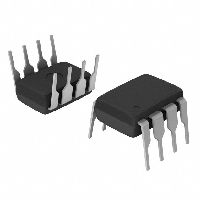
TS393CD C3G Equivalent & Substitute Parts
Part Overview
The TS393CD C3G is a dual-channel general-purpose comparator manufactured by Taiwan Semiconductor Corporation in 8-DIP through-hole packaging. This linear integrated circuit operates across a wide supply voltage range of 2V to 36V (single supply) or ±1V to ±18V (dual supply), making it suitable for diverse analog signal comparison applications. The device is currently in active production status with 16,200 units in stock inventory.
Substitute parts become necessary when the TS393CD C3G reaches end-of-life status, when specific packaging requirements differ from the original design, or when alternative sourcing is required to meet supply chain objectives. The parts listed below maintain functional equivalence within defined electrical and mechanical parameters.
Substiute Parts
Key Parameters
| Parameter | Value | Unit |
|---|---|---|
| Number of Elements | 2 | Channels |
| Output Type | CMOS, DTL, ECL, MOS, TTL | Logic Family |
| Voltage - Supply, Single/Dual (±) | 2V ~ 36V, ±1V ~ 18V | V |
| Voltage - Input Offset (Max) | 2mV @ 5V | mV |
| Current - Input Bias (Max) | 0.025µA | µA |
| Current - Output (Typ) | 16mA @ 5V | mA |
| Current - Quiescent (Max) | 1mA | mA |
| Operating Temperature | 0°C ~ 70°C | °C |
| Package / Case | 8-DIP (0.309", 7.87mm) | Through Hole |
| RoHS Status | ROHS3 Compliant | Certification |
| Moisture Sensitivity Level (MSL) | 1 (Unlimited) | Classification |
Substitute Part Grouping Explanation
Substitution eligibility for the TS393CD C3G is determined by the following critical parameters:
Primary Substitution Criteria:
- Dual-channel (2 elements) comparator architecture
- General-purpose comparator classification
- Compatible output logic families (CMOS, DTL, ECL, MOS, TTL)
- Supply voltage range overlap with original specification
- Through-hole or surface-mount packaging compatibility with circuit board design
Secondary Compatibility Factors:
- Input offset voltage performance
- Input bias current specifications
- Output current drive capability
- Quiescent current consumption
- Operating temperature range coverage
- RoHS3 compliance and MSL rating
The substitute parts identified below meet the primary substitution criteria. The MAX922EPA+ maintains through-hole 8-DIP packaging identical to the original part. The SC2903VDR2G provides functional equivalence in surface-mount 8-SOIC packaging for designs requiring alternative form factors.
Parameter Comparison
| Parameter | TS393CD C3G | MAX922EPA+ | SC2903VDR2G |
|---|---|---|---|
| Manufacturer | Taiwan Semiconductor Corporation | Analog Devices Inc./Maxim Integrated | onsemi |
| Number of Elements | 2 | 2 | 2 |
| Output Type | CMOS, DTL, ECL, MOS, TTL | CMOS, TTL | CMOS, DTL, ECL, MOS, TTL |
| Voltage - Supply, Single/Dual (±) | 2V ~ 36V, ±1V ~ 18V | 2.5V ~ 11V, ±1.25V ~ 5.5V | 2V ~ 36V |
| Voltage - Input Offset (Max) | 2mV @ 5V | 10mV @ 5V | Not specified |
| Current - Input Bias (Max) | 0.025µA | Not specified | Not specified |
| Current - Output (Typ) | 16mA @ 5V | 50mA | 20mA |
| Current - Quiescent (Max) | 1mA | 5µA | Not specified |
| Operating Temperature | 0°C ~ 70°C | -40°C ~ 85°C | Not specified |
| Package / Case | 8-DIP (0.309", 7.87mm) | 8-DIP (0.300", 7.62mm) | 8-SOIC (0.154", 3.90mm Width) |
| Mounting Type | Through Hole | Through Hole | Surface Mount |
| Product Status | Active | Active | Obsolete |
| RoHS Status | ROHS3 Compliant | ROHS3 Compliant | ROHS3 Compliant |
| MSL Rating | 1 (Unlimited) | 1 (Unlimited) | 1 (Unlimited) |
Engineering Selection Recommendations
MAX922EPA+ Selection Criteria:
The MAX922EPA+ is suitable as a direct substitute when through-hole 8-DIP packaging is required and the application operates within the reduced supply voltage range of 2.5V to 11V (single supply) or ±1.25V to ±5.5V (dual supply). This part is currently in active production status with 2,712 units in stock. The MAX922EPA+ exhibits higher output current capability (50mA typical) compared to the TS393CD C3G (16mA typical), which may provide improved drive capability for certain load conditions. The extended operating temperature range (-40°C to 85°C) accommodates industrial and automotive applications beyond the original part's 0°C to 70°C specification. Both parts maintain ROHS3 compliance and MSL 1 rating. The input offset voltage specification of 10mV at 5V is less stringent than the TS393CD C3G at 2mV, which may impact precision analog applications requiring tight offset tolerance.
SC2903VDR2G Selection Criteria:
The SC2903VDR2G provides functional equivalence in surface-mount 8-SOIC packaging for designs requiring alternative form factors or higher component density. This part maintains the full supply voltage range of 2V to 36V (single supply) matching the TS393CD C3G specification. However, the SC2903VDR2G is classified as obsolete product status, indicating discontinued manufacturing. Current inventory is limited to 796 units. This part carries AEC-Q100 automotive qualification and is suitable for automotive-grade applications. The SC2903VDR2G is appropriate only for new designs where surface-mount packaging is mandatory and long-term supply chain continuity is not a primary concern.
Compliance and Certification:
All three parts maintain ROHS3 compliance and MSL 1 (unlimited moisture sensitivity) rating, ensuring compatibility with modern manufacturing processes and storage requirements. All parts carry EAR99 export classification and are REACH unaffected.
Frequently Asked Questions (FAQ)
Q: Can the MAX922EPA+ replace the TS393CD C3G in all applications?
A: The MAX922EPA+ is functionally equivalent for applications operating within its reduced supply voltage range of 2.5V to 11V (single supply) or ±1.25V to ±5.5V (dual supply). Applications requiring the full 2V to 36V supply range of the TS393CD C3G cannot use the MAX922EPA+ without circuit redesign. The MAX922EPA+ is suitable for standard 5V and 3.3V logic systems.
Q: What are the packaging differences between these parts?
A: The TS393CD C3G and MAX922EPA+ both use 8-DIP through-hole packaging with nearly identical dimensions (0.309" vs 0.300" width), making them mechanically interchangeable on standard printed circuit boards with 0.1" pitch DIP sockets. The SC2903VDR2G uses 8-SOIC surface-mount packaging (0.154" width) and requires different PCB footprints and soldering processes.
Q: Why is the SC2903VDR2G listed as obsolete?
A: The SC2903VDR2G is classified as obsolete product status by the manufacturer, indicating discontinued production. While current inventory of 796 units is available, this part should not be selected for new designs requiring long-term component availability or future production runs.
Q: How do the electrical specifications differ between these parts?
A: The TS393CD C3G specifies 2mV maximum input offset voltage at 5V, while the MAX922EPA+ specifies 10mV, representing a 5x difference in offset accuracy. The MAX922EPA+ provides higher output current (50mA typical) compared to the TS393CD C3G (16mA typical). The TS393CD C3G specifies lower quiescent current (1mA maximum) compared to the MAX922EPA+ (5µA maximum). These differences affect precision, drive capability, and power consumption characteristics.
Q: Are all parts RoHS3 compliant?
A: Yes, all three parts (TS393CD C3G, MAX922EPA+, and SC2903VDR2G) are ROHS3 compliant with MSL 1 (unlimited) moisture sensitivity rating, meeting current environmental and manufacturing standards.
Q: Which part should be selected for automotive applications?
A: The SC2903VDR2G carries AEC-Q100 automotive qualification, making it the specified choice for automotive-grade applications. However, its obsolete status limits suitability for new designs. The MAX922EPA+ with extended operating temperature range (-40°C to 85°C) may be acceptable for automotive applications not requiring formal AEC-Q100 qualification, subject to design review and validation.
Q: What is the impact of different output current specifications?
A: The MAX922EPA+ (50mA typical output current) provides greater drive capability than the TS393CD C3G (16mA typical). Applications with high-impedance loads or requiring direct logic level switching may benefit from the increased output current. Applications with low-impedance loads or current-limited designs should verify that the higher output current does not introduce unintended circuit behavior.
Alternative Parts

SJ6012L2TP
Littelfuse Inc.
6 Alternative Parts

JMK107BBJ476MA-RE
Taiyo Yuden
10 Alternative Parts

GMK107BBJ475MA-T
Taiyo Yuden
5 Alternative Parts
SJ6020N2ARP
Littelfuse Inc.
3 Alternative Parts
SJ6025R2ATP
Littelfuse Inc.
4 Alternative Parts

2474-05L
API Delevan Inc.
1 Alternative Parts

4590R-684K
API Delevan Inc.
1 Alternative Parts

CM6560R-334
API Delevan Inc.
1 Alternative Parts

CM6460-104
API Delevan Inc.
1 Alternative Parts

5526-12
API Delevan Inc.
1 Alternative Parts