


Request Quote
(Ships tomorrow)
TLC3548CDW Equivalent & Substitute Parts
Part Overview
The TLC3548CDW is a 14-bit Analog to Digital Converter (ADC) manufactured by Texas Instruments, designed for data acquisition applications requiring moderate resolution and sampling rates. This device features a Successive Approximation Register (SAR) architecture with configurable input options (4 or 8 channels) and supports both pseudo-differential and single-ended input types. The TLC3548CDW is classified as Last Time Buy, indicating end-of-life status. Identifying equivalent and substitute parts is necessary to ensure continued design support, maintain supply chain continuity, and evaluate alternative solutions for new designs or production transitions.
Substiute Parts
Key Parameters
| Parameter | Value |
|---|---|
| Manufacturer Part Number | TLC3548CDW |
| Manufacturer | Texas Instruments |
| Category | Data Acquisition |
| Number of Bits | 14 |
| Sampling Rate (Per Second) | 200k |
| Number of Inputs | 4, 8 |
| Input Type | Pseudo-Differential, Single Ended |
| Data Interface | SPI |
| Architecture | SAR |
| Reference Type | External, Internal |
| Voltage - Supply, Analog | 5V |
| Voltage - Supply, Digital | 2.7V ~ 5.5V |
| Operating Temperature | 0°C ~ 70°C |
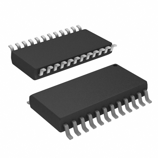
| Package / Case | 24-SOIC (0.295", 7.50mm Width) |
| Mounting Type | Surface Mount |
| Product Status | Last Time Buy |
| RoHS Status | ROHS3 Compliant |
Substitute Part Grouping Explanation
Substitution of the TLC3548CDW is determined by the following critical parameters:
Core Functional Parameters:
- Architecture (SAR)
- Data Interface (SPI)
- Number of A/D Converters (1)
- Configuration (MUX-S/H-ADC)
Electrical Compatibility Parameters:
- Supply voltage ranges (analog and digital)
- Operating temperature range
- Reference type capability
Physical Compatibility Parameters:
- Package type and pin count
- Mounting type (Surface Mount)
The ADS7951SDBTR qualifies as a substitute based on shared SAR architecture, SPI interface, single A/D converter configuration, and surface mount packaging. However, differences exist in resolution (12-bit vs. 14-bit), sampling rate (1M vs. 200k), input channel count (8 vs. 4/8), and input type support (single-ended only vs. pseudo-differential and single-ended).
Parameter Comparison
| Parameter | TLC3548CDW | ADS7951SDBTR |
|---|---|---|
| Manufacturer | Texas Instruments | Texas Instruments |
| Category | Data Acquisition | Data Acquisition |
| Number of Bits | 14 | 12 |
| Sampling Rate (Per Second) | 200k | 1M |
| Number of Inputs | 4, 8 | 8 |
| Input Type | Pseudo-Differential, Single Ended | Single Ended |
| Data Interface | SPI | SPI |
| Configuration | MUX-S/H-ADC | MUX-S/H-ADC |
| Number of A/D Converters | 1 | 1 |
| Architecture | SAR | SAR |
| Reference Type | External, Internal | External |
| Voltage - Supply, Analog | 5V | 2.7V ~ 5.25V |
| Voltage - Supply, Digital | 2.7V ~ 5.5V | 1.7V ~ 5.25V |
| Operating Temperature | 0°C ~ 70°C | -40°C ~ 125°C |
| Package / Case | 24-SOIC | 30-TSSOP |
| Mounting Type | Surface Mount | Surface Mount |
| Product Status | Last Time Buy | Active |
| RoHS Status | ROHS3 Compliant | ROHS3 Compliant |
Engineering Selection Recommendations
The ADS7951SDBTR is an active product from Texas Instruments and represents a viable alternative for designs transitioning away from the Last Time Buy TLC3548CDW. Both devices maintain ROHS3 compliance and are manufactured by the same supplier, ensuring consistent quality and support standards.
Selection of the ADS7951SDBTR requires evaluation of the following trade-offs:
Resolution Trade-off: The ADS7951SDBTR provides 12-bit resolution compared to the TLC3548CDW's 14-bit resolution. Applications requiring the full 14-bit precision of the original device may not be suitable for direct substitution.
Sampling Rate Advantage: The ADS7951SDBTR operates at 1M samples per second, providing a 5x increase over the TLC3548CDW's 200k samples per second. This enables higher-speed data acquisition applications.
Input Configuration: The ADS7951SDBTR supports 8 single-ended inputs exclusively. The TLC3548CDW supports both 4 and 8 channel configurations with pseudo-differential and single-ended input types. Designs requiring pseudo-differential inputs cannot use the ADS7951SDBTR as a direct substitute.
Package Consideration: The ADS7951SDBTR uses a 30-TSSOP package compared to the TLC3548CDW's 24-SOIC package. PCB layout modifications are required for physical substitution.
Temperature Range: The ADS7951SDBTR supports -40°C to 125°C operation, extending the lower and upper temperature limits beyond the TLC3548CDW's 0°C to 70°C range.
Reference Type: The ADS7951SDBTR supports external reference only, while the TLC3548CDW supports both external and internal references. Designs relying on internal reference capability require circuit redesign.
Frequently Asked Questions (FAQ)
Q: Can the ADS7951SDBTR directly replace the TLC3548CDW in existing designs?
A: Direct replacement is not recommended without design review. While both devices share SAR architecture and SPI interface, differences in resolution, input types, package, and reference capability require circuit and PCB modifications.
Q: What is the primary reason to consider the ADS7951SDBTR as an alternative?
A: The TLC3548CDW is Last Time Buy status. The ADS7951SDBTR is an active product from the same manufacturer, providing continued supply availability and long-term support for new designs or production transitions.
Q: Does the ADS7951SDBTR support pseudo-differential inputs?
A: No. The ADS7951SDBTR supports single-ended inputs only. The TLC3548CDW supports both pseudo-differential and single-ended input types. Applications requiring pseudo-differential input capability cannot use the ADS7951SDBTR.
Q: What are the package differences between these devices?
A: The TLC3548CDW uses a 24-SOIC package (0.295" width, 7.50mm). The ADS7951SDBTR uses a 30-TSSOP package (0.173" width, 4.40mm). PCB layout and footprint modifications are required for physical substitution.
Q: How do the resolution specifications compare?
A: The TLC3548CDW provides 14-bit resolution. The ADS7951SDBTR provides 12-bit resolution. Applications requiring 14-bit precision may experience reduced measurement accuracy with the substitute device.
Q: Are both devices RoHS compliant?
A: Yes. Both the TLC3548CDW and ADS7951SDBTR are ROHS3 compliant, meeting environmental and regulatory requirements for electronic components.
Q: What is the sampling rate difference?
A: The TLC3548CDW samples at 200k samples per second. The ADS7951SDBTR samples at 1M samples per second, providing 5x faster data acquisition capability.
Q: Does the ADS7951SDBTR support internal reference?
A: No. The ADS7951SDBTR supports external reference only. The TLC3548CDW supports both external and internal reference types. Designs using internal reference require external reference circuit implementation.
Q: What is the operating temperature range for each device?
A: The TLC3548CDW operates from 0°C to 70°C. The ADS7951SDBTR operates from -40°C to 125°C, providing extended temperature range capability for industrial and automotive applications.
Alternative Parts

SJ6012L2TP
Littelfuse Inc.
6 Alternative Parts

JMK107BBJ476MA-RE
Taiyo Yuden
10 Alternative Parts

GMK107BBJ475MA-T
Taiyo Yuden
5 Alternative Parts
SJ6020N2ARP
Littelfuse Inc.
3 Alternative Parts
SJ6025R2ATP
Littelfuse Inc.
4 Alternative Parts

2474-05L
API Delevan Inc.
1 Alternative Parts

4590R-684K
API Delevan Inc.
1 Alternative Parts

CM6560R-334
API Delevan Inc.
1 Alternative Parts

CM6460-104
API Delevan Inc.
1 Alternative Parts

5526-12
API Delevan Inc.
1 Alternative Parts