


Request Quote
(Ships tomorrow)
STW35N65DM2 Equivalent & Substitute Parts
Part Overview
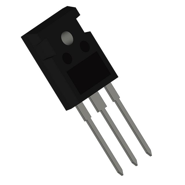
The STW35N65DM2 is an N-Channel MOSFET manufactured by STMicroelectronics, rated for 650V drain-to-source voltage with 32A continuous drain current at 25°C. This device is housed in a TO-247-3 through-hole package and is designed for high-voltage switching applications. The part is currently Active in product status and RoHS3 compliant.
Substitute parts are identified when equivalent electrical performance can be achieved within the specified parameter ranges while maintaining the same package type and mounting configuration. The following substitute devices meet the core electrical and mechanical requirements for direct replacement in applications where the STW35N65DM2 is specified.
Substiute Parts
Key Parameters
| Parameter | Value | Unit |
|---|---|---|
| Drain to Source Voltage (Vdss) | 650 | V |
| Continuous Drain Current (Id) @ 25°C | 32 | A |
| On-State Resistance (Rds On) @ 16A, 10V | 110 | mOhm |
| Gate Threshold Voltage (Vgs(th)) @ 250µA | 5 | V |
| Gate Charge (Qg) @ 10V | 56.3 | nC |
| Power Dissipation (Max) | 250 | W |
| Operating Temperature Range | -55 to 150 | °C |
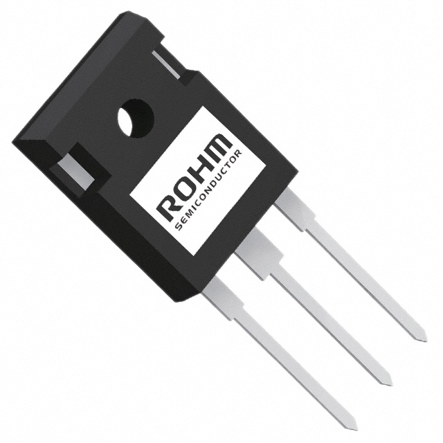
| Package Type | TO-247-3 | — |
| Mounting Type | Through Hole | — |
| Technology | MOSFET (Metal Oxide) | — |
Substitute Part Grouping Explanation
Substitute parts for the STW35N65DM2 are selected based on the following criteria:
Primary Electrical Parameters:
- Drain-to-source voltage (Vdss) rating of 650V or higher
- Continuous drain current (Id) capability of 32A or greater at 25°C
- On-state resistance (Rds On) within acceptable operating margins
- Gate threshold voltage (Vgs(th)) compatibility at specified test conditions
- Operating temperature range spanning -55°C to 150°C or higher
Mechanical & Package Requirements:
- Through-hole mounting configuration
- TO-247-3 or equivalent package footprint
- RoHS3 compliance
- REACH unaffected status
Technology Considerations:
- Silicon-based MOSFET technology (standard Metal Oxide Semiconductor)
- Silicon Carbide (SiCFET) technology with equivalent electrical performance
Substitutes are grouped into two categories: direct silicon MOSFET replacements and silicon carbide alternatives. Each substitute maintains compatibility with the original part's electrical specifications and package requirements.
Parameter Comparison
| Parameter | STW35N65DM2 (Main) | FCH110N65F-F155 | FCH104N60F | SCT3080ALGC11 |
|---|---|---|---|---|
| Manufacturer | STMicroelectronics | Fairchild Semiconductor | onsemi | Rohm Semiconductor |
| Vdss (V) | 650 | 650 | 600 | 650 |
| Id @ 25°C (A) | 32 | 35 | 37 | 30 |
| Rds On @ Vgs, Id (mOhm) | 110 @ 10V, 16A | 110 @ 10V, 17.5A | 104 @ 10V, 18.5A | 104 @ 18V, 10A |
| Vgs(th) @ Id (V) | 5 @ 250µA | 5 @ 3.5mA | 5 @ 250µA | 5.6 @ 5mA |
| Gate Charge Qg @ Vgs (nC) | 56.3 @ 10V | 145 @ 10V | 139 @ 10V | 48 @ 18V |
| Power Dissipation (W) | 250 | 357 | 357 | 134 |
| Operating Temperature (°C) | -55 to 150 | -55 to 150 | -55 to 150 | -55 to 175 |
| Package | TO-247-3 | TO-247-3 | TO-247-3 | TO-247N |
| Technology | MOSFET | MOSFET | MOSFET | SiCFET |
| Product Status | Active | Active | Not For New Designs | Active |
| RoHS3 Compliance | Yes | Not specified | Yes | Yes |
Engineering Selection Recommendations
FCH110N65F-F155 (Fairchild Semiconductor)
This substitute provides the closest electrical match to the STW35N65DM2. Both devices share identical Vdss (650V) and Rds On (110 mOhm) specifications. The FCH110N65F-F155 offers higher continuous drain current (35A vs. 32A) and increased power dissipation capability (357W vs. 250W). The device maintains Active product status and operates across the same temperature range. Gate charge is higher (145 nC vs. 56.3 nC), which may affect switching speed in high-frequency applications. This part is suitable for direct replacement in applications where the additional current and power handling capacity do not create thermal or circuit design conflicts.
FCH104N60F (onsemi)
This substitute operates at a lower Vdss rating (600V vs. 650V) but provides higher continuous drain current (37A) and superior on-state resistance (104 mOhm). The device is RoHS3 compliant and operates across the same temperature range. However, the FCH104N60F carries a "Not For New Designs" product status, indicating that onsemi has discontinued active development and support for this part. This substitute is acceptable only for legacy system maintenance or where existing inventory must be utilized. New designs should not incorporate this device.
SCT3080ALGC11 (Rohm Semiconductor)
This substitute employs silicon carbide (SiCFET) technology rather than conventional MOSFET technology. It maintains the 650V Vdss rating and operates at a slightly lower continuous drain current (30A vs. 32A). The SiCFET technology delivers significantly lower gate charge (48 nC vs. 56.3 nC), enabling faster switching characteristics and reduced switching losses. Power dissipation is lower (134W vs. 250W), reflecting the superior efficiency of silicon carbide devices. The SCT3080ALGC11 supports higher junction temperatures (175°C vs. 150°C). This substitute is suitable for applications requiring improved thermal performance and switching efficiency. The different drive voltage requirement (18V vs. 10V) must be verified against the gate driver circuit design.
Compliance & Regulatory Status
All substitute parts maintain RoHS3 compliance and REACH unaffected status, consistent with the main part. The STW35N65DM2 and its primary substitutes (FCH110N65F-F155 and SCT3080ALGC11) are Active products with ongoing manufacturer support. The FCH104N60F should be avoided in new designs due to its discontinued status.
Frequently Asked Questions (FAQ)
Q: Can the FCH110N65F-F155 be used as a direct drop-in replacement for the STW35N65DM2?
A: Yes, the FCH110N65F-F155 is a direct drop-in replacement from a package and pinout perspective. Both devices use the TO-247-3 package with identical pin configuration. Electrically, both share the same 650V Vdss rating and 110 mOhm on-state resistance. The higher gate charge (145 nC vs. 56.3 nC) may require verification of gate driver capability, particularly in high-frequency switching applications.
Q: Why is the FCH104N60F listed as "Not For New Designs"?
A: The "Not For New Designs" status indicates that onsemi has transitioned this product to end-of-life status and is no longer actively developing or supporting it. While the part remains available in inventory, manufacturers recommend using alternative devices for new circuit designs. This substitute is appropriate only for maintaining existing systems or utilizing existing component inventory.
Q: What is the primary advantage of the SCT3080ALGC11 silicon carbide substitute?
A: The SCT3080ALGC11 offers significantly lower gate charge (48 nC vs. 56.3 nC) and superior switching efficiency due to silicon carbide technology. This results in reduced switching losses and lower power dissipation. The device also supports higher junction temperatures (175°C vs. 150°C), enabling improved thermal performance in high-power applications. The trade-off is a slightly lower continuous drain current rating (30A vs. 32A) and a different gate drive voltage requirement (18V vs. 10V).
Q: Are all substitute parts RoHS3 compliant?
A: The STW35N65DM2, FCH110N65F-F155, FCH104N60F, and SCT3080ALGC11 are all RoHS3 compliant. All parts are REACH unaffected. Compliance documentation should be verified with the specific supplier or manufacturer for the exact lot or production date.
Q: What package considerations apply when substituting these parts?
A: All substitute parts use through-hole mounting in TO-247-3 or TO-247N packages. The TO-247-3 and TO-247N packages share the same footprint and pin configuration, ensuring mechanical compatibility on printed circuit boards. No PCB layout modifications are required when substituting between these devices.
Q: How does the gate charge difference affect circuit performance?
A: Gate charge (Qg) determines the amount of charge required to switch the device on or off. The STW35N65DM2 has a gate charge of 56.3 nC at 10V, while the FCH110N65F-F155 requires 145 nC. Higher gate charge demands greater current from the gate driver circuit and increases switching time. In high-frequency applications, this may increase switching losses. The SCT3080ALGC11 has lower gate charge (48 nC), enabling faster switching and reduced losses. Gate driver capability must be verified to ensure adequate current sourcing and sinking capacity.
Q: Can the SCT3080ALGC11 be used in existing circuits designed for the STW35N65DM2?
A: The SCT3080ALGC11 can be used as a substitute, but the gate drive circuit must be verified. The SCT3080ALGC11 requires an 18V gate drive voltage compared to the 10V specified for the STW35N65DM2. If the existing gate driver is fixed at 10V, the SCT3080ALGC11 will not operate at full performance. Additionally, the slightly lower continuous drain current (30A vs. 32A) should be verified against the application's maximum current requirements.
Alternative Parts

SJ6012L2TP
Littelfuse Inc.
6 Alternative Parts

JMK107BBJ476MA-RE
Taiyo Yuden
10 Alternative Parts

GMK107BBJ475MA-T
Taiyo Yuden
5 Alternative Parts
SJ6020N2ARP
Littelfuse Inc.
3 Alternative Parts
SJ6025R2ATP
Littelfuse Inc.
4 Alternative Parts

2474-05L
API Delevan Inc.
1 Alternative Parts

4590R-684K
API Delevan Inc.
1 Alternative Parts

CM6560R-334
API Delevan Inc.
1 Alternative Parts

CM6460-104
API Delevan Inc.
1 Alternative Parts

5526-12
API Delevan Inc.
1 Alternative Parts