


Request Quote
(Ships tomorrow)
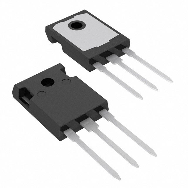
STGP40V60F IGBT Equivalent & Substitute Parts
Part Overview
The STGP40V60F is a Trench Field Stop IGBT manufactured by STMicroelectronics, rated for 600 V collector-emitter breakdown voltage with an 80 A maximum collector current and 283 W power dissipation capability. This device is packaged in a TO-220-3 through-hole configuration and is designed for high-frequency switching applications requiring robust voltage and current handling.
The STGP40V60F is classified as an obsolete product. Identification of equivalent and substitute parts is necessary to maintain design continuity, ensure supply chain availability, and support ongoing production requirements for applications utilizing this component.
Substiute Parts
Key Parameters
| Parameter | Value | Unit |
|---|---|---|
| Voltage - Collector Emitter Breakdown (Max) | 600 | V |
| Current - Collector (Ic) (Max) | 80 | A |
| Current - Collector Pulsed (Icm) | 160 | A |
| Power - Max | 283 | W |
| Vce(on) (Max) @ Vge, Ic | 2.3 V @ 15V, 40A | V |
| Gate Charge | 226 | nC |
| Switching Energy (on) | 456 | µJ |
| Switching Energy (off) | 411 | µJ |
| Td (on/off) @ 25°C | 52/208 | ns |
| Operating Temperature Range | -55 to 175 | °C (TJ) |
| Package / Case | TO-220-3 | — |
| Mounting Type | Through Hole | — |
| IGBT Type | Trench Field Stop | — |
| RoHS Status | ROHS3 Compliant | — |
Substitute Part Grouping Explanation
Substitution of the STGP40V60F is determined by electrical and mechanical compatibility within the following critical parameters:
Voltage Rating: The substitute part must operate at or above the 600 V collector-emitter breakdown voltage of the original device. The STGWA40HP65FB2 provides 650 V, which exceeds this requirement and maintains backward compatibility.
Current Rating: The substitute part must support the maximum collector current requirements of the application. The STGWA40HP65FB2 is rated for 72 A continuous collector current, which is lower than the original 80 A specification. This represents a current derating and requires application-level verification of thermal and electrical margins.
Power Dissipation: The substitute part must accommodate the thermal requirements of the application. The STGWA40HP65FB2 is rated for 227 W, which is lower than the original 283 W specification.
IGBT Type: Both devices are Trench Field Stop IGBTs, ensuring consistent switching characteristics and gate drive compatibility.
Thermal Operating Range: Both devices operate across the identical temperature range of -55°C to 175°C (TJ), ensuring thermal compatibility.
Compliance and Certifications: Both devices are ROHS3 compliant, REACH unaffected, and carry identical ECCN and HTSUS classifications, ensuring regulatory and supply chain compatibility.
Package Consideration: The substitute part uses a TO-247-3 package with long leads, whereas the original uses TO-220-3. This represents a mechanical change requiring PCB layout modification and thermal management reassessment.
Parameter Comparison
| Parameter | STGP40V60F (Original) | STGWA40HP65FB2 (Substitute) | Compatibility Notes |
|---|---|---|---|
| Manufacturer | STMicroelectronics | STMicroelectronics | Same manufacturer |
| IGBT Type | Trench Field Stop | Trench Field Stop | Identical technology |
| Voltage - Collector Emitter Breakdown (Max) | 600 V | 650 V | Substitute rated higher; backward compatible |
| Current - Collector (Ic) (Max) | 80 A | 72 A | Substitute rated lower; current derating required |
| Current - Collector Pulsed (Icm) | 160 A | 120 A | Substitute rated lower; pulsed current derating required |
| Power - Max | 283 W | 227 W | Substitute rated lower; thermal derating required |
| Vce(on) (Max) @ Vge, Ic | 2.3 V @ 15V, 40A | 2.0 V @ 15V, 40A | Substitute has lower on-state voltage |
| Gate Charge | 226 nC | 153 nC | Substitute has lower gate charge; faster switching |
| Switching Energy (off) | 411 µJ | 410 µJ | Comparable off-state switching energy |
| Td (off) @ 25°C | 208 ns | 125 ns | Substitute has faster turn-off delay |
| Operating Temperature Range | -55 to 175 °C (TJ) | -55 to 175 °C (TJ) | Identical thermal operating range |
| Package / Case | TO-220-3 | TO-247-3 | Different package; PCB layout modification required |
| Mounting Type | Through Hole | Through Hole | Both through-hole; different footprint |
| RoHS Status | ROHS3 Compliant | ROHS3 Compliant | Identical compliance |
| Product Status | Obsolete | Active | Substitute is actively manufactured |
Engineering Selection Recommendations
Product Status Consideration: The STGP40V60F is classified as obsolete, whereas the STGWA40HP65FB2 is an active product with current manufacturing support. Selection of the active substitute part ensures long-term supply chain availability and ongoing technical support from STMicroelectronics.
Compliance and Regulatory Alignment: Both devices maintain identical ROHS3 compliance, REACH unaffected status, and ECCN/HTSUS classifications. No regulatory barriers exist to substitution.
Electrical Derating: The STGWA40HP65FB2 exhibits lower maximum ratings in continuous collector current (72 A versus 80 A) and power dissipation (227 W versus 283 W). Applications operating at or near the original device's maximum ratings require thermal and electrical margin reassessment to confirm operation within the substitute part's specifications.
Voltage Margin: The substitute part's 650 V rating exceeds the original 600 V specification, providing additional voltage margin and ensuring compatibility with existing circuit voltage levels.
Switching Characteristics: The substitute part demonstrates improved switching performance, including lower gate charge (153 nC versus 226 nC) and faster turn-off delay (125 ns versus 208 ns). These characteristics may reduce switching losses and improve overall circuit efficiency, provided the gate drive circuit is compatible with the lower gate charge requirement.
Package Transition: The shift from TO-220-3 to TO-247-3 packaging requires PCB layout modification, including footprint redesign and thermal management reassessment. The TO-247 package provides improved thermal performance through enhanced lead geometry, which may offset the lower power rating in certain thermal environments.
Frequently Asked Questions (FAQ)
Q: Can the STGWA40HP65FB2 directly replace the STGP40V60F without circuit modification?
A: Direct pin-compatible replacement is not possible due to different package geometries (TO-220-3 versus TO-247-3). PCB layout modification is required. Additionally, the substitute part has lower continuous current and power ratings, requiring verification that application operating conditions remain within the substitute part's specifications.
Q: What is the impact of the lower gate charge (153 nC versus 226 nC) on gate drive circuit design?
A: Lower gate charge reduces the charge that must be supplied by the gate drive circuit during switching transitions. Existing gate drive circuits designed for the original device will operate with reduced gate current demand. No circuit modification is required, though gate drive optimization may improve switching performance.
Q: How does the lower continuous current rating (72 A versus 80 A) affect application suitability?
A: Applications operating at continuous collector currents above 72 A cannot use the substitute part without exceeding its maximum rating. Applications operating below 72 A are compatible. Thermal analysis must confirm that the application's actual operating current remains within the substitute part's specification.
Q: Are there thermal management differences between the TO-220-3 and TO-247-3 packages?
A: The TO-247-3 package provides improved thermal performance through enhanced lead geometry and larger die mounting area compared to TO-220-3. Despite the lower power rating of the substitute part, the improved package thermal characteristics may provide comparable or superior thermal performance in certain mounting configurations.
Q: Is the substitute part available in the same quantity and lead time as the original?
A: The STGWA40HP65FB2 is an active product with 1850 pieces in current inventory, whereas the STGP40V60F is obsolete. The substitute part has established supply chain availability and standard lead times from STMicroelectronics.
Q: What is the significance of the lower Vce(on) voltage (2.0 V versus 2.3 V)?
A: Lower on-state voltage reduces conduction losses during the device's conducting phase. This characteristic improves overall circuit efficiency and reduces thermal dissipation, providing a performance advantage over the original device in this parameter.
Q: Can the substitute part operate across the same temperature range as the original?
A: Yes. Both devices operate across the identical junction temperature range of -55°C to 175°C (TJ), ensuring thermal compatibility in all operating environments.
Alternative Parts

SJ6012L2TP
Littelfuse Inc.
6 Alternative Parts

JMK107BBJ476MA-RE
Taiyo Yuden
10 Alternative Parts

GMK107BBJ475MA-T
Taiyo Yuden
5 Alternative Parts
SJ6020N2ARP
Littelfuse Inc.
3 Alternative Parts
SJ6025R2ATP
Littelfuse Inc.
4 Alternative Parts

2474-05L
API Delevan Inc.
1 Alternative Parts

4590R-684K
API Delevan Inc.
1 Alternative Parts

CM6560R-334
API Delevan Inc.
1 Alternative Parts

CM6460-104
API Delevan Inc.
1 Alternative Parts

5526-12
API Delevan Inc.
1 Alternative Parts