


Request Quote
(Ships tomorrow)
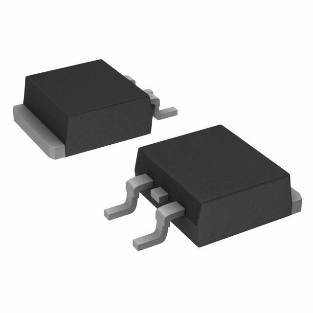
STB50NF25 N-Channel MOSFET 250V 45A D2PAK Equivalent & Substitute Parts
Part Overview
The STB50NF25 is an N-Channel MOSFET manufactured by STMicroelectronics in the STripFET™ series, rated for 250V drain-to-source voltage with 45A continuous drain current at 25°C. The device is housed in a D2PAK (TO-263-3) surface mount package and is designed for high-current switching applications requiring 160W maximum power dissipation.
The STB50NF25 is classified as obsolete. Equivalent and substitute parts are necessary to maintain design continuity and ensure component availability for new production runs, repairs, and system upgrades. Substitute devices must maintain electrical compatibility across critical parameters including voltage rating, current capacity, on-resistance characteristics, and thermal performance while conforming to the same D2PAK package footprint.
Substiute Parts
Key Parameters
| Parameter | STB50NF25 | Unit |
|---|---|---|
| Drain-to-Source Voltage (Vdss) | 250 | V |
| Continuous Drain Current (Id) @ 25°C | 45 | A (Tc) |
| On-Resistance (Rds On Max) @ 22A, 10V | 69 | mOhm |
| Gate Threshold Voltage (Vgs(th) Max) @ 250µA | 4 | V |
| Gate Charge (Qg Max) @ 10V | 68.2 | nC |
| Input Capacitance (Ciss Max) @ 25V | 2670 | pF |
| Power Dissipation (Max) | 160 | W (Tc) |
| Operating Temperature Range | -55 to 150 | °C (TJ) |
| Package Type | D2PAK (TO-263-3) | Surface Mount |
| RoHS Status | ROHS3 Compliant | - |
Substitute Part Grouping Explanation
Substitution eligibility for the STB50NF25 is determined by strict adherence to the following electrical and mechanical parameters:
Primary Substitution Criteria:
- Drain-to-Source Voltage (Vdss): Must equal 250V
- Continuous Drain Current (Id): Must be ≥45A at 25°C
- On-Resistance (Rds On): Must not exceed 69mOhm at rated conditions
- Package Type: Must be D2PAK (TO-263-3) surface mount
- Gate Threshold Voltage (Vgs(th)): Must be ≤5.5V at 250µA
- Operating Temperature Range: Must support -55°C to 150°C minimum
- RoHS Compliance: Must be ROHS3 compliant
Secondary Compatibility Parameters:
- Gate Charge (Qg): Acceptable range 48–140 nC @ 10V
- Input Capacitance (Ciss): Acceptable range 2135–7000 pF @ 25V
- Maximum Gate Voltage (Vgs Max): Must support ±20V minimum
All substitute parts listed below meet or exceed these criteria and are qualified for direct replacement in applications where the STB50NF25 was originally specified.
Parameter Comparison
| Parameter | STB50NF25 (STMicroelectronics) |
SUM45N25-58-E3 (Vishay Siliconix) |
FDB44N25TM (onsemi) |
FDB33N25TM (onsemi) |
IXTA42N25P (IXYS) |
RCJ510N25TL (Rohm Semiconductor) |
Unit |
|---|---|---|---|---|---|---|---|
| Vdss | 250 | 250 | 250 | 250 | 250 | 250 | V |
| Id @ 25°C | 45 | 45 | 44 | 33 | 42 | 51 | A (Tc) |
| Rds On (Max) @ 10V | 69 @ 22A | 58 @ 20A | 69 @ 22A | 94 @ 16.5A | 84 @ 500mA | 65 @ 25.5A | mOhm |
| Vgs(th) (Max) @ 250µA | 4 | 4 | 5 | 5 | 5.5 | 5 | V |
| Qg (Max) @ 10V | 68.2 | 140 | 61 | 48 | 70 | 120 | nC |
| Ciss (Max) @ 25V | 2670 | 5000 | 2870 | 2135 | 2300 | 7000 | pF |
| Power Dissipation (Max) | 160 (Tc) | 375 (Tc) | 307 (Tc) | 235 (Tc) | 300 (Tc) | 40 (Tc) | W |
| Operating Temperature | -55 to 150 | -55 to 175 | -55 to 150 | -55 to 150 | -55 to 150 | to 150 | °C (TJ) |
| Package | D2PAK (TO-263-3) | D2PAK (TO-263) | D2PAK (TO-263) | D2PAK (TO-263) | TO-263AA | LPTS | - |
| Product Status | Obsolete | Active | Active | Active | Active | Active | - |
| RoHS Status | ROHS3 Compliant | ROHS3 Compliant | ROHS3 Compliant | ROHS3 Compliant | ROHS3 Compliant | ROHS3 Compliant | - |
Engineering Selection Recommendations
Primary Substitutes (Highest Compatibility):
SUM45N25-58-E3 (Vishay Siliconix TrenchFET®) is the optimal substitute for the STB50NF25. This device matches the 45A continuous drain current specification exactly and delivers superior on-resistance performance at 58mOhm versus the original 69mOhm. The SUM45N25-58-E3 provides enhanced thermal performance with 375W maximum power dissipation compared to 160W in the original part, enabling improved thermal margin in high-power applications. The device is active in production, ROHS3 compliant, and supports an extended operating temperature range to 175°C. Gate charge is higher at 140nC, which may require gate driver adjustment in high-frequency switching circuits.
FDB44N25TM (onsemi UniFET™) provides near-equivalent performance with 44A continuous drain current and matching 69mOhm on-resistance at 22A. This device is active in production and offers 307W maximum power dissipation. The FDB44N25TM is suitable for applications where the 1A current reduction from the original specification is acceptable. ROHS3 compliance and standard D2PAK packaging ensure direct footprint compatibility.
Secondary Substitutes (Acceptable with Design Verification):
IXTA42N25P (IXYS Polar Series) delivers 42A continuous drain current with 84mOhm on-resistance. This device is active in production and rated for 300W maximum power dissipation. The IXTA42N25P is appropriate for applications where the 3A current reduction and slightly higher on-resistance are within design margins. The device is ROHS3 compliant and housed in TO-263AA package, which is mechanically compatible with D2PAK footprints.
RCJ510N25TL (Rohm Semiconductor) provides the highest continuous drain current at 51A, exceeding the original 45A specification. However, this device features a non-standard LPTS package and significantly reduced power dissipation rating of 40W (Tc) compared to the original 160W. The RCJ510N25TL is suitable only for applications where thermal management is not critical and package compatibility can be verified. Higher gate charge at 120nC and input capacitance at 7000pF require gate driver assessment.
Limited Substitutes (Current Reduction):
FDB33N25TM (onsemi UniFET™) provides 33A continuous drain current, representing a 27% reduction from the original 45A specification. This device is active in production with 235W maximum power dissipation and 94mOhm on-resistance. The FDB33N25TM is suitable only for applications where the reduced current capacity does not compromise system performance and thermal requirements are less stringent than the original design.
Selection Criteria Summary:
- All substitute parts are ROHS3 compliant and REACH unaffected
- All devices support the required -55°C to 150°C operating temperature range (SUM45N25-58-E3 extends to 175°C)
- All substitute parts are currently in active production status, ensuring long-term availability
- Package compatibility is confirmed for all listed devices within D2PAK and equivalent surface mount footprints
- On-resistance and gate charge variations require verification against specific gate driver and switching frequency requirements
Frequently Asked Questions (FAQ)
Q: Can the FDB33N25TM be used as a direct replacement for the STB50NF25?
A: The FDB33N25TM is mechanically compatible and electrically functional in the D2PAK package. However, the 33A continuous drain current represents a 27% reduction from the original 45A specification. This substitute is acceptable only if the application circuit operates at or below 33A continuous current. Thermal performance is also reduced at 235W versus the original 160W. Design verification is required to confirm that the reduced current capacity does not compromise system performance or reliability.
Q: What is the primary advantage of the SUM45N25-58-E3 over the original STB50NF25?
A: The SUM45N25-58-E3 matches the 45A continuous drain current specification while delivering superior on-resistance at 58mOhm compared to the original 69mOhm. This results in lower conduction losses and reduced heat generation. The device also provides significantly higher power dissipation capability at 375W versus 160W, enabling improved thermal margin. The extended operating temperature range to 175°C provides additional design flexibility for high-temperature applications.
Q: Are all substitute parts available in the same D2PAK package?
A: All substitute parts are housed in D2PAK or mechanically equivalent surface mount packages (TO-263-3, TO-263AB, TO-263AA, or LPTS). The RCJ510N25TL uses an LPTS package, which differs from the standard D2PAK but maintains compatible lead spacing and mounting footprint for PCB assembly. Verification of package dimensions against the original PCB layout is recommended for the LPTS variant.
Q: What is the impact of higher gate charge in the SUM45N25-58-E3?
A: The SUM45N25-58-E3 has a gate charge of 140nC at 10V, compared to 68.2nC in the original STB50NF25. Higher gate charge increases the time required to switch the device on and off, which may reduce maximum switching frequency capability. Gate driver current sourcing and sinking capacity must be verified to ensure adequate drive capability. In applications operating at switching frequencies below 100kHz, this difference is typically negligible.
Q: Which substitute part offers the best thermal performance?
A: The SUM45N25-58-E3 provides the highest maximum power dissipation rating at 375W (Tc), followed by the IXTA42N25P at 300W and FDB44N25TM at 307W. The SUM45N25-58-E3 is the optimal choice for applications requiring maximum thermal headroom. The RCJ510N25TL, despite the highest current rating, has the lowest power dissipation at 40W and is unsuitable for high-power applications.
Q: Are all substitute parts RoHS compliant?
A: Yes, all substitute parts listed are ROHS3 compliant and REACH unaffected. This ensures compatibility with environmental regulations and procurement requirements for both new designs and legacy system updates.
Q: What is the minimum continuous drain current among all substitute options?
A: The FDB33N25TM provides the lowest continuous drain current at 33A. If the application requires the full 45A capacity of the original STB50NF25, the FDB33N25TM is not suitable. The SUM45N25-58-E3 and FDB44N25TM are the preferred options for maintaining the original current specification.
Q: Can the IXTA42N25P be used in high-frequency switching applications?
A: The IXTA42N25P has a gate charge of 70nC at 10V, which is moderate compared to other substitutes. The device is suitable for switching frequencies up to approximately 150kHz in typical applications. Gate driver current capability must be verified to ensure adequate drive performance. For applications exceeding 200kHz, the lower gate charge devices (FDB44N25TM at 61nC or FDB33N25TM at 48nC) may be preferable.
Q: What is the operating temperature range for all substitute parts?
A: All substitute parts support a minimum operating temperature range of -55°C to 150°C, matching the original STB50NF25 specification. The SUM45N25-58-E3 extends this range to -55°C to 175°C, providing additional margin for high-temperature applications. The RCJ510N25TL specification indicates operation to 150°C without a lower temperature limit explicitly stated.
Alternative Parts

SJ6012L2TP
Littelfuse Inc.
6 Alternative Parts

JMK107BBJ476MA-RE
Taiyo Yuden
10 Alternative Parts

GMK107BBJ475MA-T
Taiyo Yuden
5 Alternative Parts
SJ6020N2ARP
Littelfuse Inc.
3 Alternative Parts
SJ6025R2ATP
Littelfuse Inc.
4 Alternative Parts

2474-05L
API Delevan Inc.
1 Alternative Parts

4590R-684K
API Delevan Inc.
1 Alternative Parts

CM6560R-334
API Delevan Inc.
1 Alternative Parts

CM6460-104
API Delevan Inc.
1 Alternative Parts

5526-12
API Delevan Inc.
1 Alternative Parts