


Request Quote
(Ships tomorrow)
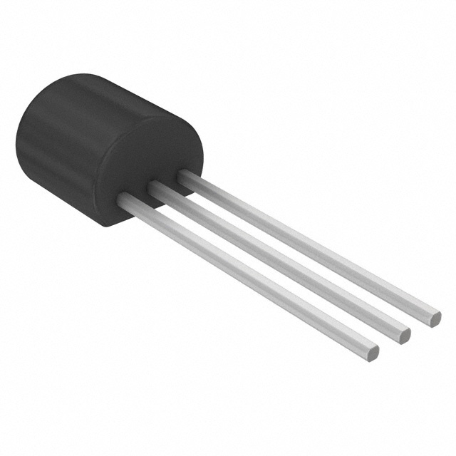
J112-D74Z JFET N-Channel Equivalent & Substitute Parts
Part Overview
The J112-D74Z is an N-Channel JFET transistor manufactured by onsemi, rated for 35 V breakdown voltage and 625 mW maximum power dissipation in a Through Hole TO-92-3 package. This device is currently in active production status. Equivalent and substitute parts are identified based on matching electrical characteristics and package compatibility to support design flexibility, inventory optimization, and supply chain continuity.
Substiute Parts
Key Parameters
| Parameter | Value | Unit |
|---|---|---|
| FET Type | N-Channel | — |
| Voltage - Breakdown (V(BR)GSS) | 35 | V |
| Current - Drain (Idss) @ Vds (Vgs=0) | 5 | mA @ 15 V |
| Voltage - Cutoff (VGS off) @ Id | 1 | V @ 1 µA |
| Resistance - RDS(On) | 50 | Ohms |
| Power - Max | 625 | mW |
| Operating Temperature | -55 to 150 | °C (TJ) |
| Mounting Type | Through Hole | — |
| Package / Case | TO-92-3 | — |
Substitute Part Grouping Explanation
Substitute parts for the J112-D74Z are qualified based on the following criteria:
- Identical FET type (N-Channel)
- Identical voltage rating (35 V breakdown)
- Identical power rating (625 mW)
- Identical package type (TO-92-3 Through Hole)
- Identical operating temperature range (-55°C to 150°C)
- Identical RoHS and REACH compliance status
The J111 and J113 meet all these requirements. Variations in drain current (Idss), cutoff voltage (VGS off), and on-resistance (RDS(On)) represent different electrical operating points within the same device family and do not preclude substitution when application requirements permit.
Parameter Comparison
| Parameter | J112-D74Z | J111 | J113 | Unit |
|---|---|---|---|---|
| Manufacturer | onsemi | onsemi | onsemi | — |
| FET Type | N-Channel | N-Channel | N-Channel | — |
| Voltage - Breakdown (V(BR)GSS) | 35 | 35 | 35 | V |
| Current - Drain (Idss) @ Vds (Vgs=0) | 5 | 20 | 2 | mA @ 15 V |
| Voltage - Cutoff (VGS off) @ Id | 1 | 3 | 0.5 | V @ 1 µA |
| Resistance - RDS(On) | 50 | 30 | 100 | Ohms |
| Power - Max | 625 | 625 | 625 | mW |
| Operating Temperature | -55 to 150 | -55 to 150 | -55 to 150 | °C (TJ) |
| Mounting Type | Through Hole | Through Hole | Through Hole | — |
| Package / Case | TO-92-3 | TO-92-3 | TO-92-3 | — |
| Product Status | Active | Active | Active | — |
| RoHS Status | ROHS3 Compliant | ROHS3 Compliant | ROHS3 Compliant | — |
| REACH Status | REACH Unaffected | REACH Unaffected | REACH Unaffected | — |
Engineering Selection Recommendations
All three devices (J112-D74Z, J111, J113) are manufactured by onsemi and maintain active production status. All are ROHS3 compliant and REACH unaffected, meeting current regulatory requirements for electronic component procurement.
Selection between these parts depends on application-specific electrical requirements:
- J111 exhibits the highest drain current (20 mA) and lowest on-resistance (30 Ohms), suitable for applications requiring lower impedance switching characteristics.
- J112-D74Z provides mid-range electrical characteristics (5 mA drain current, 50 Ohms on-resistance), representing a balanced operating point.
- J113 exhibits the lowest drain current (2 mA) and highest on-resistance (100 Ohms), suitable for applications requiring higher impedance or lower leakage current operation.
All devices share identical voltage ratings, power dissipation limits, temperature ranges, and package configurations, ensuring mechanical and thermal compatibility in circuit board designs.
Frequently Asked Questions (FAQ)
Q: Can J111 be used as a direct replacement for J112-D74Z?
A: J111 is electrically compatible within the same device family. Both share identical voltage ratings (35 V), power ratings (625 mW), package type (TO-92-3), and operating temperature range (-55°C to 150°C). However, J111 exhibits higher drain current (20 mA vs. 5 mA) and lower on-resistance (30 Ohms vs. 50 Ohms). Substitution is valid when circuit design permits these electrical variations.
Q: What is the difference between J113 and J112-D74Z?
A: J113 differs in drain current (2 mA vs. 5 mA) and on-resistance (100 Ohms vs. 50 Ohms). All other electrical and mechanical parameters are identical. J113 operates at a higher impedance point and is suitable for applications where lower leakage current is beneficial.
Q: Are all three parts available in the same packaging?
A: Yes. J112-D74Z, J111, and J113 are all supplied in TO-92-3 Through Hole packages with formed leads. They are mechanically interchangeable on printed circuit boards designed for TO-92-3 components.
Q: Do these parts meet current compliance standards?
A: All three devices are ROHS3 compliant and REACH unaffected, meeting current regulatory requirements for electronic component use in regulated markets.
Q: What determines whether a substitute part is acceptable for my application?
A: Substitution validity depends on whether the application circuit can tolerate the electrical parameter variations shown in the Parameter Comparison table. Drain current (Idss), cutoff voltage (VGS off), and on-resistance (RDS(On)) differences must be evaluated against specific circuit requirements for gain, switching speed, and impedance characteristics.
Alternative Parts

SJ6012L2TP
Littelfuse Inc.
6 Alternative Parts

JMK107BBJ476MA-RE
Taiyo Yuden
10 Alternative Parts

GMK107BBJ475MA-T
Taiyo Yuden
5 Alternative Parts
SJ6020N2ARP
Littelfuse Inc.
3 Alternative Parts
SJ6025R2ATP
Littelfuse Inc.
4 Alternative Parts

2474-05L
API Delevan Inc.
1 Alternative Parts

4590R-684K
API Delevan Inc.
1 Alternative Parts

CM6560R-334
API Delevan Inc.
1 Alternative Parts

CM6460-104
API Delevan Inc.
1 Alternative Parts

5526-12
API Delevan Inc.
1 Alternative Parts