


Request Quote
(Ships tomorrow)
FDMS8880 N-Channel 30V MOSFET Equivalent & Substitute Parts
Part Overview
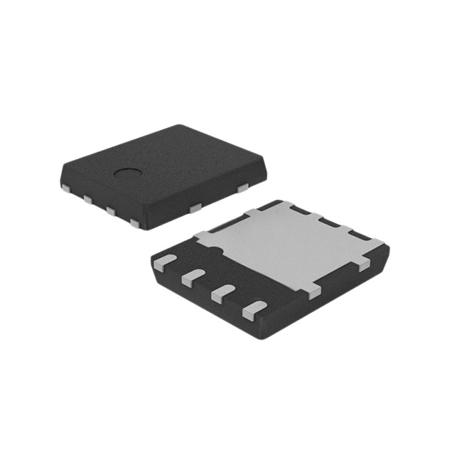
The FDMS8880 is an N-Channel 30V MOSFET manufactured by onsemi in the PowerTrench® series, housed in an 8-PQFN (5x6) surface mount package. This device is rated for 13.5A continuous drain current (Ta) and 21A (Tc) with a maximum Rds(on) of 8.5mOhm at 10V gate-source voltage. The FDMS8880 is classified as obsolete, necessitating identification of functionally equivalent alternatives for new designs and ongoing production support. Substitute parts must maintain compatibility across drain-source voltage ratings, continuous drain current specifications, gate charge characteristics, and surface mount packaging requirements.
Substiute Parts
Key Parameters
| Parameter | FDMS8880 Value | Unit |
|---|---|---|
| Drain to Source Voltage (Vdss) | 30 | V |
| Current - Continuous Drain (Id) @ 25°C (Ta) | 13.5 | A |
| Current - Continuous Drain (Id) @ 25°C (Tc) | 21 | A |
| Rds(on) Max @ Id, Vgs | 8.5 mOhm @ 13.5A, 10V | mOhm |
| Gate Charge (Qg) Max @ Vgs | 33 | nC @ 10V |
| Input Capacitance (Ciss) Max @ Vds | 1585 | pF @ 15V |
| Vgs(th) Max @ Id | 2.5 | V @ 250µA |
| Vgs Max | ±20 | V |
| Power Dissipation Max (Ta) | 2.5 | W |
| Power Dissipation Max (Tc) | 42 | W |
| Operating Temperature Range | -55 to 150 | °C (TJ) |
| Mounting Type | Surface Mount | - |
| Package / Case | 8-PowerTDFN | - |
| RoHS Status | ROHS3 Compliant | - |
| Moisture Sensitivity Level (MSL) | 1 (Unlimited) | - |
Substitute Part Grouping Explanation
Substitute parts for the FDMS8880 are selected based on strict electrical and mechanical compatibility criteria. All substitute devices must meet the following requirements:
Critical Matching Parameters:
- Drain to Source Voltage (Vdss): 30V minimum
- Continuous Drain Current (Id) @ 25°C: Minimum 13.5A (Ta) or equivalent thermal performance
- Gate-Source Voltage (Vgs) Range: ±20V or greater
- Operating Temperature Range: -55°C to 150°C (TJ)
- Surface Mount Packaging: 8-pin configurations with 5x6mm footprint compatibility
- RoHS3 Compliance and MSL Level 1 rating
Substitution Logic: Devices are grouped as direct substitutes when they maintain Vdss at 30V, support continuous drain current at or above 13.5A (Ta), and provide equivalent or superior Rds(on) performance. Gate charge (Qg) and input capacitance (Ciss) variations are acceptable within the scope of circuit design margins. Package variants (8-PQFN, 8-DFN, 8-VSON, PG-TDSON-8-5) are considered compatible when physical footprints align with 5x6mm surface mount requirements.
Parameter Comparison
| Parameter | FDMS8880 | AON6414AL | BSC080N03LSGATMA1 | BSC080N03MSGATMA1 | BSC090N03LSGATMA1 | BSC100N03MSGATMA1 | BSC120N03LSGATMA1 | BSC120N03MSGATMA1 | CSD17307Q5A | CSD17507Q5A | CSD17527Q5A |
|---|---|---|---|---|---|---|---|---|---|---|---|
| Manufacturer | onsemi | Alpha & Omega Semiconductor Inc. | Infineon Technologies | Infineon Technologies | Infineon Technologies | Infineon Technologies | Infineon Technologies | Infineon Technologies | Texas Instruments | Texas Instruments | Texas Instruments |
| Vdss (V) | 30 | 30 | 30 | 30 | 30 | 30 | 30 | 30 | 30 | 30 | 30 |
| Id @ 25°C (Ta) (A) | 13.5 | 13 | 14 | 13 | 13 | 12 | 12 | 11 | 14 | 13 | — |
| Id @ 25°C (Tc) (A) | 21 | 30 | 53 | 53 | 48 | 44 | 39 | 39 | 73 | 65 | 65 |
| Rds(on) Max (mOhm) | 8.5 @ 13.5A, 10V | 8 @ 20A, 10V | 8 @ 30A, 10V | 8 @ 30A, 10V | 9 @ 30A, 10V | 10 @ 30A, 10V | 12 @ 30A, 10V | 12 @ 30A, 10V | 10.5 @ 11A, 8V | 10.8 @ 11A, 10V | 10.8 @ 11A, 10V |
| Qg Max (nC) | 33 @ 10V | 24 @ 10V | 21 @ 10V | 27 @ 10V | 18 @ 10V | 23 @ 10V | 15 @ 10V | 20 @ 10V | 5.2 @ 4.5V | 3.6 @ 4.5V | 3.4 @ 4.5V |
| Ciss Max (pF) | 1585 @ 15V | 1380 @ 15V | 1700 @ 15V | 2100 @ 15V | 1500 @ 15V | 1700 @ 15V | 1200 @ 15V | 1500 @ 15V | 700 @ 15V | 530 @ 15V | 506 @ 15V |
| Vgs(th) Max (V) | 2.5 @ 250µA | 2.5 @ 250µA | 2.2 @ 250µA | 2 @ 250µA | 2.2 @ 250µA | 2 @ 250µA | 2.2 @ 250µA | 2 @ 250µA | 1.8 @ 250µA | 2.1 @ 250µA | 2 @ 250µA |
| Vgs Max (V) | ±20 | ±20 | ±20 | ±20 | ±20 | ±20 | ±20 | ±20 | +10, -8 | ±20 | ±20 |
| Power Dissipation (Ta) (W) | 2.5 | 2.3 | 2.5 | 2.5 | 2.5 | 2.5 | 2.5 | 2.5 | 3 | 3 | 3 |
| Power Dissipation (Tc) (W) | 42 | 31 | 35 | 35 | 32 | 30 | 28 | 28 | — | — | — |
| Operating Temperature (°C) | -55 to 150 | -55 to 150 | -55 to 150 | -55 to 150 | -55 to 150 | -55 to 150 | -55 to 150 | -55 to 150 | -55 to 150 | -55 to 150 | -55 to 150 |
| Package | 8-PowerTDFN (8-PQFN) | 8-VDFN Exposed Pad | PG-TDSON-8-5 | PG-TDSON-8-5 | PG-TDSON-8-5 | PG-TDSON-8-5 | PG-TDSON-8-5 | PG-TDSON-8-5 | 8-VSONP (5x6) | 8-VSONP (5x6) | 8-VSONP (5x6) |
| Product Status | Obsolete | Active | Obsolete | Not For New Designs | Active | Not For New Designs | Active | Active | Active | Active | Active |
| RoHS Status | ROHS3 Compliant | ROHS3 Compliant | ROHS3 Compliant | ROHS3 Compliant | ROHS3 Compliant | ROHS3 Compliant | ROHS3 Compliant | ROHS3 Compliant | ROHS3 Compliant | ROHS3 Compliant | ROHS3 Compliant |
| MSL Rating | 1 (Unlimited) | 1 (Unlimited) | 1 (Unlimited) | 1 (Unlimited) | 1 (Unlimited) | 1 (Unlimited) | 1 (Unlimited) | 1 (Unlimited) | 1 (Unlimited) | 1 (Unlimited) | 1 (Unlimited) |
Engineering Selection Recommendations
Primary Substitutes (Active Product Status):
The following devices are recommended as primary substitutes for the FDMS8880 due to active product status and full compliance with RoHS3 and MSL Level 1 requirements:
AON6414AL (Alpha & Omega Semiconductor Inc.) – Active status. Provides 13A (Ta) and 30A (Tc) continuous drain current with 8mOhm Rds(on) at 20A, 10V. Gate charge of 24nC is lower than the FDMS8880, reducing switching losses. Input capacitance of 1380pF is within acceptable range. 8-DFN (5x6) package maintains footprint compatibility.
BSC090N03LSGATMA1 (Infineon Technologies OptiMOS™) – Active status. Rated for 13A (Ta) and 48A (Tc) with 9mOhm Rds(on) at 30A, 10V. Gate charge of 18nC provides improved switching performance. Vgs(th) of 2.2V and input capacitance of 1500pF are compatible with existing circuit designs. PG-TDSON-8-5 package maintains 5x6mm footprint.
BSC120N03LSGATMA1 (Infineon Technologies OptiMOS™) – Active status. Rated for 12A (Ta) and 39A (Tc) with 12mOhm Rds(on) at 30A, 10V. Gate charge of 15nC offers superior switching characteristics. Input capacitance of 1200pF is lower than the FDMS8880. Suitable for applications where gate charge minimization is beneficial.
CSD17307Q5A (Texas Instruments NexFET™) – Active status. Provides 14A (Ta) and 73A (Tc) with 10.5mOhm Rds(on) at 11A, 8V. Significantly lower gate charge of 5.2nC and input capacitance of 700pF enable high-frequency switching applications. Vgs range of +10V, -8V requires circuit verification. 8-VSONP (5x6) package maintains footprint compatibility.
CSD17507Q5A (Texas Instruments NexFET™) – Active status. Rated for 13A (Ta) and 65A (Tc) with 10.8mOhm Rds(on) at 11A, 10V. Gate charge of 3.6nC and input capacitance of 530pF provide excellent high-frequency performance. Vgs range of ±20V matches the FDMS8880. 8-VSONP (5x6) package maintains footprint compatibility.
CSD17527Q5A (Texas Instruments NexFET™) – Active status. Rated for 65A (Tc) with 10.8mOhm Rds(on) at 11A, 10V. Gate charge of 3.4nC and input capacitance of 506pF are optimal for switching applications. Vgs range of ±20V matches the FDMS8880. 8-VSONP (5x6) package maintains footprint compatibility.
Secondary Substitutes (Not For New Designs / Obsolete Status):
BSC080N03LSGATMA1 (Infineon Technologies OptiMOS™) – Obsolete status. Rated for 14A (Ta) and 53A (Tc) with 8mOhm Rds(on) at 30A, 10V. Gate charge of 21nC and input capacitance of 1700pF are acceptable. Suitable for legacy production support only.
BSC080N03MSGATMA1 (Infineon Technologies OptiMOS™) – Not For New Designs status. Rated for 13A (Ta) and 53A (Tc) with 8mOhm Rds(on) at 30A, 10V. Gate charge of 27nC and input capacitance of 2100pF are higher than preferred. Suitable for legacy production support only.
BSC100N03MSGATMA1 (Infineon Technologies OptiMOS™) – Not For New Designs status. Rated for 12A (Ta) and 44A (Tc) with 10mOhm Rds(on) at 30A, 10V. Gate charge of 23nC and input capacitance of 1700pF are acceptable. Suitable for legacy production support only.
BSC120N03MSGATMA1 (Infineon Technologies OptiMOS™) – Active status. Rated for 11A (Ta) and 39A (Tc) with 12mOhm Rds(on) at 30A, 10V. Gate charge of 20nC and input capacitance of 1500pF are acceptable. Suitable for applications with lower continuous current requirements.
Frequently Asked Questions (FAQ)
Q: Can the FDMS8880 be directly replaced with any of the listed substitutes without circuit modification?
A: Direct replacement is possible for devices maintaining the same Vdss (30V), continuous drain current (≥13.5A Ta), and Vgs range (±20V). AON6414AL, BSC090N03LSGATMA1, BSC120N03LSGATMA1, CSD17507Q5A, and CSD17527Q5A are direct replacements. Devices with different Vgs ranges (CSD17307Q5A: +10V, -8V) require circuit verification. Gate charge and input capacitance variations may affect switching frequency and EMI characteristics but do not prevent functional replacement.
Q: What is the significance of gate charge (Qg) differences between the FDMS8880 and substitute parts?
A: Gate charge determines the energy required to switch the MOSFET on and off. The FDMS8880 has a gate charge of 33nC at 10V. Substitutes with lower gate charge (CSD17507Q5A: 3.6nC, CSD17527Q5A: 3.4nC) reduce switching losses and enable higher switching frequencies. Substitutes with higher gate charge (BSC080N03MSGATMA1: 27nC) increase switching losses. Selection depends on circuit switching frequency and thermal management requirements.
Q: Are all substitute parts compatible with the 8-PowerTDFN package footprint?
A: The FDMS8880 uses an 8-PowerTDFN (8-PQFN 5x6) package. Substitute packages include 8-DFN (5x6), PG-TDSON-8-5, and 8-VSONP (5x6). All maintain 5x6mm footprints and 8-pin configurations, ensuring PCB layout compatibility. Pin assignments must be verified against individual datasheets to confirm functional equivalence.
Q: Which substitute parts are recommended for new designs?
A: For new designs, select from devices with Active product status: AON6414AL, BSC090N03LSGATMA1, BSC120N03LSGATMA1, BSC120N03MSGATMA1, CSD17307Q5A, CSD17507Q5A, and CSD17527Q5A. These devices have full manufacturer support and long-term availability. Avoid devices marked as Obsolete or Not For New Designs for new product development.
Q: What is the impact of Rds(on) variations on circuit performance?
A: Rds(on) determines conduction losses and heat dissipation. The FDMS8880 has 8.5mOhm Rds(on) at 13.5A, 10V. Substitutes range from 8mOhm (AON6414AL, BSC080N03LSGATMA1, BSC080N03MSGATMA1) to 12mOhm (BSC120N03LSGATMA1, BSC120N03MSGATMA1). Lower Rds(on) values reduce power dissipation and heat generation. Higher values increase thermal load. Selection depends on circuit current levels and thermal design margins.
Q: Are all substitute parts RoHS3 compliant and MSL Level 1 rated?
A: Yes. All listed substitute parts are RoHS3 compliant and carry MSL Level 1 (Unlimited) moisture sensitivity ratings, matching the FDMS8880 compliance profile. This ensures compatibility with standard manufacturing processes and long-term storage without special handling requirements.
Q: How do input capacitance (Ciss) differences affect circuit design?
A: Input capacitance affects gate drive circuit design and switching speed. The FDMS8880 has 1585pF Ciss at 15V. Substitutes range from 506pF (CSD17527Q5A) to 2100pF (BSC080N03MSGATMA1). Lower capacitance values reduce gate drive current requirements and enable faster switching. Higher values increase gate drive demands. Circuit gate drive capability must accommodate the selected device's Ciss value.
Q: What is the difference between Ta and Tc current ratings?
A: Ta (ambient temperature) and Tc (case temperature) represent continuous drain current under different thermal conditions. Ta assumes ambient air cooling, while Tc assumes direct case cooling or thermal management. The FDMS8880 is rated for 13.5A (Ta) and 21A (Tc). Substitutes provide higher Tc ratings (up to 73A for CSD17307Q5A), indicating superior thermal performance under active cooling. Selection depends on actual thermal management implementation.
Q: Can substitutes with lower Vgs(th) values be used interchangeably?
A: Vgs(th) (gate-source threshold voltage) determines the gate voltage required to turn the MOSFET on. The FDMS8880 has 2.5V Vgs(th). Substitutes range from 1.8V (CSD17307Q5A) to 2.5V (AON6414AL). Lower threshold voltages enable operation with lower gate drive voltages but may increase susceptibility to noise-induced false switching. Circuit gate drive voltage must exceed the selected device's Vgs(th) by adequate margin for reliable operation.
Q: What packaging considerations apply when substituting the FDMS8880?
A: The FDMS8880 uses 8-PowerTDFN (8-PQFN 5x6) packaging. All substitute parts use 8-pin surface mount packages with 5x6mm footprints (8-DFN, PG-TDSON-8-5, 8-VSONP). Pin assignments and thermal pad configurations may differ. PCB layout, thermal via placement, and solder reflow profiles must be verified against the specific substitute device datasheet to ensure proper thermal performance and electrical connectivity.
Alternative Parts

SJ6012L2TP
Littelfuse Inc.
6 Alternative Parts

JMK107BBJ476MA-RE
Taiyo Yuden
10 Alternative Parts

GMK107BBJ475MA-T
Taiyo Yuden
5 Alternative Parts
SJ6020N2ARP
Littelfuse Inc.
3 Alternative Parts
SJ6025R2ATP
Littelfuse Inc.
4 Alternative Parts

2474-05L
API Delevan Inc.
1 Alternative Parts

4590R-684K
API Delevan Inc.
1 Alternative Parts

CM6560R-334
API Delevan Inc.
1 Alternative Parts

CM6460-104
API Delevan Inc.
1 Alternative Parts

5526-12
API Delevan Inc.
1 Alternative Parts