


Request Quote
(Ships tomorrow)
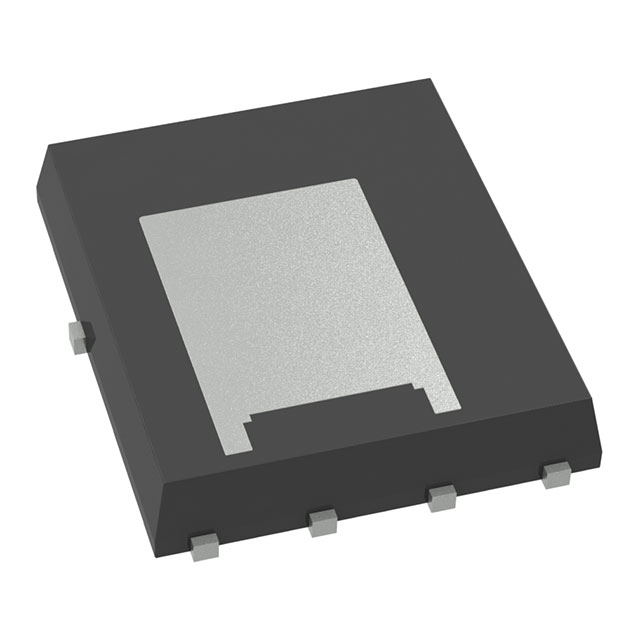
FDMS2508SDC N-Channel MOSFET Equivalent & Substitute Parts
Part Overview
The FDMS2508SDC is an N-Channel MOSFET manufactured by onsemi, rated for 25V drain-to-source voltage with continuous drain current of 34A (Ta) and 49A (Tc). This device features the Dual Cool™, PowerTrench®, and SyncFET™ technology series and is packaged in an 8-PQFN (5x6) surface mount configuration. The FDMS2508SDC is classified as obsolete, making equivalent and substitute parts necessary for new designs and ongoing production requirements.
Substiute Parts
Key Parameters
| Parameter | Value | Unit |
|---|---|---|
| Drain-to-Source Voltage (Vdss) | 25 | V |
| Continuous Drain Current @ 25°C (Ta) | 34 | A |
| Continuous Drain Current @ 25°C (Tc) | 49 | A |
| On-Resistance (Rds On) @ 28A, 10V | 1.95 | mOhm |
| Gate Threshold Voltage (Vgs(th)) @ 1mA | 3 | V |
| Gate Charge (Qg) @ 10V | 69 | nC |
| Input Capacitance (Ciss) @ 13V | 4515 | pF |
| Power Dissipation (Ta) | 3.3 | W |
| Power Dissipation (Tc) | 78 | W |
| Operating Temperature Range | -55 to 150 | °C |
| Mounting Type | Surface Mount | — |
| Package | 8-PowerTDFN (5x6) | — |
Substitute Part Grouping Explanation
Substitution of the FDMS2508SDC is determined by the following critical electrical and mechanical parameters:
Primary Substitution Criteria:
- Drain-to-Source Voltage (Vdss): Must be equal to or greater than 25V
- Continuous Drain Current (Id): Must meet or exceed 34A at Ta (25°C ambient)
- On-Resistance (Rds On): Lower or equivalent values ensure compatible switching performance
- Gate Threshold Voltage (Vgs(th)): Must be compatible with existing gate drive circuitry
- Operating Temperature Range: Must span -55°C to 150°C
- Mounting Type: Surface mount configuration required
- Package Form Factor: 8-pin power package in 5x6mm footprint
Secondary Compatibility Factors:
- Gate Charge (Qg) and Input Capacitance (Ciss) affect switching speed and gate drive requirements
- Power Dissipation ratings determine thermal management capability
- Moisture Sensitivity Level (MSL) and compliance certifications (RoHS, REACH) ensure manufacturing and environmental compatibility
The substitute parts listed below satisfy the primary electrical requirements while maintaining surface mount compatibility. Variations in secondary parameters reflect different technology nodes and manufacturer implementations.
Parameter Comparison
| Parameter | FDMS2508SDC (onsemi) | BSC024NE2LSATMA1 (Infineon) | CSD16325Q5 (TI) | CSD16414Q5 (TI) | CSD17576Q5B (TI) | CSD17576Q5BT (TI) | RJK0346DPA-01#J0B (Renesas) |
|---|---|---|---|---|---|---|---|
| Vdss (V) | 25 | 25 | 25 | 25 | 30 | 30 | 30 |
| Id @ Ta (A) | 34 | 25 | 33 | 34 | 100 | 100 | 65 |
| Id @ Tc (A) | 49 | 110 | 100 | 100 | 100 | 100 | — |
| Rds On (mOhm) | 1.95 @ 28A, 10V | 2.4 @ 30A, 10V | 2.0 @ 30A, 8V | 1.9 @ 30A, 10V | 2.0 @ 25A, 10V | 2.0 @ 25A, 10V | 1.8 @ 25A, 10V |
| Vgs(th) (V) | 3 @ 1mA | 2 @ 250µA | 1.4 @ 250µA | 2 @ 250µA | 1.8 @ 250µA | 1.8 @ 250µA | — |
| Qg (nC) | 69 @ 10V | 23 @ 10V | 25 @ 4.5V | 21 @ 4.5V | 68 @ 10V | 32 @ 4.5V | 49 @ 10V |
| Ciss (pF) | 4515 @ 13V | 1700 @ 12V | 4000 @ 12.5V | 3650 @ 12.5V | 4430 @ 15V | 4430 @ 15V | 7650 @ 10V |
| Power Dissipation Ta (W) | 3.3 | 2.5 | 3.1 | 3.2 | 3.1 | 3.1 | — |
| Power Dissipation Tc (W) | 78 | 48 | — | — | 125 | 125 | 65 |
| Operating Temperature (°C) | -55 to 150 | -55 to 150 | -55 to 150 | -55 to 150 | -55 to 150 | -55 to 150 | — |
| Package | 8-PowerTDFN (5x6) | PG-TDSON-8-5 | 8-VSON-CLIP (5x6) | 8-VSON-CLIP (5x6) | 8-VSONP (5x6) | 8-VSONP (5x6) | 8-WPAK |
| Product Status | Obsolete | Active | Active | Active | Active | Active | Active |
Engineering Selection Recommendations
Primary Substitutes (25V Vdss, 34A+ Id @ Ta):
The CSD16414Q5 from Texas Instruments provides the closest electrical match to the FDMS2508SDC. It maintains 25V Vdss, 34A continuous drain current at Ta, and 1.9mOhm on-resistance at 10V gate drive. The CSD16414Q5 is active in production status with RoHS3 compliance and REACH unaffected certification. The 8-VSON-CLIP (5x6) package is mechanically compatible with the original 8-PowerTDFN footprint.
The CSD16325Q5 from Texas Instruments offers 25V Vdss with 33A continuous drain current at Ta and 2.0mOhm on-resistance. This device is active in production with equivalent thermal and compliance characteristics. The slightly lower gate threshold voltage (1.4V) may require gate drive circuit evaluation in applications with marginal drive voltage margins.
The BSC024NE2LSATMA1 from Infineon Technologies provides 25V Vdss with 25A continuous drain current at Ta. While the ambient temperature current rating is lower than the original part, the 110A Tc rating and 2.4mOhm on-resistance support applications with adequate thermal management. This device is active in production with RoHS3 compliance and high inventory availability.
Secondary Substitutes (30V Vdss, Higher Current Capability):
The CSD17576Q5B and CSD17576Q5BT from Texas Instruments are rated for 30V Vdss with 100A continuous drain current at Ta. These devices provide enhanced voltage and current headroom for applications requiring higher performance margins. Both variants are active in production with RoHS3 compliance. The CSD17576Q5BT is packaged in Tape & Reel format, while CSD17576Q5B is available in Cut Tape and Digi-Reel® packaging.
The RJK0346DPA-01#J0B from Renesas Electronics Corporation is rated for 30V Vdss with 65A continuous drain current at Ta and 1.8mOhm on-resistance. This device is active in production with RoHS3 compliance. The 8-WPAK package differs from the original footprint and requires PCB layout verification.
Compliance and Production Status:
All recommended substitute parts are active in production status, ensuring long-term availability and supply chain stability. All devices maintain the required operating temperature range of -55°C to 150°C. Moisture Sensitivity Level 1 (Unlimited) is maintained across all substitutes, supporting standard manufacturing processes. REACH unaffected and EAR99 ECCN classifications are consistent across all parts.
Frequently Asked Questions (FAQ)
Q: Can the CSD16414Q5 directly replace the FDMS2508SDC without PCB modifications?
A: The CSD16414Q5 maintains the same 8-pin power package footprint (5x6mm) as the FDMS2508SDC. Pin-to-pin compatibility exists between the 8-VSON-CLIP and 8-PowerTDFN packages. No PCB layout modifications are required for direct substitution. Gate drive voltage compatibility should be verified, as the CSD16414Q5 supports ±16V to -12V Vgs maximum compared to the original ±20V specification.
Q: What is the impact of lower gate threshold voltage in the CSD16325Q5?
A: The CSD16325Q5 has a gate threshold voltage of 1.4V compared to the FDMS2508SDC at 3V. This lower threshold voltage reduces the minimum gate drive voltage required for device turn-on. In applications with marginal gate drive voltage (near 3V), the CSD16325Q5 may exhibit unintended partial conduction. Gate drive circuits designed for 10V or higher operation are unaffected by this parameter difference.
Q: Why does the BSC024NE2LSATMA1 have lower Ta current rating but higher Tc rating?
A: The BSC024NE2LSATMA1 achieves 110A Tc rating through superior thermal design and lower junction-to-case thermal resistance. The 25A Ta rating reflects the device's performance under ambient temperature conditions without active cooling. Applications with adequate heat sinking can utilize the higher Tc current capability. Thermal management design must be evaluated for each application.
Q: Are the CSD17576Q5B and CSD17576Q5BT electrically identical?
A: The CSD17576Q5B and CSD17576Q5BT are electrically identical N-Channel MOSFETs rated for 30V Vdss and 100A Ta current. The primary difference is packaging format: CSD17576Q5B is supplied in Cut Tape and Digi-Reel® format, while CSD17576Q5BT is supplied in Tape & Reel format. Both devices maintain identical electrical specifications and compliance certifications.
Q: What is the significance of the 30V Vdss rating in the CSD17576 and RJK0346 devices?
A: The 30V Vdss rating provides 5V additional voltage margin above the 25V specification of the FDMS2508SDC. This higher rating allows operation in circuits with transient voltage spikes or design margin requirements. The 30V devices are suitable for applications where the original 25V specification is marginal. Circuit voltage stress analysis must confirm that 25V Vdss is sufficient for the intended application before selecting lower-voltage alternatives.
Q: How do gate charge differences affect switching frequency performance?
A: Gate charge (Qg) directly impacts gate drive power dissipation and switching speed. The FDMS2508SDC requires 69nC at 10V gate drive. The CSD16325Q5 requires only 25nC at 4.5V, reducing gate drive losses. The CSD17576Q5B requires 68nC at 10V, matching the original specification. Higher gate charge devices require proportionally higher gate drive current to achieve equivalent switching speeds. Gate drive circuit design must accommodate the selected device's gate charge specification.
Q: Is the RJK0346DPA-01#J0B package compatible with the original PCB layout?
A: The RJK0346DPA-01#J0B uses an 8-WPAK package, which differs from the original 8-PowerTDFN footprint. The 8-WPAK package has different pin spacing and thermal pad dimensions. PCB layout modifications are required for this substitution. Pin assignment verification and thermal pad redesign are necessary before implementation.
Q: What compliance certifications are maintained across all substitute parts?
A: All substitute parts maintain REACH unaffected status and EAR99 ECCN classification, matching the original FDMS2508SDC. The CSD16414Q5, CSD17576Q5B, CSD17576Q5BT, BSC024NE2LSATMA1, and RJK0346DPA-01#J0B all carry RoHS3 compliance certification. Moisture Sensitivity Level 1 (Unlimited) is maintained across all devices, supporting standard manufacturing processes without special handling requirements.
Q: Can multiple substitute parts be used interchangeably in production?
A: The CSD16414Q5 and CSD16325Q5 are mechanically and electrically compatible for direct substitution within the same PCB design. The CSD17576Q5B and CSD17576Q5BT are interchangeable with each other. However, switching between the 25V device group (CSD16414Q5, CSD16325Q5, BSC024NE2LSATMA1) and the 30V device group (CSD17576Q5B, CSD17576Q5BT) requires circuit voltage stress analysis. The RJK0346DPA-01#J0B requires separate PCB layout due to package differences. Production qualification testing is required before implementing any substitution.
Alternative Parts

SJ6012L2TP
Littelfuse Inc.
6 Alternative Parts

JMK107BBJ476MA-RE
Taiyo Yuden
10 Alternative Parts

GMK107BBJ475MA-T
Taiyo Yuden
5 Alternative Parts
SJ6020N2ARP
Littelfuse Inc.
3 Alternative Parts
SJ6025R2ATP
Littelfuse Inc.
4 Alternative Parts

2474-05L
API Delevan Inc.
1 Alternative Parts

4590R-684K
API Delevan Inc.
1 Alternative Parts

CM6560R-334
API Delevan Inc.
1 Alternative Parts

CM6460-104
API Delevan Inc.
1 Alternative Parts

5526-12
API Delevan Inc.
1 Alternative Parts