


Request Quote
(Ships tomorrow)
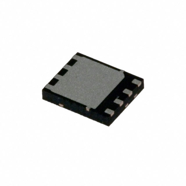
FDMC8854 N-Channel 30V 15A MOSFET Equivalent & Substitute Parts
Part Overview
The FDMC8854 is an N-Channel 30V 15A MOSFET manufactured by onsemi in the PowerTrench® series, housed in an 8-MLP (3.3x3.3) surface mount package. This device is classified as obsolete, necessitating identification of active equivalent and substitute components for new designs and production continuity. The part operates across a temperature range of -55°C to 150°C (TJ) and is RoHS3 compliant with MSL 1 (Unlimited) moisture sensitivity rating.
Substiute Parts
Key Parameters
| Parameter | Value | Unit |
|---|---|---|
| Drain to Source Voltage (Vdss) | 30 | V |
| Continuous Drain Current (Id) @ 25°C | 15 | A (Tc) |
| Rds On (Max) @ Id, Vgs | 5.7 | mOhm @ 15A, 10V |
| Gate Threshold Voltage (Vgs(th)) @ Id | 3 | V @ 250µA |
| Gate Charge (Qg) @ Vgs | 57 | nC @ 10V |
| Input Capacitance (Ciss) @ Vds | 3405 | pF @ 10V |
| Power Dissipation (Max) | 2 / 41 | W (Ta) / W (Tc) |
| Operating Temperature Range | -55 to 150 | °C (TJ) |
| Mounting Type | Surface Mount | - |
| Package | 8-PowerWDFN (3.3x3.3) | - |
| FET Type | N-Channel | - |
| Technology | MOSFET (Metal Oxide) | - |
Substitute Part Grouping Explanation
Substitution of the FDMC8854 is determined by the following critical parameters:
Electrical Compatibility Requirements:
- Drain to Source Voltage (Vdss) must be ≥30V
- Continuous Drain Current (Id) must be ≥15A at 25°C
- Rds On (Max) performance at specified gate voltage and current
- Gate Threshold Voltage (Vgs(th)) within acceptable operating range
- Gate Charge (Qg) and Input Capacitance (Ciss) for switching characteristics
- Operating temperature range: -55°C to 150°C (TJ)
Mechanical Compatibility Requirements:
- Surface mount technology
- 8-pin package configuration
- Physical dimensions compatible with 3.3x3.3mm footprint area
Compliance Requirements:
- RoHS3 compliance
- MSL 1 (Unlimited) moisture sensitivity
- REACH unaffected status
- EAR99 export classification
Substitute parts listed below meet or exceed these parameters while maintaining functional equivalence for the FDMC8854 in typical application circuits.
Parameter Comparison
| Parameter | FDMC8854 | BSZ050N03LSGATMA1 | BSZ050N03MSGATMA1 | CSD16406Q3 | CSD17552Q3A | CSD17578Q3A | CSD17578Q3AT | RQ3E130BNTB | STL11N3LLH6 |
|---|---|---|---|---|---|---|---|---|---|
| Manufacturer | onsemi | Infineon | Infineon | Texas Instruments | Texas Instruments | Texas Instruments | Texas Instruments | Rohm | STMicroelectronics |
| Vdss (V) | 30 | 30 | 30 | 25 | 30 | 30 | 30 | 30 | 30 |
| Id @ 25°C (A) | 15 (Tc) | 16 (Ta) / 40 (Tc) | 15 (Ta) / 40 (Tc) | 19 (Ta) / 60 (Tc) | 15 (Ta) / 60 (Tc) | 20 (Ta) | 20 (Ta) | 13 (Ta) | 11 (Tc) |
| Rds On (Max) (mOhm) | 5.7 @ 15A, 10V | 5 @ 20A, 10V | 4.5 @ 20A, 10V | 5.3 @ 20A, 10V | 6 @ 11A, 10V | 7.3 @ 10A, 10V | 7.3 @ 10A, 10V | 6 @ 13A, 10V | 7.5 @ 5.5A, 10V |
| Vgs(th) (V) | 3 @ 250µA | 2.2 @ 250µA | 2 @ 250µA | 2.2 @ 250µA | 1.9 @ 250µA | 1.9 @ 250µA | 1.9 @ 250µA | 2.5 @ 1mA | 1 @ 250µA (Min) |
| Qg (nC) | 57 @ 10V | 35 @ 10V | 46 @ 10V | 8.1 @ 4.5V | 12 @ 4.5V | 22.2 @ 10V | 22.2 @ 10V | 36 @ 10V | 17 @ 4.5V |
| Ciss (pF) | 3405 @ 10V | 2800 @ 15V | 3600 @ 15V | 1100 @ 12.5V | 2050 @ 15V | 1590 @ 15V | 1590 @ 15V | 1900 @ 15V | 1690 @ 24V |
| Power Dissipation (W) | 2 (Ta) / 41 (Tc) | 2.1 (Ta) / 50 (Tc) | 2.1 (Ta) / 48 (Tc) | 2.7 (Ta) | 2.6 (Ta) | 3.2 (Ta) / 37 (Tc) | 3.2 (Ta) / 37 (Tc) | 2 (Ta) | 2 (Ta) / 50 (Tc) |
| Operating Temp (°C) | -55 to 150 | -55 to 150 | -55 to 150 | -55 to 150 | -55 to 150 | -55 to 150 | -55 to 150 | -55 to 150 | -55 to 150 |
| Package Type | 8-PowerWDFN | 8-PowerTDFN | 8-PowerTDFN | 8-PowerTDFN | 8-PowerVDFN | 8-PowerVDFN | 8-PowerVDFN | 8-PowerVDFN | 8-PowerVDFN |
| Product Status | Obsolete | Active | Active | Active | Active | Active | Active | Active | Active |
| RoHS3 Compliant | Yes | Yes | Yes | Yes | Yes | Yes | Yes | Yes | Yes |
| MSL Rating | 1 (Unlimited) | 1 (Unlimited) | 1 (Unlimited) | 1 (Unlimited) | 1 (Unlimited) | 1 (Unlimited) | 1 (Unlimited) | 1 (Unlimited) | 1 (Unlimited) |
Engineering Selection Recommendations
Primary Substitutes (Highest Compatibility):
BSZ050N03MSGATMA1 (Infineon OptiMOS™) and BSZ050N03LSGATMA1 (Infineon OptiMOS™) provide the closest electrical match to the FDMC8854. Both devices maintain 30V Vdss rating with 15A continuous drain current at ambient temperature. The BSZ050N03MSGATMA1 offers superior Rds On performance (4.5mOhm vs. 5.7mOhm) and lower gate charge (46nC vs. 57nC), resulting in improved efficiency and faster switching. Both are active products with full RoHS3 compliance and MSL 1 rating. Package variants (8-PowerTDFN) are mechanically compatible with standard 8-pin surface mount footprints.
Secondary Substitutes (Functional Equivalence with Trade-offs):
CSD17552Q3A and CSD17578Q3A (Texas Instruments NexFET™) series provide 30V Vdss with higher continuous drain current ratings (15A and 20A respectively at ambient temperature). These devices feature significantly lower gate charge (12nC and 22.2nC) and reduced input capacitance, enabling faster switching performance. CSD17578Q3A and CSD17578Q3AT are identical electrical variants with different packaging designations. All Texas Instruments substitutes are active products with full compliance certifications.
Alternative Substitutes (Reduced Current Rating):
RQ3E130BNTB (Rohm Semiconductor) and STL11N3LLH6 (STMicroelectronics) provide 30V Vdss with reduced continuous drain current ratings (13A and 11A respectively). These devices are suitable for applications where the full 15A continuous current of the FDMC8854 is not required. Both maintain active product status and full compliance certifications.
Voltage-Reduced Alternative:
CSD16406Q3 (Texas Instruments NexFET™) operates at 25V Vdss, which is 5V below the FDMC8854 specification. This device is suitable only for applications where the lower voltage rating is acceptable. It provides higher continuous drain current (19A) and significantly lower gate charge (8.1nC), enabling superior switching performance in lower-voltage circuits.
All substitute parts listed are active products with RoHS3 compliance, MSL 1 moisture sensitivity rating, REACH unaffected status, and EAR99 export classification, matching the compliance profile of the FDMC8854.
Frequently Asked Questions (FAQ)
Q: Can the BSZ050N03MSGATMA1 directly replace the FDMC8854 in existing PCB designs?
A: The BSZ050N03MSGATMA1 maintains electrical compatibility with the FDMC8854 across all critical parameters: 30V Vdss, 15A continuous drain current at ambient temperature, and compatible gate drive voltage requirements. Both devices use 8-pin surface mount packages with 3.3x3.3mm footprints. However, the specific package variant (8-PowerTDFN vs. 8-PowerWDFN) may have minor pin configuration differences. PCB layout verification is required to confirm pad alignment and thermal via placement compatibility.
Q: What is the primary advantage of CSD17578Q3A over the FDMC8854?
A: The CSD17578Q3A provides 20A continuous drain current at ambient temperature compared to the FDMC8854's 15A rating, enabling higher current handling capability. Additionally, the CSD17578Q3A features significantly lower gate charge (22.2nC vs. 57nC) and reduced input capacitance (1590pF vs. 3405pF), resulting in faster switching transitions and reduced gate drive power requirements. Both devices maintain 30V Vdss rating and -55°C to 150°C operating temperature range.
Q: Are all listed substitute parts suitable for high-frequency switching applications?
A: Substitute parts vary in switching performance characteristics. Devices with lower gate charge and input capacitance values (CSD16406Q3, CSD17552Q3A, CSD17578Q3A, STL11N3LLH6) are optimized for higher switching frequencies due to reduced capacitive loading and faster turn-on/turn-off transitions. The FDMC8854 and BSZ050N03MSGATMA1 feature higher gate charge values (57nC and 46nC respectively), making them more suitable for moderate switching frequency applications. Application-specific frequency requirements determine optimal device selection.
Q: What is the significance of the Rds On specification in substitute part selection?
A: Rds On (on-state drain-source resistance) directly impacts power dissipation and thermal performance. Lower Rds On values reduce conduction losses in the MOSFET. The FDMC8854 specifies 5.7mOhm at 15A and 10V gate voltage. Substitute parts range from 4.5mOhm (BSZ050N03MSGATMA1) to 7.5mOhm (STL11N3LLH6). For applications with continuous high current operation, lower Rds On devices (BSZ050N03MSGATMA1, BSZ050N03LSGATMA1) reduce thermal stress and improve overall circuit efficiency.
Q: Can the CSD16406Q3 be used in applications designed for 30V operation?
A: The CSD16406Q3 operates at 25V Vdss, which is 5V below the FDMC8854 specification. This device is not suitable for applications requiring 30V voltage blocking capability. Use of the CSD16406Q3 in 30V-rated circuits creates risk of device failure and circuit malfunction. The CSD16406Q3 is appropriate only for applications where the maximum supply voltage does not exceed 25V.
Q: How do package variants affect PCB compatibility?
A: All listed substitute parts use 8-pin surface mount packages with similar physical dimensions (approximately 3.2x3.3mm to 3.3x3.3mm). Package variants include 8-PowerWDFN, 8-PowerTDFN, and 8-PowerVDFN designations. While these packages share similar footprints, specific pin configurations and thermal via placement may differ. PCB design files must be verified against the substitute part's package drawing to confirm pad alignment, spacing, and thermal management compatibility before production implementation.
Q: What is the impact of gate threshold voltage differences on circuit operation?
A: Gate threshold voltage (Vgs(th)) determines the minimum gate voltage required to turn the MOSFET on. The FDMC8854 specifies 3V at 250µA, while substitute parts range from 1V (STL11N3LLH6) to 2.5V (RQ3E130BNTB). Lower threshold voltage devices (CSD17552Q3A, CSD17578Q3A at 1.9V) enable operation with lower gate drive voltages, reducing gate driver power consumption. Higher threshold voltage devices (FDMC8854 at 3V) require higher gate drive voltages for full on-state performance. Gate driver circuit design must accommodate the specific threshold voltage of the selected substitute part.
Q: Are all substitute parts available in equivalent packaging options?
A: Substitute parts are available in Cut Tape (CT) and Digi-Reel® packaging (onsemi FDMC8854, Texas Instruments CSD series, Rohm RQ3E130BNTB) or Tape & Reel (TR) packaging (Infineon BSZ050 series). Packaging format selection depends on production volume and supply chain requirements. Cut Tape and Digi-Reel® formats are suitable for lower-volume applications and prototyping. Tape & Reel packaging is standard for high-volume production. Inventory availability varies by supplier and packaging format.
Alternative Parts

SJ6012L2TP
Littelfuse Inc.
6 Alternative Parts

JMK107BBJ476MA-RE
Taiyo Yuden
10 Alternative Parts

GMK107BBJ475MA-T
Taiyo Yuden
5 Alternative Parts
SJ6020N2ARP
Littelfuse Inc.
3 Alternative Parts
SJ6025R2ATP
Littelfuse Inc.
4 Alternative Parts

2474-05L
API Delevan Inc.
1 Alternative Parts

4590R-684K
API Delevan Inc.
1 Alternative Parts

CM6560R-334
API Delevan Inc.
1 Alternative Parts

CM6460-104
API Delevan Inc.
1 Alternative Parts

5526-12
API Delevan Inc.
1 Alternative Parts